This content has been downloaded from IOPscience. Please scroll down to see the full text.
Download details:
IP Address: 140.113.38.11
This content was downloaded on 25/04/2014 at 17:47
Please note that terms and conditions apply.
High brightness GaN-based flip-chip light-emitting diodes by adopting geometric sapphire
shaping structure
View the table of contents for this issue, or go to the journal homepage for more 2008 Semicond. Sci. Technol. 23 025015
(http://iopscience.iop.org/0268-1242/23/2/025015)
Semicond. Sci. Technol. 23 (2008) 025015 (5pp) doi:10.1088/0268-1242/23/2/025015
High brightness GaN-based flip-chip
light-emitting diodes by adopting
geometric sapphire shaping structure
C E Lee, Y C Lee, H C Kuo, M R Tsai, T C Lu and S C Wang
Department of Photonic and Institute of Electro-Optical Engineering, National Chiao Tung University, 1001 Ta Hsueh Road, Hinchu 300, Taiwan, Republic of China
E-mail:[email protected]
Received 3 October 2007, in final form 9 December 2007 Published 10 January 2008
Online atstacks.iop.org/SST/23/025015 Abstract
GaN-based flip-chip LEDs (FC-LEDs) with geometric sapphire shaping structure were fabricated. The sapphire shaping structure was formed on the bottom side of the sapphire substrate by the chemical wet etching technique for the purpose of light extraction. The crystallography-etched facets were (1 0 1 0) M-plane, (1 1 0 2) R-plane and (1 1 2 0) A-plane against the (0 0 0 1) c-axis with the angles range between∼29◦and∼60◦. It is demonstrated that the geometrical shape of the sapphire windows layer improves the light extraction efficiency. Compared to the conventional FC-LED, the sapphire-shaped FC-LED significantly enhanced the output power. The light output power of sapphire-shaped FC-LEDs was increased by 55% (at 350 mA current injection) compared to that of conventional FC-LEDs. (Some figures in this article are in colour only in the electronic version)
Introduction
Wide bandgap III-nitride light-emitting diodes (LEDs), ranging from ultraviolet to the short-wavelength part of the visible spectrum, have been intensely developed in the past 10 years [1]. Recently, as the brightness of GaN-based LEDs has increased, applications such as traffic signals, backlight for cell phone and LCD-TV have become possible [2]. However, the replacement of the conventional fluorescent lighting source with solid-state lighting still needs a great effort for improving the light extraction efficiency as well as the internal quantum efficiency of LEDs. The conventional LEDs are inherently inefficient because photons are generated through a spontaneous emission process and emitted in all directions. A large fraction of light emitted downward toward the substrate does not contribute to a useable light output. In addition, there is an inherent problem associated with conventional nitride LEDs, i.e., the poor thermal conductivity of the sapphire substrate. It has been shown that the flip-chip techniques are an effective way to further enhance light extraction and heat dissipation [3]. The flip-chip LED (FC-LED) configuration has high extraction efficiency compared to conventional LEDs due to the thicker light extraction windows
layer and the lower refraction index contrast between the sapphire substrate (n = 1.76) and air (n = 1). This leads the critical angle of the light output to become larger and allow the total internal reflection to reduce. Furthermore, metal contact including n- and p-metal of FC-LEDs would not baffle the light output and can be served as a reflective mirror to reflect the light and extract through the transparent sapphire substrate [4]. However, FC-LEDs still have a total internal reflection effect between the sapphire substrate and air, reducing the extraction efficiency of the transparent windows layer. Previously, there has been intensive research into the improvement of light extraction efficiency and the enhancement of brightness in the LEDs. The geometric chip structure effect on the light extraction efficiency enhancement has been discussed in many papers [5–8]. Krames et al reported the extraction efficiency enhancement from truncated-inverted-pyramid AlGaInP-based LEDs [5]. Eisert
et al reported the experimental and simulated results for
enhancing light extraction efficiency from the GaN-based LEDs chip with the undercut SiC substrate [6]. Chang et al reported 10% output power enhancement from the InGaN– GaN multiple quantum-well (MQW) LEDs by the introduction of the wavelike textured sidewalls [7]. Kao et al reported
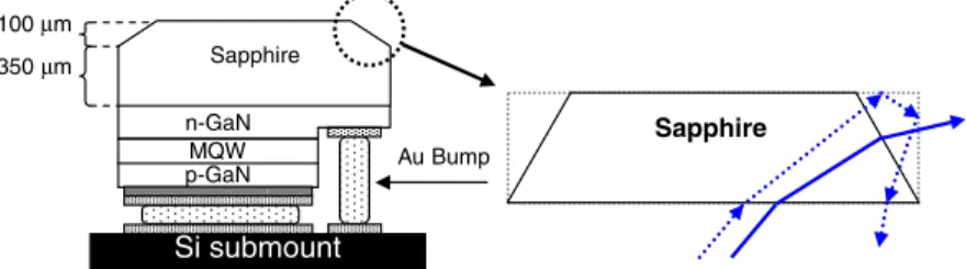
light-Semicond. Sci. Technol. 23 (2008) 025015 C E Lee et al Au Bump Sapphire Si submount n-GaN p-GaN MQW Sapphire 100 m 350 m
Figure 1. Schematic drawing of the GaN-based SSFC-LEDs, illustrating the means by which light may be extracted from the oblique
sapphire sidewall.
output enhancement in a nitride-based light-emitting diode with 22◦ undercut sidewalls [8]. All these methods have one thing in common, which is that photons generated within the LEDs can experience multiple opportunities to find the escape cone. As a result, the light extraction efficiency and the LED output intensity could both be enhanced significantly. It is said that a simple method to fabricate oblique sidewall will be beneficial to raise the brightness of the nitride-based LEDs. In this work, the nitride-based FC-LEDs with a geometric sapphire shaping structure were developed. The formation of oblique sapphire sidewalls on the bottom side of the sapphire surface can be a better way to improve the probability of photons escaping through the oblique sidewalls. The electrical and optical properties of the sapphire-shaped FC-LEDs (SSFC-LEDs) are reported.
Device fabrication
The GaN LED structure with dominant wavelength at 460 nm used in this study was grown by metal–organic chemical vapor deposition (MOCVD) on C-plane sapphire substrates. The LED structure consists of a 2 µm thick undoped GaN layer, a 2 µm thick highly conductive n-type GaN layer, a 0.2 µm thick InGaN/GaN MQW, a 0.2 µm thick p-type GaN layer and n InGaN/GaN short period super-lattice (SPS) tunneling contact layers for indium-tin-oxide (ITO). First, the SiO2film with a
size of 1000 µm× 1000 µm was deposited onto the backside of the sapphire substrate by plasma-enhanced chemical vapor deposition and defined using standard photolithography to serve as the wet etching hard mask. In order to prevent the damage of front epi-layer during the high temperature sapphire wet etching, the front epi side was covered by a 3 µm thick SiO2film for the passivation purpose. The sapphire substrate
was then immersed into a H2SO4:H3PO4(3:1) solution at an
etching temperature of 330 ◦C for 70 min. The sapphire wet etching rate is about 1.4 µm min−1 in this study and can be related to the H3PO4 composition and the etching
temperature. After finishing the sapphire shaping process, top-emitting LEDs with a size of 1000 µm× 1000 µm were fabricated using the standard photolithography process, which were aligned with the backside sapphire shaping pattern and were partially etched using an inductively coupled plasma etcher to expose an n-GaN layer for electrode formation. An ITO film (250 nm) was deposited on the p-GaN layer as the transparent conductive layer by an e-beam evaporator. The samples were then annealed at 500◦C for 10 min in air. The Cr/Pt/Au (50 nm/50 nm/2500 nm) metals were deposited for
(a) (b) Sapphire Etching time C-plane R-plane Oblique angle~60° (c)
Figure 2. Scanning electron micrographs of sapphire shaping
structure (a) cross-section and (b) top views. (c) Formation of the V-shape groove with etching time.
the p- and n-contact pads. After conventional LED processes, the processed LED wafer was subjected to the laser scribed and broken into 1000× 1000 µm2chips. Finally, the LED
chips with an oblique sapphire shaping sidewall were flip chip bonded on silicon sub-mount using the Panasonic ultrasonic flip-chip bonder for electrical and optical measurements. A schematic cross-sectional view of the GaN-based SSFC-LEDs with the oblique sapphire sidewall structure, illustrating the
(a) (b)
Figure 3. Scanning electron micrographs of (a) CFC-LED and (b) SSFC-LED devices.
(a) (b)
Figure 4. Photomicrographs of (a) CFC-LED and (b) SSFC-LED chips (40× 40 mil) operating at 20 mA (dc) with an emission wavelength
of λp∼460 nm.
means by which light may be extracted from the oblique sapphire sidewalls is shown in figure1.
Results and discussion
Figure 2 shows the scanning electron micrograph (SEM) images of sapphire shaping structure (a) cross-section and (b) top views. The oblique sidewall with a 100 µm etching depth could be obviously observed. The crystallography facets were (1 1 0 2) R-plane, (1 0 1 0) M-plane and (1 1 2 0) A-plane against the (0 0 0 1) c-axis and their angles against the (0 0 0 1) c-axis are about 60◦, 50◦ and 29◦, respectively. In this study, the sapphire was etched for 70 min via the etching rate of about 1.4 µm min−1and the etching depth was about 100 µm. Furthermore, the etching structures are all V-grooves. Figure 2(c) is a sample schematic illustration of the phenomenon mentioned above. According to this figure, the total area of (0 0 0 1) C-plane decreases as the etching time increases due to its relatively fast etching rate. On the other hand, the oblique surface of the (1 1 0 2) crystallography-etched facet increases with the etching time resulting in the formation of a V-shape groove. The V-shape structure can be used to form a cleaving line to break the thick (∼450 µm) sapphire substrate. The SEM images of SSFC-LED and conventional FC-LED devices are shown in figures 3(a) and (b). The sapphire shaping area and the thick windows layer were obviously observed on the SSFC-LED structure compared with the conventional FC-SSFC-LED. The oblique sapphire geometry improves light extraction by reducing totally internally reflected (TIR) photons from the sidewall interfaces, allowing them to escape through the oblique sidewall. In addition, the use of highly reflective
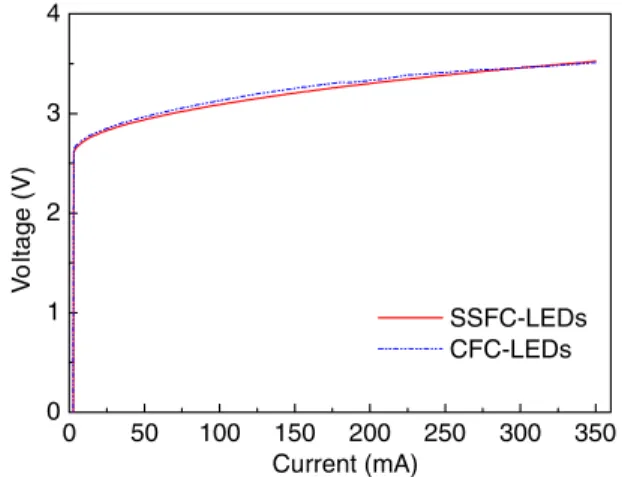
0 50 100 150 200 250 300 350 0 1 2 3 4 V o lt age ( V ) Current (mA) SSFC-LEDs CFC-LEDs
Figure 5. The corresponding current–voltage (I–V) characteristics
of CFC-LEDs and SSFC-LEDs.
omni-directional reflectors allows radiated light with any incident angle to be reflected to the top surface of the device, facilitating light emission from the oblique sidewalls. These two processes provide the SSFC-LED device with a significant reduction in the photon path length for extraction compared to a conventional chip. Such benefits are shown in the photomicrographs, figures4(a) CFC-LED and (b) SSFC-LED. Note that light appears to radiate evenly from the thicker windows layer and the oblique sidewall of the SSFC-LED (b) as compared with that of the CFC-LED (a), indicative of light extraction improvement via oblique sapphire geometry and ODR. The corresponding I–V characteristics of SSFC-LEDs and CFC-SSFC-LEDs were also measured, respectively, as shown in figure 5. It was found that the I–V curve of
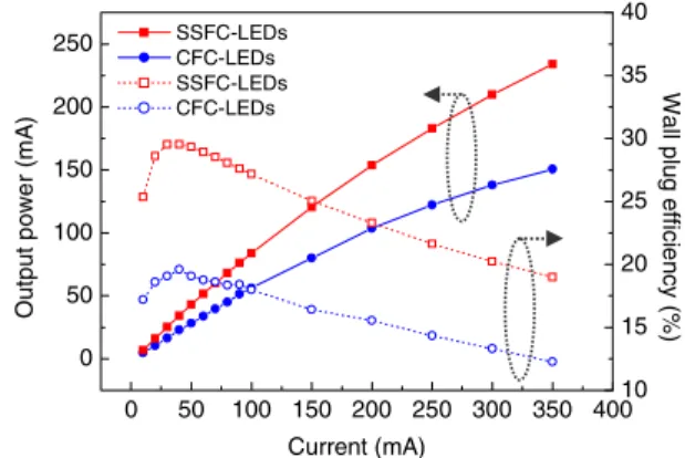
Semicond. Sci. Technol. 23 (2008) 025015 C E Lee et al 0 50 100 150 200 250 300 350 400 0 50 100 150 200 250 SSFC-LEDs CFC-LEDs SSFC-LEDs CFC-LEDs Current (mA) Out p ut p o we r (m A ) 10 15 20 25 30 35 40 W a ll pl ug eff ici e n cy (% )
Figure 6. The light output power and wall plug efficiency as a
function of injection current for λp∼ 460 nm devices of CFC-LEDs
and SSFC-LEDs.
SSFC-LEDs exhibits a normal p–n diode behavior with a forward voltage (at 350 mA) of 3.5 V, indicating that the high
(a) (b)
Figure 7. The 3D far-field patterns of (a) CFC-LED and (b) SSFC-LED. (Colour online.)
sapphire n-GaN p-GaN (a) sapphire n-GaN p-GaN Etching depth (b)
Figure 8. The simulated candela maps and ray-tracing images of (a) CFC-LEDs and (b) SSFC-LEDs, respectively. (Colour online.) temperature sapphire wet etching process does not appear to adversely affect I–V characteristics of these devices. Figure6
shows the light output power and wall plug efficiency as a function of injection current for λp ∼ 460 nm devices
of CFC-LEDs and SSFC-LEDs. It is clearly observed that the light output powers of the SSFC-LEDs were larger than those of the CFC-LEDs. Under 350 mA current injections, it is found that the enhancement of light output powers of the SSFC-LEDs and CFC-LEDs could be significantly raised from 150 mW to 234 mW and the wall plug efficiency could be increased from 12.26% to 18.98%. We note that bare SSFC-LEDs (without an epoxy lens encapsulated) exhibit 55% light extraction efficiency enhancement at 350 mA current injections compared to the CFC-LEDs. Such an enhancement could be ascribed to the geometric sapphire shaping structure and ODR, which reduces the totally internally reflected photons from the oblique sidewall interface and improves the probability of photons escaping from semiconductor to air. It is noted that the SSFC-LEDs offer a significant advantage
over CFC-LEDs by facilitating light emission from the oblique sidewalls of the chip. In order to verify the light extraction of the oblique sidewalls, a 3D far-field pattern of SSFC-LED and CFC-LED under 20 mA current injection, respectively, is shown in figure 7. It can be obviously observed that the SSFC-LEDs present a larger far-field pattern than that of CFC-LEDs in the near horizontal directions. Such an enhancement could be attributed to the oblique sidewall and thicker sapphire windows layer such that photons could have a higher probability to be emitted from the device in the near horizontal directions. The improved light extraction efficiency can be further supported by the simulation result using the ray-tracing method. Figures8(a) and (b) show the simulated candela maps and ray-tracing images of CFC-LEDs and SSFC-LEDs, respectively. The intensity of SSFC-LEDs obviously exceeds that of CFC-LEDs. The corresponding ray-tracing images of the oblique sidewall indicate that a large number of light rays can be extracted from the oblique sidewall due to the reduction of total internal reflection and the improvement in probability of photons escaping from semiconductor to air.
Conclusion
In summary, the FC-LEDs with geometric sapphire shaping structure and a thick sapphire windows layer were investigated. The formation of SSFC-LEDs structure increased the light output power up to 55%. The novel FC-LEDs structure could not only reduce the TIR effect, but also facilitate light emission from the edges of the thicker sapphire windows layer resulting in an increase in the light extraction efficiency of FC-LEDs.
From ray-tracing simulation results, the geometrical sapphire shape structure was confirmed to provide a greater probability of photons escaping from the sapphire/air interface, making an increase in the light extraction efficiency.
Acknowledgments
This work was supported by the MOE ATU program and in part by the National Science Council of Republic of China (ROC) in Taiwan under contract nos NSC 95-2120-M-009-008 and NSC 94-2215-E-009-082.
References
[1] Schubert E F and Kims J K 2005 Science308 1274–8
[2] Zukauskas A, Shur M S and Gaska R Introduction to Solid-State Lighting (New York: Wiley)
[3] Chang S J, Chang C S, Su Y K, Lee C T, Chen W S, Shen C F, Hsu Y P, Shei S C and Lo H M 2005 IEEE Trans. Adv. Packag.28 273–7
[4] Hibbard D L, Jung S P, Wang C, Ullery D, Zhao Y S, So W, Liu H and Lee H P 2003 Appl. Phys. Lett.83 311–3
[5] Krames M R et al 1999 Appl. Phys. Lett.75 2365–7
[6] Eisert D and Harle V 2002 Int. Conf. Numerical Simulation of Semiconductor Optoelectronic Devices, Session 3: Photonic Devices, invited paper
[7] Chang C S, Chang S J, Su Y K, Lee C T, Lin Y C, Lai W C, Shei S C, Ke J C and Lo H M 2004 IEEE Photon. Technol. Lett.16 750–2
[8] Kao C C, Kuo H C, Huang H W, Chu J T, Peng Y C, Hsieh Y L, Luo C Y, Wang S C, Yu C C and Lin C F 2005 IEEE Photon. Technol. Lett.17 19–21
[9] Kim J K, Gessmann T, Schubert E F, Xi J Q, Luo H, Cho J, Sone C and Park Y 2006 Appl. Phys Lett.88 013501