國 立 交 通 大 學
電 子 工 程 學 系 電 子 研 究 所
碩 士 論 文
超薄雙閘極金氧半場效電晶體與矽奈米線電晶體
涵蓋通道背向散射效應之物理解析模型
Channel Backscattering Based Analytic Model
for Double-Gate MOSFETs and Silicon Nanowire Transistors
研 究 生:顏士貴 Shih-Guei Yan 指導教授:陳明哲 Prof. Ming-Jer Chen
超薄雙閘極金氧半場效電晶體與矽奈米線電晶體
涵蓋通道背向散射效應之物理解析模型
Channel Backscattering Based Analytic Model
for Double-Gate MOSFETs and Silicon Nanowire Transistors
研 究 生:顏士貴 Student:Shih-Guei Yan
指導教授:陳明哲 Advisor:Prof. Ming-Jer Chen
國 立 交 通 大 學
電子工程學系 電子研究所碩士班
碩 士 論 文
A Thesis
Submitted to Department of Electronics Engineering & Institute of Electronics
College of Electrical Engineering and Computer Science National Chiao Tung University
in Partial Fulfillment of the Requirements for the Degree of
Master of Science In
Electronics Engineering July 2006
超薄雙閘極金氧半場效電晶體與矽奈米線電晶體
涵蓋通道背向散射效應之物理解析模型
研究生:顏士貴 指導教授:陳明哲博士
國立交通大學
電子工程學系電子研究所
摘 要
根據通道背向散射效應的基本理論,其物理解析式模型主要是建 立 在 源 極 到 通 道 的 能 障 頂 端 上 的 kBT layer 內 。 經 由 利 用 一 維 Schrödinger 和 Poisson 模擬,再透過不同結構模型的運算,可驗證此 模型之正確性;或者利用Monte Carlo 原理去模擬在不同條件下之電 子束反射與透射的關係,亦可做為檢驗此模型之依據。此論文將分別 針對超薄雙閘極金氧半場效電晶體和矽奈米線電晶體的模型來做模 擬分析與比較,並且得出合理的結果。Channel Backscattering Based Analytic Model for
Double-Gate MOSFETs and Silicon Nanowire Transistors
Student:Shih-Guei Yan Advisor:Prof. Ming-Jer Chen
Department of Electronics Engineering Institute of Electronics
National Chiao Tung University
Abstract
According to the fundamental theory of the channel backscattering, a physically based analytic model is established in the kBT layer at the peak
of the source-channel barrier. By using the 1-D Schrödinger-Poisson simulation and the evaluations of the underlying different structures, the validity of the model can be corroborated. Simulation for the forward and backward flux relation under different conditions by the Monte Carlo technique can also confirm the validity of the model. In this thesis, a series of physically-based analytic models applied to ultra-thin double-gate MOSFETs and silicon nanowire transistors are analyzed and testified. The reasonable results are achieved.
致 謝
轉眼間碩士班兩年的時光就這樣過去了,時間雖然短暫,但是卻讓我體驗到 了前所未有的充實感,了解到許多所謂的專業,也學到了許多做研究的精神和解 決問題的態度與方法,最後終於完成這份論文,這其中要感謝的人還真不少。 首先,第一個要感謝的當然是陳明哲教授,在這兩年的耳濡目染之下,充分 地感受與學習到老師對物理的嚴謹態度,再加上老師的指導與信任,讓我得以放 心地做研究,並且一步一步地順利完成每一個階段的任務。在此我要由衷地向老 師表達我的感謝之意。 其次要感謝的,就是實驗室的夥伴們。呂明霈學長提供給我在很多事情上的 經驗與意見,無論是專業或者日常生活,都讓我得以避免很多不必要的錯誤;謝 振宇學長與我的專業討論,讓我省掉很多自行摸索的時間;李建志充分發揮了戰 友情誼,在自己忙碌之餘,亦時常主動關心,希望能提供幫助;蔡鐘賢與曾貴鴻 也扮演了稱職的戰友角色,沒有他們和我一起常常待到晚上十一點,我一個人恐 怕很難發揮強大的鬥志;學弟許智育與李韋漢在專業上也都提供了夠份量的幫 助,也帶給實驗室不少歡樂。 最後要感謝的是幕後英雄,其中最重要的是我的哥哥顏碩廷博士,以親人兼 學長的身分給了我許多直接的幫助;我的父母、妹妹,還有許許多多的親朋好友 給予我的經常性關心,都是我一路走來很強大的支柱。 我想這幾段話是沒辦法一一謝過所有關心我的人的,故謹以此微不足道之感 言獻給每一位關心我的人,感謝你們,謝謝! 顏士貴 誌于風城交大 2006Contents
Abstract (Chinese) ...i
Abstract (English) ...ii
Acknowledgement ...iii
Contents ...iv
List of Captions...vi
Chapter 1 Introduction
...1Chapter 2 Physically Based Analytic Model for 2-D Devices
..42.1 Device Under Study...4
2.2 Model Establishment ...4
2.3 Analysis with 2-D model ...7
2.4 Results...8
Chapter 3 Low-Field Mobility of Electrons in Bulk Silicon
...103.1 Channel Backscattering Coefficient ...10
3.2 Electron Transport Simulation...10
3.3 Low-Field Mobility of Electrons ...12
Chapter 4 Physically Based Analytic Model for 1-D case
...134.2 Model Establishment ...13
4.3 Analysis with 1-D model ...16
4.4 Results...16
Chapter 5 Conclusion
...17List of Captions
Fig. 1-1 Schematic diagram of channel backscattering theory. F is the incident flux from the source, l is the critical length over which
a kBT/q drop is developed, and rC is the channel backscattering
coefficient. The channel length Leff is the physical gate length
minus the source/drain extensions...21 Fig. 2-1 Schematic cross section of the device under study...22
Fig. 2-2 Schematic conduction-band profile from source to drain. An E-k diagram is plotted showing forward and backward flux at the peak of the source-channel barrier ...23
Fig. 2-3 Channel subband levels and Fermi level versus gate voltage obtained from 1-D self-consistent Schrödinger-Poisson simulation ...24
Fig. 2-4 Channel subband level occupancy versus gate voltage from 1-D self-consistent Schrödinger-Poisson simulation ...25
Fig. 2-5 Flowchart of our analysis...26
Fig. 2-6 kBT layer width versus XR-Scatt quoted from [9] for L=25nm. The
Fig. 2-7 Schematic flux profile in the kBT layer when the factor Q’ is
considered...28
Fig. 2-8 In order to analyze, we must transform the flux profile to adapt our model...29
Fig. 2-9 Comparison of calculated drain current versus XR-Scatt with that
from Monte Carlo particle simulation...30
Fig. 2-10 Comparison of calculated barrier height versus XR-Scatt with that
from Monte Carlo particle simulation...31
Fig. 2-11 Comparison of calculated drain current versus XR-Scatt with that
from Monte Carlo particle simulation...32
Fig. 3-1 Schematic structure of the simulation in the model “channel”...33
Fig. 3-2 An example case of the schematic velocity distribution. The backscattering coefficient rC is just equal to the area ratio of
negative to positive...34
Fig. 3-3 The simulated backscattering coefficient of Monte Carlo evaluation under electric field from 10 V/cm to 106 V/cm for L = 80 nm and L = 20 nm ...35
Fig. 3-4 The mean-free-path λ extracted from the rC-E relation ...36
Fig. 3-5 The low-field mobility of electrons ...37
Fig. 4-1 (a) A schematic diagram of the simulated nanowire FETs. (b) Schematic cross section of the Si nanowire under study...38
Fig. 4-2 The density-of-state effective mass at Γ point in the wire conduction band versus wire diameter D for a [100] oriented Si nanowire ...39
Fig. 4-3 Comparison of calculated drain current by (a) linear and (b) logarithmic scale versus VGS with that from Büttiker probes
model. Here we assumed that rC is consistent in a whole range
Chapter 1
Introduction
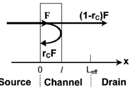
As the feature lengths of metal-oxide-semiconductor field effect transistors (MOSFETs) continue to scale into the nanoscale regime, short channel effects become more and more significant and quantum mechanics is expected to govern the underlying transport details. Consequently, an effective gate control is required for a nanoscale MOSFET to achieve good device performance. Therefore, some advanced MOSFET structures such as double-gate MOSFETs or silicon nanowire transistors (SNWTs) have been proposed and explored in the past years to exhibit their good gate controllability. It is generally recognized that while carriers, during the operation of the device, encounter significant space confinements and few scatterings, the conventional semiconductor transport theory would lose its accuracy in addressing such situations. In order to deal with this issue, channel backscattering theory has recently been introduced to provide the mesoscopic aspects of carrier transport in nanoscale MOSFETs [1]-[7].
The channel backscattering theory describes a wave-like transport of carriers through the channel from source to drain. In the schematic illustration of the theory for the saturation case shown in Figure 1-1, a kBT
layer, where kB is Boltzmann’s constant and T is the temperature, represents
the region from the peak of the source-channel junction barrier down by a thermal energy of kBT, and its width is denoted by l [2]-[7]. This specific
zone located near the source critically determines the current drive at the drain
1 1 C D tot inj C r I Q v r − = + (1.1)
where Qtot is the total charge density per unit area at the top of the
source-channel junction barrier, vinj the thermal injection velocity at the top
of the source-channel junction barrier, and rC is the channel backscattering
coefficient through the layer. The term Qtot/(1+rC) is related to the carriers
injected from the source and (1-rC) is the ratio of carriers traveling across the
barrier to the drain. The theory also argues that the backscattering coefficient
rC is functionally linked to both the quasi-thermal-equilibrium
mean-free-path λ for backscattering and the width l of the kBT layer
1 1 C r l λ = + (1.2)
In this thesis, a 2-D physically-based analytic model established at the peak of the source-channel barrier for double-gate MOSFETs [8]-[11] and a 1-D model for silicon nanowire transistors [8], [11]-[14] with channel length down to 25nm and 10 nm, respectively, have been demonstrated. Additionally, an the 1-D Monte Carlo particle simulation [8] is utilized to explore the backscattering coefficient rC , and its mean-free-path λ is
straightforwardly extracted to investigate the low-field mobility of electrons in silicon [6].
This thesis is organized as follows. In Chapter 2, we exhibit the 2-D model for double-gate MOSFETs and compare it with Monte Carlo simulation results [9]. Subsequently, in Chapter 3, the low-field mobility of
electrons in silicon with Monte Carlo particle simulation is studied [6]. In Chapter 4, the 1-D model for the silicon nanowire transistors is demonstrated and compared with another model called Büttiker probes [12]. Finally, a conclusion of the work will be shown in Chapter 5.
Chapter 2
Physically Based Analytic Model for 2-D Devices
2.1 Device Under Study
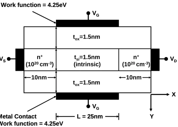
Figure 2-1 describes the cross section of the double-gate MOSFET structure under study: a 1.5-nm-thick silicon film double-gate MOSFETs with channel length equal to 25 nm. The gate length L is equal to the channel length. The top and bottom gate oxide thickness are tox=1.5 nm, and the Si
body thickness tSi is also 1.5 nm. The n+ source and drain are degenerately
doped at a level of 1020 /cm3, and the whole channel region is undoped. The
low-field mobility is assumed to be 120 cm2/V-sec, and the work function of the top and bottom gate is 4.25 eV. All the simulations are conducted at room temperature (T=300 K). To obtain the steady-state behavior of the device, the same voltage of 0.56V is applied to both the top gate and bottom gate, which results in the same work function with symmetry.
2.2 Model Establishment
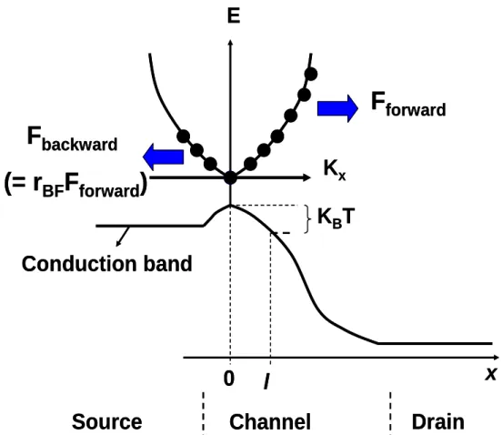
With the concepts of the elementary scattering theory, we established a 2-D model for the double-gate system. Figure 2-2 shows the conduction band profile from source to drain along with the electron energy versus wave vector plot at the peak of the barrier showing the ratio of backward to forward flux, rBF. The forward flux from the source side brings a carrier
density nS(+) and the backward flux is nS(-). Then the ratio rBF can be
BF S
( )
( )
Sn
r
n
−
=
+
(2.1)At the top of the source-channel junction barrier, the total carrier density nS
is nS =nS( )+ +nS( )− (2.2) and S Si i n =
∑
n (2.3) Here i Sn is the carrier density with subband i. It can be developed that
(
1)
2 2 ln 1 F i B E E i k T i d B i S BF v m k T n r n eπ
− ⎛ ⎞ ⎡ ⎤ = + ⎢ ⎥ ⎜⎜ + ⎟⎟ ⎣ h ⎦ ⎝ ⎠ (2.4) where i vn is the valley degeneracy and i d
m is the density-of-states
effective mass for subband i.
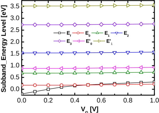
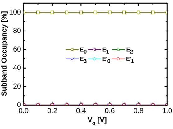
With the model for the above double-gate system, A self-consistent Schrödinger-Poisson simulation [8] was performed on a 1-D upper metal-gate oxide-silicon film-gate oxide-bottom metal system, yielding channel subband levels and Fermi level versus gate voltage as shown in Figure 2-3. According to the 1-D simulation results in Figure 2-4, almost all
of the electrons occupy the first subband of the two-fold valley (i.e. i v
n =2),
therefore the carrier density only on the first subband (i.e. i=1, n1S=nS) can
be reasonably calculated [3]. With the same subband and Fermi-level, the effective thermal injection velocity at the top of source-junction barrier is as follows: 2 1/ 2
( )
2 ln(1 F) i F i B C inj i d k Tm m eηη
υ
π
ℑ ⎛ ⎞ = ⎜ ⎟ + ⎝ ⎠ (2.5) 1/ 2 1/ 2 1/ 2 0 0 1 2 ( ) 3 1 1 2 F F F F i F B d d e e E E k T η η η η η η η η η π η ∞ ∞ − − ℑ = = + + ⎛ ⎞ Γ⎜ ⎟⎝ ⎠ − =∫
∫
where i Cm is the conductivity effective mass for subband i, Ei the energy
level of subband i, EF the Fermi-level, and ℑ1/ 2 is the Fermi-Dirac integral
of order 1/2. For two-fold valley, i C
m =mdi = mt , where the transverse
effective mass mt = 0.19m0 .
The mean-free-path λ for backscattering is exhibited as follows:
(
) (
)
1 ln 1 2 F F F B inj e e k T q e η η ηµ
λ
υ
+ + = (2.6)where μ is the quasi-equilibrium mobility. The backscattering coefficient
1 1 C r l
λ
= + (2.7)where l is the width of the kBT layer. The drain current can therefore be
obtained: DS S inj11 C C r I qn v r − = + (2.8)
2.3 Analysis with 2-D model
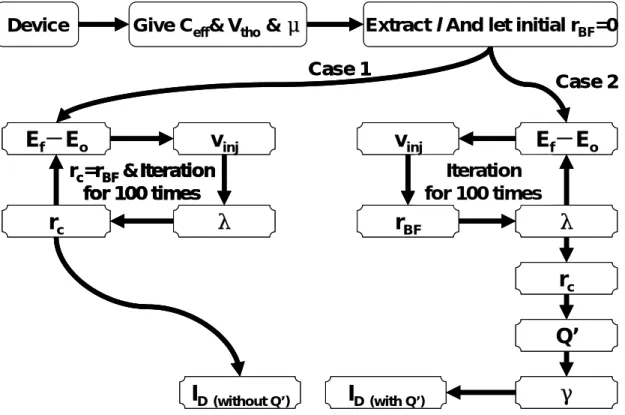
Figure 2-5 is the flow chart of our analysis. According to MOS electrostatics [3], we have
qnS =Ceff[VG −(Vtho−DIBL V× D)] (2.9)
The effective gate capacitance Ceff and qusi-equilibrium threshold voltage
Vtho can be assessed via the Schrödinger-Poisson solver under zero DIBL [8].
The kBT layer widths are extracted from the simulated potential profiles for
different scattering areas cited in [9] as shown in Figure 2-6.
In case 1, the carriers scattering only occurs in the kBT layer is
considered. Hence, the ratio of backward to forward flux rBF is equal to the
channel backscattering coefficient rC [5]. Through the iteration method with
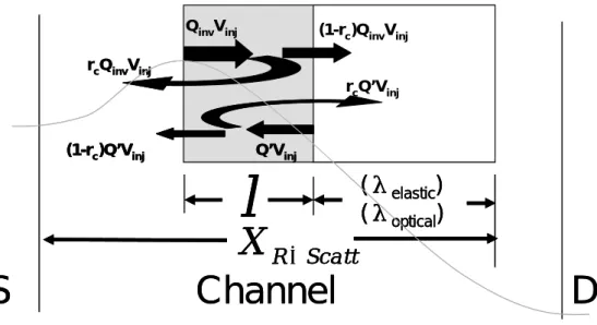
carriers pass through the kBT layer, additional elastic and inelastic scattering
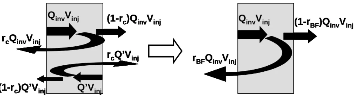
effect may occur [9].Consequently, the flux plot is shown in Figure 2-7. We have transformed the flux plot to apply to our model as shown in Figure 2-8, where the rBF can be shown as a function of rc:
BF C (1 C) ' inv Q r r r Q = + − (2.10)
The term Qinv is defined as the carriers injected from source and Q’ the
carriers reflected from the scattering zone after the carriers pass through the kBT layer. After iteration process, the coefficient of rBF is obtained with the
drain current of 1 1 BF DS S inj BF r I qn v r − = + (2.11)
Here the IDS is called ID(with Q’) to imply that the additional elastic and
inelastic scattering effects are considered.
2.4 Results
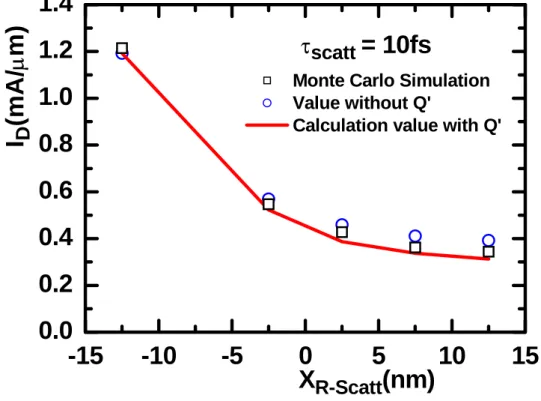
To examine the validity of the channel backscattering theory, we have compared the calculated results with those from 2-D Monte Carlo particle simulation [9]. The calculation values in case 2 are considerably consistent with the Monte Carlo particle simulation results as exhibited in Figure 2-9. Furthermore, corroborating evidence in terms of the height of the source-channel junction barrier is given in Figure 2-10. However, as the
mobility μ or scattering time τ is increased by a factor of 5, implying that the channel length is effectively reduced from 25nm down to 5nm, the calculated drain currents is also consistent with the Monte Carlo particle simulation results as shown in Figure 2-11. Consequently, the channel backscattering theory remains valid in this study.
Chapter 3
Low-Field Mobility of Electrons in Bulk Silicon
3.1 Channel Backscattering Coefficient
In this study, if the channel is under low electric field conditions, the width of the kBT layer l calculated according to its definition is wide enough
to be larger than the channel length L. Therefore, the backscattering coefficient can be estimated from
Co L r L λ = + (3.1)
where λ is the mean-free-path, L is the channel length which is smaller than the kBT layer width l, implying that the scattering effect is only
assumed to occur in channel. When a strong channel electric field is present, i.e. l < L, the backscattering coefficient can be accordingly estimated from
C l r l
λ
= + (3.2)3.2 Electron Transport Simulation
In order to explore the backscattering coefficient rC , we have
simulated electron transport through one-dimensional silicon devices by the Monte Carlo technique [8]. A model “channel” with length L = 80 nm or 20 nm is divided into 100 grids to analyze the forward and backward flux in
each grid, and a constant electric field is applied. Figure 3-1 shows the schematic structure of the simulation in the model “channel”. The doping concentration is set to be 8×10¹⁷ /cm3 and the temperature is 300 K. From the definition of backscattering coefficient, we have
( ) ( ) C flux n v r flux n v − − + + − = = + (3.3) 0 0 0 0 0 0 ( ) ( ) ( ) ( ) ( ) ( ) f v dv n n f v dv f v vdv f v dv v v f v vdv f v dv − −∞ ∞ + −∞ − −∞ ∞ + ∞ = =
∫
∫
∫
∫
∫
∫
where n± is the electron density for forward/backward direction, and v± is the average velocity for forward/backward direction. Fig. 3-2 shows an example case of the schematic velocity distribution. Here the backscattering coefficient rC is just equal to the area ratio of negative to positive. Figure 3-3
shows the simulated backscattering coefficient of Monte Carlo evaluation under electric field from 10 V/cm to 106 V/cm for L = 80 nm and L = 20 nm. It is obvious that the backscattering coefficient is nearly constant at low electric field as a linear region. In contrast to low electric field, the backscattering coefficient for the higher electric field is lower in the saturation region, which is close to the ballistic limit.
3.3 Low-Field Mobility of Electrons
From the channel backscattering theory, since the backscattering coefficient rC is functionally linked to both the quasi-thermal-equilibrium
mean-free-path λ for backscattering and the width l of the kBT layer, the
mean-free-path λ can be obtained by fitting method. With the Monte Carlo simulation at different temperatures, the mean-free-path λ is extracted as shown in Figure 3-4. The mean-free-path is physically increased with the decrease of the temperature. Furthermore, the low-field mobility of electrons is calculated as shown in Figure 3-5. As a result, it is considerably reasonable [6] to keep the channel backscattering theory remaining valid in this study.
Chapter 4
Physically Based Analytic Model for 1-D case
4.1 Device Under Study
Figure 4-1 describes the diagram of the Si nanowire transistor structure under study: a cylindrical SNWT with <100> oriented channel length equal to 10 nm. The gate length L is equal to the channel length. The silicon body thickness TSi is 3 nm, and the oxide thickness is 1 nm. The source/drain
doping concentration is 2×10²⁰ /cm3 and the channel region is undoped. The low-field mobility is assumed to be 200 cm2/V-sec, and the work function of
the gate all around is 4.05 eV. All the simulations are conducted at room temperature (T=300 K) with the same voltage of 0.4V applied to both the gate and the drain.
4.2 Model Establishment
Similar to Chapter 2 of this thesis, we have also established a 1-D model for the nanowire transistor system with the concepts of the elementary scattering theory [11].
For 1-D case, the density-of-states is exhibited as follows:
1 2 1 ( ) 2 d D C m D E E E π = − = (4.1)
nanowire. Under steady-state, non-equilibrium conditions,
dN E( ) 0
dt = (4.2)
and we can solve it for the steady-state number of electrons in the device. Consequently, the total number of electrons is obtained via integration over the energy in the device as
(1 ) 2 2 1 2( ) i i d B i s BF v F m k T n r n
η
π
− = + ℑ = (4.3) where i vn is the valley degeneracy, i d
m is the density-of-states effective
mass for subband i, and ℑ-1/ 2 is the Fermi-Dirac integral of order -1/2 as
shown below 1/ 2 1/ 2 1/ 2 0 0 1 1 ( ) 1 1 1 2 F F F d d eη η eη η η η η η η π − ∞ ∞ − − − ℑ = = + + ⎛ ⎞ Γ⎜ ⎟ ⎝ ⎠
∫
∫
(4.4) F F i B E E k T η = −where Ei is the energy level of subband i, and EF is the Fermi-level. In this
study, it is assumed that almost all of the electrons occupy the lowest subband (i.e. i=1, n1S =nS), which is the first subband of the four-fold valley
(i.e. i v
With the drain current contributed by subband, i, I 2qk TB ln(1 e F) h η ⎡ ⎤ = ⎣ + ⎦ (4.5) =qn vS inj
the effective thermal injection velocity at the top of source-junction barrier is as follows [4].
( )
1/ 2 2 ln(1 F) B inj i d F k T e m ηυ
π
−η
⎛ + ⎞ = ⎜⎜ ⎟⎟ ℑ ⎝ ⎠ (4.6)The mean-free-path λ for backscattering is exhibited as follows [10].
1 2 3 2 ( ) 2 ( ) F B inj F k T q
η
µ
λ
υ
η
− − ℑ = ℑ (4.7)where μ is the quasi-equilibrium mobility. The backscattering coefficient
rC is 1 1 C r l
λ
= + (4.8)1 1 C DS S inj C r I qn v r − = + (4.9)
4.3 Analysis with 1-D model
Similar to Chapter 2, by using the Schrödinger-Poisson solver, the effective gate capacitance Ceff and quasi-equilibrium threshold voltage Vtho
can be obtained with the relationship as follows:
qnS =Ceff(VG −Vtho) (4.10)
The kBT layer widths are extracted from the potential profiles of Fig. 3 in
[12]. The density-of-states effective mass is 0.28mo as shown in Figure 4-2
for wire diameter TSi equal to 3 nm [14]. Following the case 1 of the flow
chart in Chapter 2, the drain current at VG=VD=0.4V can be obtained.
4.4 Results
To examine the validity of the channel backscattering theory on 1-D case, we have compared the calculated results with those from another model called Büttiker probes [12]. The calculated drain currents appear to lie a little above the Büttiker probes ones as shown in Fig. 4-3. It suggests that the importance of the source-to-drain tunneling is increased for channel length down to below 10 nm. The existing channel backscattering formula might be improved with consideration of the source-to-drain tunneling effect.
Chapter 5
Conclusion
The physically based analytic models of the ultra-thin film double-gate MOSFETs and silicon nanowire transistors have been established. The validity of the models has been confirmed using sophisticated simulations such as 1-D Schrödinger-Poisson solving, 2-D and 1-D ballistic I-V simulations, and 1-D Monte Carlo particle simulations with the scattering in the channel. The issues of concern have been focused on the effect of backward to forward flux ratio on the thermal injection velocity at the top of the source-channel junction barrier. It is argued that the backward to forward flux ratio can determine the channel backscattering coefficient in the framework of the channel backscattering theory.
References
[1] S. Datta, Electronic Transport in Mesoscopic Systems. Cambridge, U.K.: Cambridge Univ. Press, 1995.
[2] M. S. Lundstrom, “Elementary scattering theory of the Si MOSFET,”
IEEE Electron Device Letters, vol. 18, pp. 361-363, July 1997.
[3] F. Assad, Z. Ren, S. Datta, and M. S. Lundstrom, “Performance limits of silicon MOSFET’s,” in IEDM Tech. Dig., Dec. 1999, pp. 547-550.
[4] F. Assad, Z. Ren, D. Vasileska, S. Datta, and M. S. Lundstrom, “On the performance limits for Si MOSFET’s: A theoretical study,” IEEE Trans.
Electron Devices, vol. 47, pp. 232-240, Jan. 2000.
[5] M. S. Lundstrom and Z. Ren, “Essential physics of carrier transport in nanoscale MOSFETs,” IEEE Trans. Electron Devices, vol. 49, pp. 133-141, Jan. 2002.
[6] Mark Lundstrom, Fundamentals of Carrier Transport, second edition, School of Electrical and Computer Engineering Purdue University, West Lafayette, Indiana, USA: Cambridge University Press, 2000.
[7] M. J. Chen, H. T. Huang, Y. C. Chou, R. T. Chen, Y. T. Tseng, P. N. Chen, and C. H. Diaz, “Separation of Channel Backscattering Coefficients in Nanoscale MOSFETs,” IEEE Trans. Electron Devices, vol. 51, pp. 1409-1415, September 2004.
[8] http://www.nanohub.org/
[9] A. Svizhenko and M. P. Anatram, “Role of scattering in nanotransistors,”
IEEE TED, p. 1459, 2003.
[10] A. Rahman and M. S. Lundstrom, “A compact scattering model for the nanoscale double-gate MOSFET,” IEEE TED, p. 481, 2002.
[11] M. S. Lundstrom, “Notes on Ballistic MOSFET,” Network for Computational Nanotechnology and Purdue University.
[12] J. Wang, E. Polizzi, M. S. Lundstrom, “A three-dimensional quantum simulation of silicon nanowire transistors with the effective-mass approximation,” Journal of Applied Physics, vol. 96, p. 2192, 2004.
[13] M. Bescond, N. Cavassilas, K. Kalna, K. Nehari, L. Raymond, J.L. Autran, M. Lannoo, A. Asenov, “Ballistic transport in Si, Ge, and GaAs nanowire MOSFETs,” in Proc. IEEE Int. Electron Devices Meeting, Dec. 5, 2005, pp. 526-529.
[14] Jing Wang, Anisur Rahman, Gerhard Klimeck and Mark Lundstrom, “Bandstructure and Orientation Effects in Ballistic Si and Ge Nanowire FETs” in Proc. IEEE Int. Electron Devices Meeting, Dec. 5, 2005, pp. 530-533.
Fig. 1-1 Schematic diagram of channel backscattering theory. F is the incident flux from the source, l is the critical length over which a
kBT/q drop is developed, and rC is the channel backscattering
coefficient. The channel length Leff is the physical gate length
L = 25nm n+ (1020 cm-3) n+ (1020 cm-3) tsi=1.5nm (intrinsic) tox=1.5nm tox=1.5nm 10nm 10nm VS VD VG VG Metal Contact
Work function = 4.25eV
Metal Contact
Work function = 4.25eV
Y X L = 25nm n+ (1020 cm-3) n+ (1020 cm-3) tsi=1.5nm (intrinsic) tox=1.5nm tox=1.5nm 10nm 10nm n+ (1020 cm-3) n+ (1020 cm-3) tsi=1.5nm (intrinsic) tox=1.5nm tox=1.5nm 10nm 10nm VS VD VG VG Metal Contact
Work function = 4.25eV
Metal Contact
Work function = 4.25eV
Y
X
Fig. 2-2 Schematic conduction-band profile from source to drain. An E-k diagram is plotted showing forward and backward flux at the peak of the source-channel barrier.
F
backward(= r
BFF
forward)
x
l
0
K
BT
Conduction band
F
forwardK
xE
Source
Channel
Drain
F
backward(= r
BFF
forward)
x
l
0
K
BT
Conduction band
F
forwardK
xE
0.0
0.2
0.4
0.6
0.8
1.0
0.0
0.5
1.0
1.5
2.0
2.5
3.0
3.5
Subba
nd_
Energy Le
ve
l [
e
V
]
V
G[V]
E f E0 E1 E2 E3 E'0 E'1Fig. 2-3 Channel subband levels and Fermi level versus gate voltage obtained from 1-D self-consistent Schrödinger-Poisson simulation.
0.0
0.2
0.4
0.6
0.8
1.0
0
20
40
60
80
100
Subband O
c
cupancy [%]
V
G[V]
E0 E1 E2 E3 E'0 E'1Fig. 2-4 Channel subband level occupancy versus gate voltage from 1-D self-consistent Schrödinger-Poisson simulation.
Extract l And let initial rBF=0 rc=rBF & Iteration for 100 times ID (without Q’) rc λ vinj Ef-Eo
Device Give Ceff& Vtho& μ
Iteration for 100 times vinj λ rc rBF Ef-Eo Q’ γ ID (with Q’) Case 1 Case 2 Extract l And let initial rBF=0
rc=rBF & Iteration for 100 times ID (without Q’) rc λ vinj Ef-Eo rc=rBF & Iteration for 100 times ID (without Q’) rc λ vinj Ef-Eo
Device Give Ceff& Vtho& μ
Iteration for 100 times vinj λ rc rBF Ef-Eo Q’ γ ID (with Q’) Iteration for 100 times vinj λ rc rBF Ef-Eo Q’ γ ID (with Q’) Case 1 Case 2
X
R-Scatt(nm)
k
BT
lay
er
w
id
th
l
(nm
)
τscatt= 10 fs
Source Scattering Drain
Region 0 XR-Scatt X Non-Scattering Region -15 -10 -5 0 5 10 15 2 4 6 8 1 0 1 2 14
X
R-Scatt(nm)
k
BT
lay
er
w
id
th
l
(nm
)
τscatt= 10 fs
Source Scattering Drain
Region 0 XR-Scatt X Non-Scattering Region
X
R-Scatt(nm)
k
BT
lay
er
w
id
th
l
(nm
)
τscatt= 10 fs
Source Scattering Drain
Region
0 XR-Scatt X
Non-Scattering Region
Source Scattering Drain
Region 0 XR-Scatt X Non-Scattering Region -15 -10 -5 0 5 10 15 2 4 6 8 1 0 1 2 14
Fig. 2-6 kBT layer width versus XR-Scatt quoted from [9] for L=25nm. The
(λelastic) (λoptical) R S c a tt
X
− rcQ’Vinj (1-rc)Q’Vinj Q’VinjD
rcQinvVinj QinvVinj (1-r c)QinvVinjS
Channel
l
(λelastic) (λoptical) R S c a ttX
− rcQ’Vinj (1-rc)Q’Vinj Q’Vinj (λelastic) (λoptical) R S c a ttX
− rcQ’Vinj (1-rc)Q’Vinj Q’VinjD
rcQinvVinj QinvVinj (1-r c)QinvVinjS
Channel
l
Fig. 2-7 Schematic flux profile in the kBT layer when the factor Q’ is
rBFQinvVinj QinvVinj (1-r BF)QinvVinj (1-rc)QinvVinj rcQinvVinj QinvVinj (1-rc)Q’Vinj rcQ’Vinj Q’Vinj rBFQinvVinj QinvVinj (1-r BF)QinvVinj rBFQinvVinj QinvVinj (1-r BF)QinvVinj (1-rc)QinvVinj rcQinvVinj QinvVinj (1-rc)Q’Vinj rcQ’Vinj Q’Vinj (1-rc)QinvVinj rcQinvVinj QinvVinj (1-rc)Q’Vinj rcQ’Vinj Q’Vinj rcQinvVinj QinvVinj (1-rc)Q’Vinj rcQ’Vinj Q’Vinj
Fig. 2-8 In order to analyze, we must transform the flux profile to adapt our model.
-15
-10
-5
0
5
10
15
0.0
0.2
0.4
0.6
0.8
1.0
1.2
1.4
Monte Carlo Simulation Value without Q'
Calculation value with Q'
τ
scatt= 10fs
I
D(mA/
µ
m)
X
R-Scatt(nm)
Fig. 2-9 Comparison of calculated drain current versus XR-Scatt with that from
-15
-10
-5
0
5
10
15
0
20
40
60
80
100
Monte Carlo simulation Calculation value with Q'
τ
scatt= 10fs
Barrier Hei
g
h
t (meV)
X
R-Scatt(nm)
Fig. 2-10 Comparison of calculated barrier height versus XR-Scatt with that
-15
-10
-5
0
5
10
15
0.0
0.2
0.4
0.6
0.8
1.0
1.2
1.4
Monte Carlo Simulation Value without Q'
Calculation value with Q'
τ
scatt= 50fs
I
D(mA/
µ
m)
X
R-Scatt(nm)
Fig. 2-11 Comparison of calculated drain current versus XR-Scatt with that
Source Drain Incident Beam L : Channel Length l : kBT Layer Source Drain Incident Beam L : Channel Length l : kBT Layer
-5.00x10⁷ -2.50x10⁷ 0.00 2.50x10⁷ 5.00x10⁷ 0.0 0.2 0.4 0.6 0.8 1.0
Distribution Function
velocity(cm/s)
Fig. 3-2 An example case of the schematic velocity distribution. The backscattering coefficient rC is just equal to the area ratio of
10
110
210
310
410
510
60.0
0.2
0.4
0.6
0.8
rc
Electric Field (V/cm)
L=80nm
L=20nm
Fig. 3-3 The simulated backscattering coefficient of Monte Carlo evaluation under electric field from 10 V/cm to 106 V/cm for L = 80 nm and L = 20 nm.
100 101 102 103 104 105 106 0.0 0.2 0.4 0.6 0.8 Maxwell Distribution L=80nm Nd=8x10¹⁷/cm3 3-D λ350=23.51nm λ300=24.07nm λ200=24.43nm λ77=24.88nm λ34=24.98nm λ24=24.99nm λ14=25nm
rc
Electric Field (V/cm) 350K 300K 200K 77K 34K 24K 14K+ λ
l
l
+ λ
L
L
100 101 102 103 104 105 106 0.0 0.2 0.4 0.6 0.8 Maxwell Distribution L=80nm Nd=8x10¹⁷/cm3 3-D λ350=23.51nm λ300=24.07nm λ200=24.43nm λ77=24.88nm λ34=24.98nm λ24=24.99nm λ14=25nmrc
Electric Field (V/cm) 350K 300K 200K 77K 34K 24K 14K 100 101 102 103 104 105 106 0.0 0.2 0.4 0.6 0.8 Maxwell Distribution L=80nm Nd=8x10¹⁷/cm3 3-D λ350=23.51nm λ300=24.07nm λ200=24.43nm λ77=24.88nm λ34=24.98nm λ24=24.99nm λ14=25nmrc
Electric Field (V/cm) 350K 300K 200K 77K 34K 24K 14K+ λ
l
l
+ λ
L
L
100 101 102 103 400 600 800 1000 1200 1400 1600 1800 2000 2200 2400 Maxwell Distribution L=80nm Mobili ty (cm 2 /V *s) Temprature (K) −
µ ∝
0.51T
* * * ce t l 1 1 2 1 m 3 m m ⎡ ⎤ = ⎢ + ⎥ ⎣ ⎦ * ce 0 m =0.267m = π * 2 / T B ce v k T m λ µ = * 2( ) T B v k T q 100 101 102 103 400 600 800 1000 1200 1400 1600 1800 2000 2200 2400 Maxwell Distribution L=80nm Mobili ty (cm 2 /V *s) Temprature (K) −µ ∝
0.51T
* * * ce t l 1 1 2 1 m 3 m m ⎡ ⎤ = ⎢ + ⎥ ⎣ ⎦ * ce 0 m =0.267m = π * 2 / T B ce v k T m λ µ = * 2( ) T B v k T qFig. 3-5 The low-field mobility of electrons
(a) (2x10²⁰/cm3) (undoped) (2x10²⁰/cm3)
V
GV
DV
SNanowire
Channel
Source
Exten.
Drain
Exten.
Gate All
Around
L
(2x10²⁰/cm3) (undoped) (2x10²⁰/cm3) (2x10²⁰/cm3) (undoped) (2x10²⁰/cm3)V
GV
DV
SNanowire
Channel
Source
Exten.
Drain
Exten.
Gate All
Around
L
L
(b)Fig. 4-1 (a) A schematic diagram of the simulated nanowire FETs. (b) Schematic cross section of the Si nanowire under study.
1
2
3
4
5
0.2
0.3
0.4
0.5
0.6
Diameter (nm)
m
dat
Γpoint (in m
o)
Fig. 4-2 The density-of-states effective mass at Γ point in the wire conduction band versus wire diameter D for a [100] oriented Si nanowire.
(a) (b) 0.0 0.1 0.2 0.3 0.4 0.0 3.0x10⁻⁶ 6.0x10⁻⁶ 9.0x10⁻⁶ 1.2x10⁻⁵ 1.5x10⁻⁵ 1.8x10⁻⁵ I D(ball.) ID(scatt.)(calculation) ID(scatt.)(Buttiker probes) IDS (A) VGS (V) 0.0 0.1 0.2 0.3 0.4 10-7 10-6 10-5 10-4 I D(ball.) I D(scatt.)(calculation) I D(scatt.)(Buttiker probes) IDS (A ) V GS (V)
Fig. 4-3 Comparison of calculated drain current by (a) linear and (b) logarithmic scale versus VGS with that from Büttiker probes model.
![Fig. 2-6 k B T layer width versus X R-Scatt quoted from [9] for L=25nm. The inset shows the definition of X R-Scatt](https://thumb-ap.123doks.com/thumbv2/9libinfo/8736991.203414/37.892.194.688.427.782/layer-width-versus-scatt-quoted-shows-definition-scatt.webp)