國 立 交 通 大 學
電子工程學系電子研究所碩士班
碩 士 論 文
鎵摻雜尖狀氧化鋅奈米柱陣列的場發射
與光學特性之研究
Field Emission and Optical Properties of Sharp
Ga-doped ZnO Nanorod Array
研 究 生:黃聖和
指導教授:曾俊元 教授
國 立 交 通 大 學
電子工程學系電子研究所碩士班
碩 士 論 文
鎵摻雜尖狀氧化鋅奈米柱陣列的場發射
與光學特性之研究
Field Emission and Optical Properties of Sharp
Ga-doped ZnO Nanorod Array
研 究 生:黃聖和
指導教授:曾俊元 教授
鎵摻雜尖狀氧化鋅奈米柱陣列的場發射
與光學特性之研究
Field Emission and Optical Properties
of Sharp Ga-doped ZnO Nanorod Array
研 究 生:黃聖和
Student : Sheng-He, Huang
指導教授:曾俊元
Advisor : Tseung-Yuen Tseng
國立交通大學
電子工程學系電子研究所碩士班
碩士論文
A Thesis
Submitted to Department of Electronics Engineering &
Institute of Electronics
College of Electrical and Computer Engineering
National Chiao Tung University
In Partial Fulfillment of the Requirements
for the Degree of Master
in Electronic Engineering
July 2011
Hsinchu, Taiwan, Republic of China
I
鎵摻雜尖狀氧化鋅奈米柱陣列的場發射
與光學特性之探討
研究生:黃聖和 指導教授:曾俊元 教授 國立交通大學 電子工程學系電子研究所碩士班摘要
近年來,奈米結構材料應用於場發射顯示器的發射源已被廣泛地 研究,其中以低溫製備的氧化鋅奈米柱最受到矚目。然而純的氧化鋅 奈米柱本身形貌不足以應用於場發射顯示器上。因此在本論文中,我 們藉由電漿蝕刻和摻雜方式去改善氧化鋅奈米柱的場發射特性。電漿 蝕刻是利用氧氣離子去轟擊奈米柱。摻雜製程是利用水熱法將鎵離子 摻雜進入奈米柱。最後,結合氧氣電漿蝕刻和摻雜鎵製程去形成尖狀 的鎵摻雜氧化鋅奈米柱。由量測結果可知,尖狀的鎵摻雜氧化鋅奈米 柱具有最佳的場發射特性與穩定性。此外,我們可以修補氧化鋅奈米 柱的表面缺陷,如此降低其可見光強度。II
Field Emission and Optical Properties
of Sharp Ga-doped ZnO Nanorod Array
Student : Sheng-He Huang Advisor : Tseung-Yuen Tseng
Department of Electronics Engineering & Institute of Electronics National Chiao Tung University
ABSTRACT
In recent years, nanostructures applied to serve as emitters of field emission display have been widely researched. ZnO nanorod arrays synthesized by hydrothermal method have been attracted much attention due to low temperature process. However, as-grown ZnO nanorod arrays cannot be applied to field emission display due to their morphologies. To improve field emission properties, we use plasma-treated process and doping process to fabricate ZnO nanorod arrays in this thesis. For plasma-treated process, we used oxygen ions to bombard nanorods. For doping process, we doped gallium ions by hydrothermal method. Finally, sharp Ga-doped nanorod arrays were fabricated by the combination of plasma-treated process and doping process. From our results, sharp Ga-doped nanorod arrays exhibit the best field emission properties and stabilities. In addition, we can repair the defects on the ZnO nanorod surfaces, so that it can reduce the intensity of visible emission.
III
致謝
首先,誠摯的感謝指導老師曾俊元教授悉心的教導,並提供如此資源 豐富的環境,並在專業領域上給予我許多的建議與方向,使我得以一窺固 態電子領域的深奧,順地完成本篇論文。此外,本篇論文的完成要特別感 謝奕全學長的熱心幫忙與建議,因為有你的意見與分析,使得實驗過程與 這篇論文得以更加的順利與完整。另外,感謝口試委員林鵬教授與田禮嘉 教授對於口試與論文內容,提供寶貴的意見與建議,使得本論文更加的完 善。 兩年的日子裡,有許多研究室裡共同的實驗生活以及課業上的檢討, 讓我特別珍惜這段的回憶。感謝聖裕、孟漢、明錡、崇榮、岱螢、駿揚、 佳宏、政漢、泰源、以煒和婉孜等學長學姐的指導與費心,宗翰、家瑋和 我共同努力及成長,以及宗霖和乙軒學弟們的陪伴,讓我這兩年的研究生 活變得絢麗多彩,謝謝實驗室的大家! 最後要感謝我的父母、妹妹以及外婆,很感激你們竭盡全力的支持我 讀研究所,讓我無後顧之憂順利的完成研究所學業,在此,將這份論文獻 給你們,這份喜悅是屬於你們的。IV
Contents
CHINESE ABSTRACT... I ENGLISH ABSTRACT ... II ACKNOWLEDGEMENT ... III CONTENTS ... IV TABLE CAPTIONS ... VII FIGURE CAPTIONS ... VIIICHAPTER 1 INTRODUCTION ... 1
1.1 Basic Properties of Zinc Oxide ... 1
1.2 Field Emission Display ... 2
1.3 Synthesis of Zinc Oxide Nanorods ... 4
1.4 Field Emission Principle... 7
1.5 Optical Properties of Zinc Oxide ... 9
1.6 Sharp Zinc Oxide Nanorods ... 11
1.7 Doped Zinc Oxide Nanorods ... 12
CHAPTER 2 EXPERIMENTAL DETAILS ... 20
2.1 Sample Preparation.. ... 20
2.1.1 Cleaning Wafer ... 20
V
2.1.3 Growth of ZnO Nanorod Array ... 21
2.1.4 Growth of Ga-doped Nanorod Array ... 21
2.1.5 Fabrication of Sharp Nanorods ... 21
2.2 Measurement and Analysis ... 22
2.2.1 Scanning Electron Microscopy (SEM) ... 22
2.2.2 Transmission Electron Microscopy (TEM) ... 22
2.2.3 X-ray Diffraction (XRD) ... 23
2.2.4 Photoluminescence (PL) ... 24
2.2.5 Field Emission Measurement ... 25
CHAPTER 3 RESULTS AND DISCUSSION ... 29
3.1 ZnO Seeding Layer ... 29
3.1.1 The SEM Analysis of Seeding Layer... 29
3.1.2 The XRD Analysis of Structure... 29
3.2 Ga-doped ZnO Nanorod Array ... 30
3.2.1 The SEM Analysis of Morphology ... 30
3.2.2 The XRD Analysis of Structure... 31
3.2.3 The TEM Analysis of Structure ... 31
3.2.4 The PL Spectrum of Structure ... 32
3.2.5 The Field Emission Measurement ... 32
3.2.6 The Stability of Field Emission Measurement ... 33
3.3 Sharp ZnO Nanorod Array ... 34
3.3.1 The SEM Analysis of Morphology ... 35
3.3.2 The XRD Analysis of Structure... 36
3.3.3 The TEM Analysis of Structure ... 36
VI
3.3.5 The Field Emission Measurement ... 38
3.3.6 The Stability of Field Emission Measurement ... 39
3.4 Sharp Ga-doped ZnO Nanorod Array ... 39
3.4.1 The SEM Analysis of Morphology ... 40
3.4.2 The PL Spectrum of Structure ... 40
3.4.3 The Field Emission Measurement ... 41
3.4.4 The Stability of Field Emission Measurement ... 41
CHAPTER 4 CONCLUSION ... 73
VII
Table Captions
CHAPTER 1
Table 3-1 Properties of wurtzite ZnO ... 13
CHAPTER 3
Table 3-1 The details of field emission properties of ZnO nanorod arrays with
different gallium nitrate concentrations ... 43 Table 3-2 The details of stability of field emission properties of ZnO nanorod arrays
with different gallium nitrate concentrations ... 43 Table 3-3 The details of field emission properties of ZnO nanorod arrays with
different bombardment times ... 44 Table 3-4 The details of stability of field emission properties of ZnO nanorod arrays
with different bombardment times ... 44 Table 3-5 The details of field emission properties of ZnO nanorod arrays with
different treated processes ... 45 Table 3-6 The details of stability of field emission properties of ZnO nanorod arrays
VIII
Figure Captions
CHAPTER 1
Figure 1-1 Lattice structure of wurtzite ZnO ... 14
Figure 1-2 SEM images of various ZnO nanostructures ... 14
Figure 1-3 Schematic illustration of (a) CRT (b) FED structure ... 15
Figure 1-4 Schematic illustration of Spindt-type field emission source ... 15
Figure 1-5 Structure of FED with carbon nanotube emitter ... 16
Figure 1-6 Hydrothermal growth mechanism of ZnO nanorod ... 16
Figure 1-7 Potential energy distribution of emitter surface under electric field ... 17
Figure 1-8 Optical spectrum ... 17
Figure 1-9 Mechanism of ultraviolet and visible emission ... 18
Figure 1-10 SEM images of sharp ZnO nanorods synthesized by VPTC ... 18
Figure 1-11 SEM images of sharp ZnO nanorods synthesized by chemical solution ... 19
CHAPTER 2 Figure 2-1 Flow chart of experiment ... 26
Figure 2-2 Structure of sharp ZnO nanorod array ... 27
Figure 2-3 Schematic illustration of the SEM ... 27
Figure 2-4 Schematic illustration of the TEM ... 27
Figure 2-5 Schematic illustration of the X-ray diffraction ... 28
Figure 2-6 Schematic illustration of the field emission measurement ... 28
CHARTER 3
IX
cross-section view ... 46 Figure 3-2 XRD pattern of ZnO seeding layer ... 47 Figure 3-3 SEM images of cross-section views of ZnO nanorods synthesized in
solutions with different gallium nitrate concentration (a) 0 mM; (c) 0.1mM; (e) 0.5 mM; (g) 1.0 mM. (b)(d)(f)(h) are corresponding top views ... 48 Figure 3-4 XRD patterns of Ga-doped ZnO nanorods with different gallium
nitrate concentrations ... 49 Figure 3-5 TEM analyses of as-grown ZnO nanorod (a) HR-TEM; (b) SAED;
(c) EDS ... 49 Figure 3-6 EDS analysis of Ga-doped ZnO nanorod with different gallium ... 50 Figure 3-7 Statistical chart of EDS analysis ... 50 Figure 3-8 Room-temperature PL spectra of Ga-doped ZnO nanorods with
different gallium nitrate concentrations ... 51 Figure 3-9 Field emission J-E curves of Ga-doped ZnO nanorods with different
gallium nitrate concentrations ... 52 Figure 3-10 Field emission F-N plots of Ga-doped ZnO nanorods with different
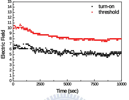
gallium nitrate concentrations ... 52 Figure 3-11 Stability of Eon and Eth of as-grown nanorod array ... 53
Figure 3-12 Stability of Eon and Eth of Ga-doped ZnO nanorods with gallium
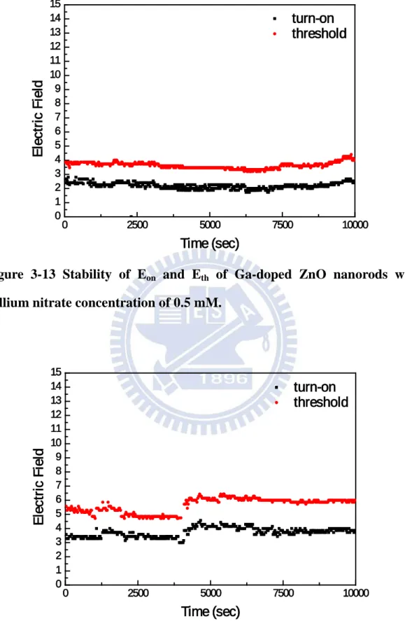
nitrate concentration of 0.1 mM ... 53 Figure 3-13 Stability of Eon and Eth of Ga-doped ZnO nanorods with gallium
nitrate concentration of 0.5 mM ... 54 Figure 3-14 Stability of Eon and Eth of Ga-doped ZnO nanorods with gallium
nitrate concentration of 1.0 mM ... 54 Figure 3-15 Stability of β value of as-grown ZnO nanorod array ... 55 Figure 3-16 Stability of β value of Ga-doped ZnO nanorods with gallium nitrate
X
concentration of 0.1 mM ... 55 Figure 3-17 Stability of β value of Ga-doped ZnO nanorods with gallium nitrate
concentration of 0.5 mM ... 56 Figure 3-18 Stability of β value of Ga-doped ZnO nanorods with gallium nitrate
concentration of 1.0 mM ... 56 Figure 3-19 1st, 100th, 200th, and 400th cycles measurement of J-E curves of as-grown nanorod array ... 57 Figure 3-20 1st, 100th, 200th, and 400th cycles measurement of J-E curves of Ga-doped
ZnO nanorods with gallium nitrate concentration of 0.1 mM ... 57 Figure 3-21 1st, 100th, 200th, and 400th cycles measurement of J-E curves of Ga-doped
ZnO nanorods with gallium nitrate concentration of 0.5 mM ... 58 Figure 3-22 1st, 100th, 200th, and 400th cycles measurement of J-E curves of Ga-doped
ZnO nanorods with gallium nitrate concentration of 1.0 mM ... 58 Figure 3-23 SEM images of oxygen plasma-treated ZnO nanorods with different
bombardment times under 10-1 torr (a) 0 second; (b) 30 seconds; (c) 60 seconds; (d) 90 seconds ; (e) 120 seconds ; (f) 150 seconds ... 59 Figure 3-24 SEM images of oxygen plasma-treated ZnO nanorods with different
bombardment times under 5×10⁻² torr (a) 0 second; (c) 30 seconds; (e) 60 seconds; (g) 120 seconds. (b)(d)(f)(h) are corresponding high
magnification ... 60 Figure 3-25 XRD patterns of oxygen plasma-treated ZnO nanorods with different
bombardment times ... 61 Figure 3-26 TEM analyses of ZnO nanorod with bombardment time for 60 seconds
(a) HR-TEM; (b) SAED; (c) EDS ... 62 Figure 3-27 Room-temperature PL spectra of oxygen plasma-treated ZnO nanorods
with different bombardment times ... 63 Figure 3-28 Visible regions for Room-temperature PL spectra of oxygen
XI
plasma-treated ZnO nanorods with different bombardment times ... 63 Figure 3-29 Field emission J-E curves of oxygen plasma-treated ZnO nanorods with
different bombardment times ... 64 Figure 3-30 Field emission F-N plots of oxygen plasma-treated ZnO nanorods with
different bombardment times ... 64 Figure 3-31 Stability of Eon and Eth of oxygen plasma-treated ZnO nanorods with
bombardment time for 30 seconds ... 65 Figure 3-32 Stability of Eon and Eth of oxygen plasma-treated ZnO nanorods with
bombardment time for 60 seconds ... 65 Figure 3-33 Stability of Eon and Eth of oxygen plasma-treated ZnO nanorods with
bombardment time for 120 seconds ... 66 Figure 3-34 Stability of β value of oxygen plasma-treated ZnO nanorods with
bombardment time for 30 seconds ... 66 Figure 3-35 Stability of β value of oxygen plasma-treated ZnO nanorods with
bombardment time for 60 seconds ... 67 Figure 3-36 Stability of β value of oxygen plasma-treated ZnO nanorods with
bombardment time for 120 seconds ... 67 Figure 3-37 1st, 100th, 200th, and 400th cycles measurement of J-E curves of oxygen
plasma-treated ZnO nanorods with bombardment time for 30 sec ... 68 Figure 3-38 1st, 100th, 200th, and 400th cycles measurement of J-E curves of oxygen
plasma-treated ZnO nanorods with bombardment time for 60 sec ... 68 Figure 3-39 1st, 100th, 200th, and 400th cycles measurement of J-E curves of oxygen
plasma-treated ZnO nanorods with bombardment time for 120 sec ... 69 Figure 3-40 SEM images of sharp Ga-doped ZnO nanorods ... 69 Figure 3-41 Room-temperature PL spectra of as-grown and sharp Ga-doped ZnO
nanorod arrays ... 70 Figure 3-42 Field emission J-E curves of ZnO nanorod arrays with different treated
XII
processes ... 70 Figure 3-43 Field emission F-N plots of ZnO nanorod arrays with different treated
processes ... 71 Figure 3-44 Stability of Eon and Eth of sharp Ga-doped ZnO nanorod arrays ... 71
Figure 3-45 Stability of β value of sharp Ga-doped ZnO nanorod arrays ... 72 Figure 3-46 1st, 200th, 400th, and 800th cycles measurement of J-E curves of sharp
1
Chapter 1 Introduction
1.1 Basic Properties of Zinc Oxide
Zinc oxide (ZnO) is ΙΙ-VΙ group semiconductor with a hexagonal wurtzite structure as Figure 1-1. The lattice parameter of ZnO wurtzite structure is a = 0.325 nm and c = 0.521 nm. ZnO nanostructures have high melting point (up to 1975 ℃) and excellent thermal and chemical stability. In addition, ZnO materials are generally n-type semiconductors with typical carrier concentration of 1017 cm-3 because of oxygen vacancies or zinc interstitials within them. The properties of ZnO are listed at Table1-1[1].
Recently, because of its direct wide band gap (3.4 eV) and large exciton binding energy (60 meV), ZnO nanostructures are recognized as a promising candidate for its application in functional nanodevice and nanotechnology such as ultraviolet light-emitting diodes[2] and ultraviolet laser[3]. ZnO is also well-known as a piezoelectric material in surface acoustic wave (SAW) devices for delay lines, filters, resonators in wireless communication, and signal processing because of its noncentrosymmetric structure[4]. Furthermore, ZnO is bio-safe and biocompatible, and may be used for biomedical devices[5] without coating.
In recent years, nanotechnology has been researched extensively. There are many kinds of nanostructures, including zero-dimension (0D) nanostructures such as nanoparticle[6], nanodot[7];one-dimension (1D) nanostructures such as nanowire[8], nanotube[9], nanorod[10,11,12] ; two-dimension (2D) nanostructures such as nanoblet[13], nanosheet[14]. Because of the special
2
morphology of nanostructures, there are many different properties compared to the bulk. It provides many new applications in electronic and optical devices.
Since the carbon nanotubes (CNTs) were discovered in 1991, one-dimensional semiconductor nanostructures such as nanorods, nanowires, and nanotubes have attracted much attention due to their many unique properties and the possibility. In addition to carbon, other one-dimension materials, like ZnO, GaAs and TiO2, were researched in recent years. Among them, ZnO nanorods exhibit not only large surface area and high aspect ratio but also many mentioned advantages of ZnO so that they may be used as ultraviolet laser[15], field emission display[16], gas sensor[17], hydrogen storage[18], and solar cell[19] etc. Figure 1-2 illustrates scanning electron microscopy (SEM) images of several ZnO nanostructures[20, 21, 22, 23, 24].
1.2 Field Emission Display
Various kinds of flat panel display devices such as liquid crystal display (LCD), vacuum fluorescent display (VFD), and plasma display panel (PDP), organic light emitting display (OLED) have been developed. Among them, LCD is the most popular flat panel displays. However, there are many drawbacks like low brightness, high cost, high temperature sensitivity, and narrow view angles in LCDs. Recently, more and more studies of flat panel display have been investigated lately. Field emission display (FED) especially attracts much more attention in these displays. FED is a vacuum electron device, sharing many common features with the cathode ray tube (CRT), including a glass vacuum envelope, phosphor coated anode, and a cathode electron source. Schematic diagram of CRT and FED are showed in Figure
3
1-3[25]. Just like in a CRT, the image in a FED is created by injecting electrons from a cathode onto a phosphor coated screen. In a CRT, the electron source is made up of up to three thermionic cathodes. A set of electromagnetic deflection coils can control electrons to scan the phosphor screen, which is typically held at a potential of 15~30 kV. In a FED, the electron source consists of a matrix-addressed array of millions of cold emitters. This field emission array (FEA) is placed above phosphor faceplate 0.2~2.0 (um) and is aligned such that each phosphor pixel has a dedicated set of field emitters. Thin panel thickness (approximately 2 (mm)), high image quality, wide view angle (about 170°), quick response (about uS), low power consumption, and high tolerance to environments are all advantages of FED.
Since 1960s, the concepts of FED were demonstrated, and many kinds of cathode emitters have been researched. Spindt successfully fabricated emitters of FED by semiconductor technology, called the Spindt-type cold cathode. Schematic diagram of Spindt-type cold cathode is showed in Figure 1-4[26]. The Spindt-type cold cathode is micro-meter scale emitters with self-aligned metal pyramids and gates. The metal pyramids are usually molybdenum with diameter of 1 (um). The advantage of Spindt-type cold cathode includes long lifetime, high brightness, and high adequate color purity. However, Spindt-type FED is high cost and its applicable size is not large enough. Other kinds of cathode emitters such as ballistic electron surface emitting device (BSD)[27], metal insulator metal (MIM)[28], surface conduction emitter (SCE)[29] and carbon nanotube (CNT)[30] emitter have been developed. The CNT emitters have been able to replace the metal pyramids of Spindt-type cold cathode recently. The structure of FED with carbon nanotube emitters is shown in
4
Figure 1-5[30]. However, the synthesis of CNTs is not only hard but also high temperature process. In addition, the chemical property of CNTs is unstable. As compared with CNTs, ZnO nanorods are easy to synthesize large scale by low temperature process. Low cost of synthesis and stable chemical property are also the advantages of ZnO nanorods. Therefore, we replace CNTs with ZnO nanorods as cathode emitters in this thesis.
1.3 Synthesis of Zinc Oxide Nanorods
ZnO nanorods can be synthesized by different methods such as vapor-liquid-solid (VLS) method, vapor solid method, thermal evaporation, metal-organic chemical vapor deposition (MOCVD), template-based synthesis, hydrothermal method, etc.
Vapor-Liquid-Solid (VLS) Growth Method
[31,32]
The VLS growth process was originally developed by Wagner and Ellis to produce micrometer-sized whiskers in 1964. This mechanism can be divided into two main steps: the formation of small liquid droplet and alloying, nucleation, and growth of the nanorods. In a typical VLS growth method, ZnO powder and graphite are mixed appropriately and load into an alumina boat, then the boat is placed in the center of a quartz tube under N2 or Ar flow. As the temperature is increased to the reactive temperature, the ZnO reacts with graphite to form Zn(g) and CO(g). The gaseous products produced by reactions (1.1) and (1.2) would adsorb and condense on the metal catalytic droplets. The nucleation is starting and the single crystalline ZnO nanorods grow by the reaction (1.3). The VLS growth method is easy to obtain nanorods with long
5
length and high aspect ratio. However, the high reaction temperature and catalysts metal are issues when the process integrals to VLSI process.
𝐙𝐧𝐎(𝐬) + 𝐂(𝐬) → 𝐙𝐧(𝐠) + 𝐂𝐎(𝐠) (𝟏. 𝟏)
𝐂𝐎(𝐠) + 𝐙𝐧𝐎(𝐬) → 𝐂𝐎
𝟐(𝐠) + 𝐙𝐧(𝐠) (𝟏. 𝟐)
𝐙𝐧(𝐠) + 𝐂𝐎(𝐠) → 𝐙𝐧𝐎(𝐬) + 𝐂(𝐬) (𝟏. 𝟑)
𝐂(𝐬) + 𝐂𝐎
𝟐(𝐠) → 𝟐 𝐂𝐎(𝐠) (𝟏. 𝟒)
Vapor Solid (VS) Growth Method
[33,34]
The growth mechanism works in a similar way to VLS process. However, VS do not need extra metal catalysts and the nanorods can deposition by thermally evaporating a suitable source material near its melting point at cooler temperature. The gaseous atoms play the role of the catalyst itself. In the VS growth mode, control of the nanorods diameter is accomplished by changing the evaporation, collection temperatures, and the vapor pressure. Although VS growth method can improve the disadvantage of VLS growth method, the aspect ratio and alignment of ZnO nanorods are worse than VLS.
Template-Based Synthesis
[35,36]
Template-based synthesis uses the porous Anodic Aluminum Oxide (AAO) substrate as the template of the ZnO nanorods. The AAO structure can provide some properties for nanorods, including high pores density, controllable diameter and length of pores, large area and uniform arrays. The holes of the AAO template are filled with ZnO by CVD, sol-gel or hydrothermal method. After filling the ZnO, NaOH solution is used to remove the AAO template.
6
Template-based synthesis is easy and cheap to synthesize ZnO nanorods, but it is not pure enough and hard to create single crystal ZnO nanorods. To strip template after nanorods growth is also a problem due to the process may damage the nanorod arrays.
Hydrothermal Growth Method
[37,38]
Hydrothermal growth method is a prevail method to synthesize ZnO nanorods. It has many advantages over other growth methods such as low cost, environmental friendliness, catalyst-free, large-scale production and low reaction temperature (below 100℃). Air flow is not considered to be used because the reaction is in the solution. For these advantages, ZnO nanorods are easier to integrate into the microelectronics and plastic electronics. The substrate with ZnO seeding layer which can help ZnO nanorods grow along C-orientation is put into an aqueous solution of zinc nitrate hexahydrate ( Zn(NO)3.6H2O ( 99.9% purity )) and the hexamethylenetetramine ( HMTA,
C6H12N4 ( 99.9% purity ) ) in a vessel. The zinc nitrate hexahydrate which is used as source of zinc and HMTA is used to control the pH value. The hydrothermal growth method can be shown in Figure 1-6. These can be represented by the following reactions:
(𝐂𝐇
𝟐)
𝟔𝐍
𝟒+ 𝟔𝐇
𝟐𝐎 → 𝟔𝐇𝐂𝐇𝐎 + 𝟒𝐍𝐇
𝟑(𝟏. 𝟓)
𝐍𝐇
𝟑+ 𝐇
𝟐𝐎 → 𝐍𝐇
𝟒++ 𝐎𝐇
−(𝟏. 𝟔)
𝟒𝐎𝐇
−+ 𝐙𝐧
𝟐+→ 𝐙𝐧(𝐎𝐇)
𝟒 𝟐−(𝟏. 𝟕)
𝐙𝐧(𝐎𝐇)
𝟒𝟐−→ 𝐙𝐧𝐎
(𝐒)+ 𝐇
𝟐𝐎 + 𝟐𝐎𝐇
−(𝟏. 𝟖)
7
The hydrothermal method is based on the formation of solid phase from a solution, which involves two steps: nucleation and growth. In the nucleation, the clusters of molecules are formed undergo rapid decomposition and particles combine to grow up to a certain thickness of the film by heterogeneous reactions on the substrate surface. When zinc nitrate tetrahydrate and HMTA are mixed together, no precipitation accrues initially. With the increase of reaction temperature, the HMTA begins to decompose into ammonia and the Zn(OH)2 occurs. For the solution is heated, ZnO nuclei are formed on the substrate. As soon as the ZnO nuclei are formed, the ZnO nanorods begin to grow. This synthesis of ZnO nanorods without catalysts or templates provides a promising option for the large-scale production of well-dispersed one-dimension nanostructure materials.
1.4 Field Emission Principle
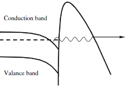
Field emission is a point discharge phenomenon. When we applied a negative voltage would induce a strong electric field near the tip of structures. The strong electric field would narrow and lower the potential barrier. Potential energy distribution from the emitter surface would become as Figure 1-7[40]. That causes more electrons to pass through this barrier and results in the current.
This phenomenon of electric tunneling is followed by Fowler-Nordheim tunneling[41]. This phenomenon is highly dependent on both the properties of materials and the shape of the particular cathodes. The field emission current density can be described by the F-N equation. The F-N equation[42] is as follow:
8
𝐉 =
𝐀𝛃
𝚽 𝐞𝐱𝐩 �−
𝟐𝐄
𝟐𝐁𝚽
𝟑 𝟐 �𝛃𝐄 � (𝟏. 𝟗)
𝛃 = 𝐒
𝐃
𝐑 (𝟏. 𝟏𝟎)
where J is the current density, E is the applied electric field of tip, Φ is the work function (ZnO is 5.37 eV), β is the field emission enhancement factor, A is 1.5×10⁻¹⁰ (AV-2eV), and B is 6.83×10³(eV-3/2V/um). From the Eq.1.9, we can know that the smaller work function and the higher electric field generate higher field emission current density. That is because the materials with smaller work function exhibit lower barrier height, then electrons can easily tunnel through this barrier. Higher electric field can also narrow and lower barrier height and enhance the probability of electron tunneling. Besides reducing work function, raising β can also generate higher field emission current density. The β can be written as Eq.1.10 where S is dependent on screen effect, D is the distance from anode to cathode, and R is dependent on the radius of electron emitter. If the neighboring emitters are farther, S is larger. It causes higher β and field emission current. The sharper morphology with smaller R can also contribute to higher β and emission current. In conclusion, the field emission current is highly dependent on both the properties of the material and the morphology[43] of the cathode. In this thesis, we would enhance the field emission property by lowering the work function of ZnO and narrowing the radius of the top of cathode emitter.
9
𝐥𝐧(
𝐄
𝐉
𝟐) = −
𝐁𝚽
𝟑 𝟐 �𝛃
𝟏
𝐄 + 𝐥𝐧(
𝐀𝛃
𝟐𝚽 ) (𝟏. 𝟏𝟏)
𝐦 = −
𝐁𝚽
𝟑 𝟐 �𝛃 (𝟏. 𝟏𝟐)
𝐛 = 𝐥𝐧(
𝐀𝛃
𝚽 ) (𝟏. 𝟏𝟑)
𝟐A plot of ln(J/E2) versus 1/E is a straight line with slope m and intercept b. The value of β can be calculated by Eq.1.12. Otherwise, the turn-on and threshold electric field (Eon and Eth) are also considered in field emission measurement. The Eon and Eth are defined as the electric field at the current density of 1.0 uA/cm2 and 1.0 mA/cm2. In this thesis, we judge the field emission properties of nanorods by Eon , Eth , and β. Larger β represents sharper tip structure and lower Eon and Eth can reduce the consumption of power.
1.5 Optical Properties of Zinc Oxide
ZnO generally reveals n-type conduction with a typical carrier concentration of 1017 cm-3, which is smaller than the carrier concentration of 1018 to 1020 cm-3 in ultraviolet light-emitting[44] and laser diode applications. Compared with other direct wide band gap materials, ZnO exhibits a larger exciton binding energy[45] (~60 meV) which assures more efficient exciton emission. In addition, the binding energy of ZnO is larger than its thermal energy (~26meV). For these reasons, ZnO has attracted considerable attention for optical applications such as ultraviolet light-emitting devices and optoelectronic devices. The optical spectrum is shown in Figure1-8[46].
10
mechanisms for the luminescence properties are still a matter of controversy. There are two general kinds of emission manners in ZnO. One is the ultraviolet emission (UV emission), and the other is the visible emission. The UV emission is related to the conduction band and valence band of zinc oxide, and The visible emission is related to the electron transition from the energy band of impurities and defects to the valence band. The optical properties of ZnO would be changed by dopant[47], structure, and annealing[48]. The mechanism of the ultraviolet and visible emission is shown in Figure1-9.
The UV emission is related to the exciton emission of ZnO. There is an exciton state under the conduction band within ZnO band diagram. External exciting energy would excite electrons from valence band to conduction band, and then electrons might jump to the exciton state. Finally, the electrons would spontaneously jump to the valence band, and release photons, energy and other forms of energy. In order to explain the visible emission in ZnO, various models have been proposed. According to the research of Vanheusden et al.[49], the visible emission originates from the oxygen vacancies. It concludes that the singly ionized oxygen vacancy center is the defect center for visible luminescence. There are three different oxygen vacancies that can be occurred in ZnO: the VΦ state which captures two electrons and is neutral relative to the lattice, the singly ionized VO‧ state which captures one electron, and the VO‧‧ state which do not trap any electron and is doubly positive charge relative to the lattice. In the main, the visible emission results from the recombination of the photogenerated hole in the valence band with the singly ionized oxygen vacancy. The more singly ionized oxygen vacancies are, the stronger visible luminescence intensity is. In this thesis, we would use oxygen plasma and dope
11
gallium to repair oxygen vacancies of ZnO nanorods, so that it can enhance the ratio of UV emission to visible emission.
1.6 Sharp Zinc Oxide Nanorods
It is well known that sharp ZnO nanorods can improve field emission property. In order to apply ZnO nanorods to field emission display (FED), we must fabricate sharp nanorods to lower turn-on electric field and reduce the consumption of operational power. Recently, many researchers have synthesized sharp ZnO nanorods by different methods[50] such as vapor phase transport and condensation (VPTC)[51] and chemical solution method[52]. For VPTC, the substrates are filled with metallic Zn powder. The substrates are positioned in different directions relative to the gas flow. Under the constant flow of argon at atmospheric pressure, the growth temperature is 450-600 ℃ and maintains it for 15 min ~ 1 hr. The morphologies of sharp nanorods are characterized as Figure1-10. For chemical solution method, sharp nanorods are fabricated by direct oxidation of zinc foil in alkaline zincates ion solution at room temperature. The morphologies of sharp nanorods are characterized as Figure1-11.
However, the VPTC procedures require higher temperature resulted in some limitations such as the choices of substrate and low product yield. Although chemical solution method is a low temperature process, it is limited by zinc foil substrate. In this thesis, we propose a physical process that as-grown ZnO nanorods are etched by oxygen plasma to improve the properties of field emission.
12
1.7 Doped Zinc Oxide Nanorods
It is well known that the dopants would change the electrical and photoluminescence properties of ZnO nanostructures. Nowadays, many researchers have been made to improve the properties of ZnO nanostructures by doping various chemical elements such as Al[53], In[54], Sn[55], Mg[56], and Ga[57] into ZnO lattice. Among these elements, gallium is an effective dopant for reducing the resistivity and less lattice distortion. Otherwise, gallium is less reactive and resistive to oxidation. Various methods have been reported to synthesize ZnO nanorods, including metalorganic chemical vapor deposition[58], thermal evaporation method[59], and PLD[60]. However, these methods require high temperature which results in some limitations in the application of FED and optical devices. In this thesis, we synthesis ZnO nanorods by the hydrothermal method which has the advantages of low temperature and large-scale product yield. The effects of gallium doping on the field emission and photoluminescence properties of ZnO nanorods are investigated.
13
property
value
Lattice parameter a
0(300K)
0.32495 nm
Lattice parameter c
0(300K)
0.52069 nm
Ratio c
0/a
01.602
Density
5.606 g/cm
3Stable phase at 300 K
Wurtzite
Melting point
1975℃
Thermal conductivity
0.6,1-1.2
Static dielectric constant
8.656
Refractive index
2.008
Energy gap
3.4 eV
Exciton binding energy
60 meV
Electron effective mass
0.24
Electron Hall mobility at 300 K
for low n-type conductivity
200 cm
2/V.s
Hole effective mass
0.59
Hole Hall mobility at 300 K
for low p-type conductivity
5-50 cm
2/V.s
14
Figure 1-1 Lattice structure of wurtzite ZnO
15
Figure 1-3 Schematic illustration of (a) CRT (b) FED structure
16
Figure 1-5 Structure of FED with carbon nanotube emitter
17
Figure 1-7 Potential energy distribution of emitter surface under electric field
18
Figure 1-9 Mechanism of ultraviolet and visible emission
19
Figure 1-11 SEM images of sharp ZnO nanorods synthesized by chemical solution
20
Chapter 2 Experimental Details
In this chapter, we will describe the experimental details of ZnO nanorods including sample preparation, measurement and analysis. The flow chart of experiment is shown in Figure 2-1.
2.1 Sample Preparation
2.1.1 Cleaning Wafer
In the experiment, the p-type Si (100) wafer is cleaned by a Standard Radio Corporation of America (RCA) cleaning method and rinsed in acetone for 30 minutes to remove native oxide and particles from the surface of Si substrate.
2.1.2 Deposition of ZnO Seeding Layer
ZnO nanorods are hard to grow on Si substrate due to lattice mismatch between Si and Zn. We should deposit the seeding layer to improve the growth rate. The seeding layer is deposited on Si wafer by spin coating. The chemical solution of spin coating is made of zinc acetate dihydrate (Zn(CH3COO)2.
2H2O (99.5% purity)) and ethanol absolute (C2H5OH (99.5% purity)) in a vessel, and then it is stirred for 1 hour at room temperature. The concentration of chemical solution is 0.005M. After dipping 3 ml solution on Si wafer, we spin coat for two spinning stages. The first stage is 720 rpm for 10 seconds and
21
the second stage is 2000 rpm for 30 seconds. Repeat above steps ten times. Finally, ZnO seeding layer is annealed at 320℃ for 30 min in the air atmosphere. Si wafer is cut into 2 cm × 2 cm substrates.
2.1.3 Growth of ZnO Nanorod Array
In this thesis, ZnO nanorod array grows by hydrothermal method. The Si substrate with ZnO seeding layer is put into an aqueous solution of zinc nitrate tetrahydrate (Zn(NO3)2. 4H2O (98% purity)) and hexamethylenetetramine
(HMTA; C6H12N4 (99.9% purity)) in a vessel at 90 ℃ for two hours. The concentrations of zinc and amine in the mixed solution are 0.05 M.
2.1.4 Growth of Ga-doped ZnO Nanorod Array
In this thesis, Ga-doped ZnO nanorods are synthesized by hydrothermal method. The Si substrate with ZnO seeding layer is put into an aqueous solution of zinc nitrate tetrahydrate (Zn(NO3)2 . 4H2O (98% purity)),
hexamethylenetetramine (HMTA ; C6H12N4 (99.9% purity)) and gallium nitrate hydrate (Ga(NO3)3.xH2O (99.9% purity)) in a vessel at 90 ℃ for two hours.
The concentrations of zinc and amine in the mixed solution are 0.05 M, and the concentration of gallium nitrate hydrate in the mixed solution fixes at 0.1, 0.5, 1.0 mM, respectively.
2.1.5 Fabrication of Sharp ZnO Nanorods
In this thesis, ZnO nanorods and Ga-doped ZnO nanorods are sharpened by oxygen plasma. For plasmatic etching, the substrates covered with ZnO
22
nanorod array are bonded on the sputtering target in a RF magnetron sputtering machine by carbon tape and are exposed to oxygen plasma with a RF power of 30 W under a pressure of 5×10⁻² torr. The etching process time of plasma treatment varies from 30 to 120 seconds. The structure of sharp nanorod array is shown in Figure 2-2.
2.2 Measurement and Analysis
2.2.1 Scanning Electron Microscopy (SEM)
Field emission scanning electron Microscopy (FESEM, Hitachi S4700) is used to observe the seeding layer surface morphology and the cross section of film thickness. Besides, it also observes the surface structure, morphology, diameter, length, and density of ZnO nanostructures. Hitachi S4700 operates at 15 kV under 2×10⁻⁶ torr with the solution of 1.5 nm. The cold field electron gun is used as the source of electron beam with the extraction voltage of 15 kV. The working current is 10μA. The schematic illustration of the SEM is shown in Figure 2-3.
2.2.2 Transmission Electron Microscopy (TEM)
The crystal structure and morphology analysis of ZnO nanorods can be measured by the high resolution transmission electron microscopy (HR-TEM, JEOL JEM-2100F). TEM is a microscopy technique whereby a beam of electrons is transmitted through a specimen, interacting with the specimen as it passes through it. An image is formed from the electrons transmitted through
23
the specimen, magnified and focused by an objective lens, and then detected by a sensor such as a CCD camera. And by the selected area electron diffraction (SAED), it can show the crystal structure of ZnO nanorod. The lattice constant of the ZnO nanorod can be observed by HR-TEM. Furthermore, in order to measure the other elements on ZnO nanorod array, the EDX of the TEM is used. The fixed quantity analysis of the EDX is also used for the quantity of Zn, O, and Ga. The schematic illustration of the TEM is shown in Figure 2-4.
The preparation of the TEM samples is through scratching the nanorods from the substrate, ultrasonic vibrating in ethanol and dripping the solution on the copper grid. The rate of the vibration is about 14000 rpm and the vibration time is 3~5 minutes.
2.2.3 X-ray Diffraction (XRD)
The crystal structure of ZnO nanorod array can be observed by the high resolution X-ray diffraction (XRD, Bede, D1). The X-ray diffraction equipment is often used for identifying the crystal structure. If the angle θ (Braggle’s angle) between the crystal plane and the incident light matches the Braggle’s law (nλ=2dsinθ), the incident light would be diffracted by the crystal plane. And then the reflected X-rays from the respective atomic planes can be measured by the detector. In the Braggle’s law, nλ is an integral number of wavelengths, and d is the distance between two successive crystal planes. The average grain size and orientations can be determined from XRD data. The schematic illustration of the X-ray diffraction is shown in Figure 2-5. The average grain size of a specimen is estimated from XRD peaks using Scherrer’s formula by
24
𝐃 =
𝐁 × 𝐜𝐨𝐬𝛉 (𝟐. 𝟏)
𝟎. 𝟗 × 𝛌
Where λ is the X-ray wavelength, B means the full width at half maximum of the XRD peak, abbreviated as FWHM, and θ is taken as diffraction angle.
The X-ray diffraction measurement with Cu Kα radiation (λ=1.5418Å) is operated at 30 kV and 20 mA. In order to avoid the peak of silicon about 70°, the angle 2θ of measurement is from 30° to 60°. The sweeping rate is 4° per minute.
2.2.4 Photoluminescence (PL)
Photoluminescence spectroscopy is a contactless and nondestructive method of probing the luminescence properties of materials. The luminescence properties of ZnO nanorod array can be measured by the photoluminescence (PL, JEOL IHR320, Japan) with a 325 nm Helium-Cadmium laser beam as an excitation source at room temperature. From the analysis of photoluminescence (PL) spectrum, it can reveal the band structure and carrier transportation behaviors of solid materials, and the doping type and defects in materials. Laser beam impacts on the sample, where it is absorbed and imparts excess energy into the material in a process called photo-excitation. When the laser beam illuminates the sample, the photo-excitation causes the electrons to jump from equilibrium state to excited state. Because the excited state is unstable, the electrons would subsequently return to the equilibrium state. Between the transitions of electrons, the redundant energy would release in the form of heat energy or photon energy. The photon energy would be measured by the detector.
25
The sweeping rate is 0.5 nm per second. The excited depth of electrical beam for ZnO material is several tens nanometer. The sweeping range is from 350 nm to 700 nm.
2.2.5 Field Emission Measurement
The field emission properties are measured in a high vacuum chamber. The chamber is maintained at a vacuum value of 5×10⁻⁶ torr at room temperature for whole measurement. The current-voltage (I-V) curves and field emission characteristics can be monitored by Keithley 237 equipment. A copper electrode probe, which is placed above the sample, is served as an anode with the area of 7.09×10⁻³ cm2, and ZnO nanorod array is served as the cathode. The measurement equipment is illustrated in Figure 2-6.
26
27
Figure 2-2 Structure of sharp ZnO nanorod array
Figure 2-3 Schematic illustration of the SEM
28
Figure 2-5 Schematic illustration of the X-ray diffraction
29
Chapter 3 Results and Discussion
3.1 ZnO Seeding Layer
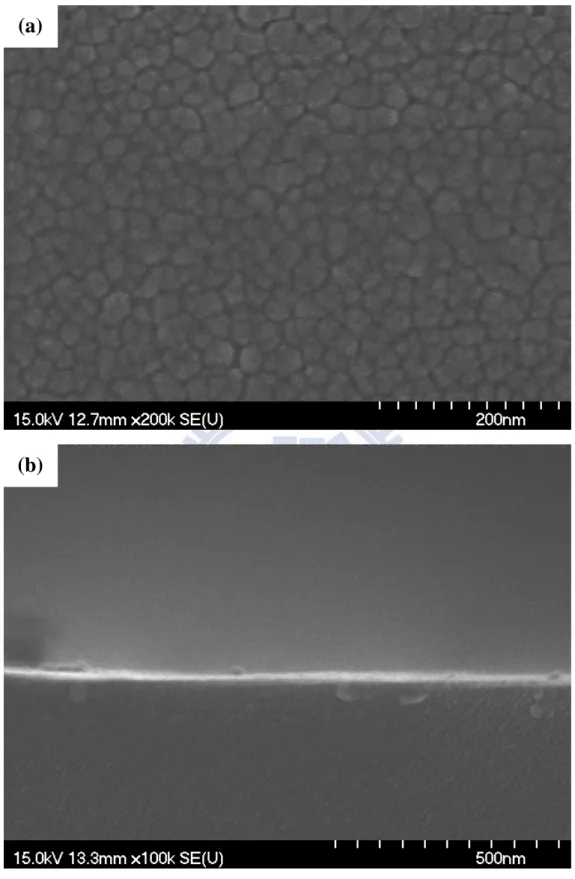
3.1.1 The SEM Analysis of Seeding Layer
Figure 3-1 shows the SEM images of ZnO seeding layer. Figure 3-1 (a) is the top view and Figure 3-1 (b) is the cross-section view. It can be observed that there are many grain boundaries on the ZnO seeding layer. The thickness of ZnO seeding layer which was deposited by spin-coating is about 24.3 nm. The thickness of ZnO seeding layer plays an important role to reduce the lattice mismatch between Si and ZnO. If the thickness of ZnO seeding layer is so thin that the large lattice mismatch would be difficult to synthesize well-aligned ZnO nanorod arrays. In conclusion, we succeeded to synthesize well-aligned ZnO nanorod arrays (as shown in the following sections) on the seeding layer which was deposited by spin-coating.
3.1.2 The XRD Analysis of Structure
Before synthesis of ZnO nanorod arrays, the ZnO seeding layer was deposited on Si wafer by spin-coating. Figure 3-2 shows the XRD pattern of ZnO seeding layer. The peak intensity of dominant (002) orientation is not obvious. Therefore, it can be observed that the seeding layer deposited by spin-coating is amorphous. However, the well-aligned ZnO nanorods can be synthesized on the ZnO seeding layer by hydrothermal method, even though
30
the seeding layer is amorphous. We will show the well-aligned nanorod arrays in the following sections.
3.2 Ga-doped ZnO Nanorod Array
Synthesis of Ga-doped Nanorods
Ga-doped ZnO nanorods were synthesized by hydrothermal method. In order to synthesize Ga-doped ZnO nanorod arrays, different quantities of gallium nitrate were dissolved in the solution of zinc nitrate tetrahydrate and hexamethylenetetramine to fix its concentration at 0.1, 0.5 and 1.0 mM, respectively.
3.2.1 The SEM Analysis of Morphology
Figure 3-3 shows the SEM images of undoped and Ga-doped ZnO nanorod arrays. It can be observed that small quantities of gallium nitrate would not significantly influence the lengths and diameters of ZnO nanorod arrays. However, for the 1.0 mM gallium nitrate solution as shown in Figure 3-3 (g) and (h), they show that there are obviously reductions of density, length, and diameter of ZnO nanorod arrays. Otherwise, the Ga-doped ZnO nanorods were in disorder. According to the reactions of hydrothermal method mentioned in Chapter 1, the reactions are shown as follow:
(𝐂𝐇
𝟐)
𝟔𝐍
𝟒+ 𝟔𝐇
𝟐𝐎 → 𝟔𝐇𝐂𝐇𝐎 + 𝟒𝐍𝐇
𝟑31
𝟒𝐎𝐇
−+ 𝐙𝐧
𝟐+→ 𝐙𝐧(𝐎𝐇)
𝟒𝟐−
𝐙𝐧(𝐎𝐇)
𝟒𝟐−→ 𝐙𝐧𝐎
(𝐒)+ 𝐇
𝟐𝐎 + 𝟐𝐎𝐇
−As the concentration of gallium nitrate increasing, the additional gallium ions prefer to react with OH− in the chemical solution. This reaction results in the reduction of ZnO precursor. Therefore, the density of ZnO nanorod arrays would decrease as the gallium nitrate concentration increasing.
3.2.2 The XRD Analysis of Structure
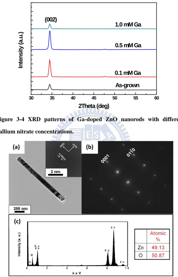
Figure 3-4 shows the XRD patterns of Ga-doped ZnO nanorod arrays with different gallium nitrate concentrations. It indicates that the intensity of orientation (002) direction is still very strong due to well-aligned ZnO nanorod arrays. Otherwise, the angle of (002) direction shifts to high angle (from 34.5° to 34.7°), because the ionic radius of gallium ion is smaller than that of zinc ion. But the (002) orientation peak of Ga-doped ZnO nanorod array with 1.0 mM doping concentration is obviously weaker. We conclude that additional gallium ions may cause lattice distortion results in reducing the intensity of orientation (002) direction.
3.2.3 The TEM Analysis of Structure
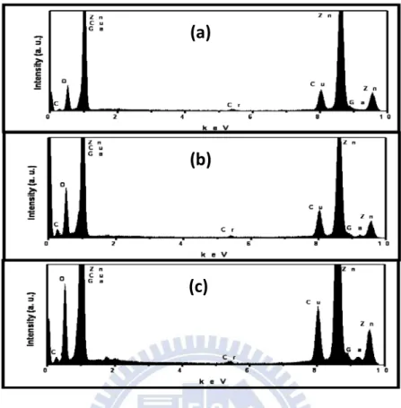
Figure 3-5 shows the TEM analyses of as-grown ZnO nanorod. As shown in the insert of Figure 3-5 (a), the ZnO nanorod is single crystalline structure. The average atomic spacing along the growth direction is about 0.52 nm, corresponding to a lattice spacing of the (0001) planes of wurtzite ZnO. From
32
the SAED image, it also illustrates that the growth direction of ZnO nanorod is along [0001]. The EDS analyses of Ga-doped ZnO nanorod with different gallium nitrate concentrations are shown in Figure 3-6. It shows that as increasing the gallium nitrate concentration, the quantity of gallium ions in the ZnO nanorod would increase. Further, we figured out the difference between experimental values and theoretical values. The statistical chart is shown in Figure 3-7. There is no significant difference between them. Therefore, we can assure that gallium ions were doped into ZnO nanorods by hydrothermal method.
3.2.4 The PL Spectrum of Structure
The room-temperature PL spectra of Ga-doped ZnO nanorod arrays with different gallium nitrate concentrations are shown in Figure 3-8. It indicates that the red-shift of the UV peak emission position (from 378 nm to 380 nm) with doping gallium ions into ZnO nanorods. It is known that, when ZnO is doped with gallium, the excess carriers supplied by the impurities to the conduction band contribute to increase electrical conductivity of ZnO and thus leads to a red-shift of the UV peak[61]. Otherwise, the broad visible emission is quenched with gallium doping. It is known that Zn interstitials and oxygen vacancies are the common defects in ZnO, which are relative to visible emission. Therefore, the intensity of visible emission decays, demonstrating that the native defects are quenched due to gallium doping. It would enhance the ratio of IUV to IVisible.
33
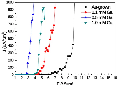
Figure 3-9 shows the J-E curves of undoped and Ga-doped ZnO nanorod arrays. The corresponding F-N plots are shown in Figure 3-10. The parameters of field emission properties with different doping concentrations are listed in Table 3-1. According to previous papers, doping gallium into ZnO nanorods reduces the resistivity because of much higher carrier concentration and mobility. The reduction of resistivity can reduce the voltage drop along ZnO nanorod, resulting in enhancement of the effective filed at the ZnO nanorod. Otherwise, the n-type doping can increase the possibility of electrons tunneling by lifting the Fermi level and lowering the work function of the ZnO nanorods. We measured the carrier concentration (as listed in Table 3-1) by Hall Effect measurement. According to Xu, C. X., et al.[62], we can calculate out that work functions of Ga-doped ZnO nanorod arrays with 0.1 mM, 0.5 mM, and 1.0 mM gallium nitrate concentrations are 4.65 (eV), 4.57 (eV), and 4.56 (eV), respectively. For the 0.5 mM gallium nitrate solution, it shows the best field emission properties. The turn-on field (Eon) and threshold field (Eth) are 2.67 (V/um) and 3.87 (V/um), respectively. And the field enhancement factor (β) is 1904.77. However, additional gallium ions would suppress the synthesis of ZnO nanorods and reduce the aspect ratio of ZnO nanorods, so that they would deteriorate the field emission properties. In conclusion, the field emission measurements confirm that the Ga-doped ZnO nanorod arrays have lower turn-on field, lower threshold field and larger field enhancement factor with higher current density, compared to the as-grown ZnO nanorod array.
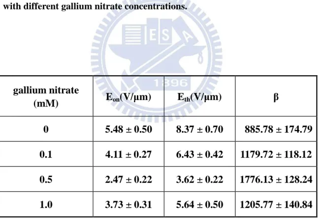
3.2.6 The Stability of Field Emission Measurement
34
properties are measured for 10000 seconds. Figure 3-11 to Figure 3-14 show the stabilities of turn-on field and threshold field of as-grown and Ga-doped ZnO nanorod arrays. The corresponding stabilities of field enhancement factor (β) are shown in Figure 3-15 to Figure 3-18. The details of field emission properties with different doping concentrations are listed in Table 3-4. In the Table 3-4, we can know that appropriate doping concentration would improve the stability of field emission properties. We may suggest that Ga-doped ZnO nanorods have higher crystal quality (as shown in XRD pattern). However, for the gallium nitrate concentration of 1.0 mM, the stability of Ga-doped ZnO nanorod array is deteriorated. We may conclude that it is related to the reason that ZnO nanorods are in disorder. Disordered ZnO nanorods are not all well-aligned, so that tops of ZnO nanorod emitters would not all point to the same direction. Therefore, disordered ZnO nanorod arrays would worsen the stability of field emission. Furthermore, we tested the cycle measurement. It can truly show the overall stability. The J-E curves of Ga-doped ZnO nanorods with different gallium nitrate concentrations in the 1st, 100th, 200th, and 400th cycles measurements are shown in Figure 3-19 to Figure 3-22. It is shown that the J-E curves of Ga-doped ZnO nanorods are less variation than that of as-grown ZnO nanorods. In conclusion, the Ga-doped ZnO nanorod arrays exhibit better stability than that of as-grown ZnO nanorod array.
3.3 Sharp ZnO Nanorod Array
Fabrication of Sharp Nanorods
35
solution for 2hr at 90 ℃ with different bombardment times. The RF power was fixed at 30W and the pressure of vacuum chamber was under 10-1 and 5×10⁻² torr.
3.3.1 The SEM Analysis of Morphology
Figure 3-23 shows the SEM images of oxygen plasma-treated ZnO nanorod arrays with different bombardment time varies from 30 to 150 seconds under 10-1 torr. It indicates that the nanorod arrays could not be significantly sharpened under 10-1 torr. Because the pressure of vacuum chamber was not low enough, we lowered the pressure down to 5×10⁻² torr. Figure 3-24 shows the SEM images of oxygen plasma-treated ZnO nanorod arrays with different bombardment time varies from 30 to 120 seconds under 5×10⁻² torr. For the plasma-treated time for 30 seconds, the edge of nanorod top started to be rounded by ion bombardment. It indicates that the nanorod arrays could be indeed sharpened by oxygen plasma-treated process under 5×10⁻² torr. For the plasma-treated time for 60 seconds, the morphology of nanorod top became cone-like. The top of nanorod with plasma-treated time for 60 seconds is the sharpest and smoothest compared to those with other bombardment times. However, for the plasma-treated time for 120 seconds, the angle of nanorod top became lager and the edge of nanorod top became rounder. Otherwise, there is an obvious reduction of nanorod length after ion bombardment for 120 seconds. The shorter and rounder nanorod arrays would deteriorate the field emission properties. In Figure 3-24, it also can be observed that the nanorod arrays still maintain perpendicular to the substrate after ion bombardment. Importantly, we should control the bombardment time to fabricate the best sharp morphology of
36
ZnO nanorod arrays which are applied to field emission display. In conclusion, the morphology of oxygen plasma-treated ZnO nanorod arrays with ion bombardment time for 60 seconds is the sharpest and smoothest morphology.
3.3.2 The XRD Analysis of Structure
Figure 3-25 shows the XRD patterns of oxygen plasma-treated ZnO nanorod arrays with different bombardment time varies from 30 to 120 seconds under 5×10⁻² torr. The (002) peak is the strongest due to its orientation of ZnO nanorods growth. It can be observed that the (002) orientation of nanorods became stronger with increasing the bombardment time. It indicates that the structure was stronger and crystal quality was better after oxygen plasma-treated process. In conclusion, the oxygen plasma-treated process can improve the structure and crystal quality of ZnO nanorod arrays.
3.3.3 The TEM Analysis of Structure
Figure 3-26 shows the TEM analyses of ZnO nanorod with bombardment time for 60 seconds. From the Figure 3-26 (a), it illustrates that the top of ZnO nanorod is sharp. The inserts of Figure 3-26 (a) are the HR-TEM images of side and tip of ZnO nanorod, respectively. These images illustrate that the ZnO wurtzite structure is complete without destruction. It concludes that there is no significant change on the surface crystal structure after oxygen plasma-treated process. From the SAED image, the atomic spacing along the growth direction is about 0.52 nm, corresponding to a lattice spacing of the (002) planes of wurtzite ZnO. Furthermore, the EDS analysis shows that the content ratio of zinc to oxygen is close to 1, consistent with the theoretical value.
37
3.3.4 The PL Spectrum of Structure
Figure 3-27 shows the room-temperature PL spectra of oxygen plasma-treated ZnO nanorod arrays with different bombardment time varies from 30 to 120 seconds under 5×10⁻² torr. The corresponding visible region for PL spectra of oxygen plasma-treated ZnO nanorod arrays with different bombardment times are shown in Figure 3-28. The PL spectra show a sharp UV emission, which is generated by the free-exciton recombination at 378 nm. A broad visible emission, which is caused by impurities and structural defects, is observed from 500 to 600 nm. It also can be observed that the intensity of the UV emission increased after the oxygen plasma-treated process, while the intensity of the visible emission decreased. It is well known that the ZnO nanorods which are synthesized by the hydrothermal method have many defects such as oxygen vacancies and Zn interstitials due to low temperature process (below 100℃). From the PL spectra, we can know that the intensity of visible emission decreased and the ratio of IUV to IVisible was raised after oxygen plasma-treated process. We may conclude that oxygen ions can be implanted into ZnO to fill in the oxygen vacancies during oxygen plasma-treated process. It results in good crystal quality and less defects on the surface. Moreover, the UV emission is associated with the quantity of free excitons. According to Hsieh, P. T., et al.[63], the oxygen atmosphere can improve the crystallinity of ZnO and increase amount of free excitons. Therefore, the intensity of UV emission can be stronger with increasing the bombardment time. In conclusion, the oxygen plasma-treated ZnO nanorods can effectively reduce the intensity of visible emission and enhance the ratio of IUV to IVisible.
38
3.3.5 The Field Emission Measurement
Figure 3-29 shows the J-E curves of oxygen plasma-treated ZnO nanorod arrays with different bombardment time varies from 30 to 120 seconds under 5×10⁻² torr. The corresponding F-N plots are shown in Figure 3-30. The parameters of field emission properties of ZnO nanorod arrays with different bombardment times are listed in Table 3-3. It well known that turn-on field (Eon), threshold field (Eth) and field enhancement factor (β) are dependent on morphology, aspect ratio and work function. According to Table 3-3, the oxygen plasma-treated ZnO nanorod arrays with bombardment time for 60 seconds show the best field emission properties. The turn-on field and threshold field are 2.43 (V/um) and 3.61 (V/um), respectively. And the β value is 2267.68. The oxygen plasma-treated ZnO nanorod arrays with bombardment time for 60 seconds exhibit the lowest turn-on field and threshold field and the largest field enhancement factor of all. It is because the top of nanorod is the sharpest and smoothest than others. Otherwise, some researches[64] mention that oxygen-treated process can lower the work function of ZnO. However, the decrement of work function is small. Therefore, we think that sharp morphology would be the main factor to improve the field emission properties, so that we do not take the influence of wok function into consideration. In addition, the oxygen plasma-treated ZnO nanorod arrays with different bombardment time exhibit better field emission properties than as-grown ZnO nanorod arrays. In our results, nanorods with oxygen plasma-treated process can improve field emission properties.
39
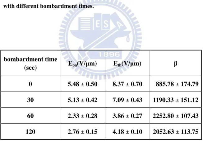
3.3.6 The Stability of Field Emission Measurement
Figure 3-31 to Figure 3-33 show the stabilities of turn-on field and threshold field of oxygen plasma-treated ZnO nanorod arrays with different bombardment times. The corresponding stabilities of field enhancement factor are shown in Figure 3-34 to Figure 3-36. The details of stability of field emission properties of ZnO nanorod arrays with different bombardment times are listed in Table 3-4. It can be observed that the turn-on field and threshold field of plasma-treated nanorod arrays were more stable than those of as-grown nanorod arrays. Otherwise, the oxygen plasma-treated nanorod arrays exhibit stable β values. We may suggest that plasma-treated nanorod arrays have better crystal quality and stronger structure, which are proved in XRD analysis, than as-grown nanorod arrays. Good quality and strong structure are good to resist high field. In addition, another reason for better stability is that the nanorod with sharp morphology generates current at its apex during the measurement. The J-E curves of oxygen plasma-treated ZnO nanorods with different bombardment times in the 1st, 100th, 200th, and 400th cycles measurements are shown in Figure 3-37 to Figure 3-39. It is observed that oxygen plasma-treated ZnO nanorod arrays indeed exhibit more stable than as-grown ZnO nanorod array. In conclusion, oxygen plasma-treated process can improve the stability of field emission properties of ZnO nanorod arrays.
3.4 Sharp Ga-doped ZnO Nanorod Array
40
In the section 3.2 and section 3.3, we know that the sharp nanorod arrays with bombardment time for 60 seconds exhibit the best properties of field emission in the oxygen plasma-treated process. Otherwise, the Ga-doped ZnO nanorod arrays with doping concentration of 0.5 mM also exhibit the best parameters of field emission in the doping process. Therefore, in this section, we synthesized the sharp Ga-doped ZnO nanorod array to investigate the properties of field emission. First, we synthesized the Ga-doped ZnO nanorod array with gallium nitrate concentration of 0.5 mM by hydrothermal method. Then, the Ga-doped ZnO nanorod array was etched by oxygen plasma with bombardment time for 60 seconds. The RF power was fixed at 30W and the pressure of vacuum chamber was under 5×10⁻² torr. Finally, the sharp Ga-doped ZnO nanorod array was well-done.
3.4.1 The SEM Analysis of Morphology
Figure 3-40 shows the SEM images of sharp Ga-doped ZnO nanorod array. It indicates that the Ga-doped ZnO nanorods can be easily sharpened by oxygen plasma-treated process in the same plasma-treated condition. The doped ZnO nanorods would not influence the fabrication of sharp morphology during the oxygen plasma-treated process. And the parameter of c/a would not be change obviously.
3.4.2 The PL Spectrum of Structure
The room-temperature PL spectra of as-grown and sharp Ga-doped ZnO nanorod arrays are shown in Figure 3-41. The PL spectra match with previous PL spectra in section 3.2.3 and section 3.3.3. The UV peak emission is shifted
41
from 378 nm to 380 nm due to gallium doping, and intensity of visible emission is reduced by oxygen plasma-treated process. It also can enhance the ratio of IUV to IVisible. Therefore, we can use oxygen plasma-treated process to repair oxygen vacancies to effectively improve optical characteristics of ZnO nanorod arrays.
3.4.3 The Field Emission Measurement
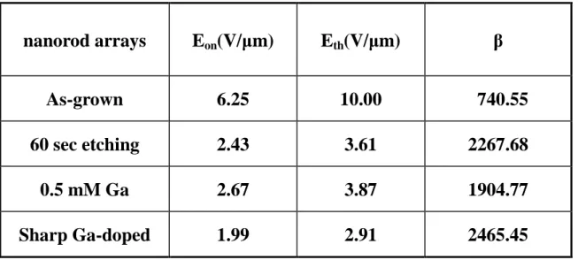
The J-E curves of ZnO nanorod arrays with different treated processes are shown in Figure 3-42. The corresponding F-N plots are shown in Figure 3-43. The details of field emission properties with different treated processes are listed in Table 3-5. As shown in the Table 3-5, the J-E plot demonstrates that Ga-doped nanorod array is the best candidate for field emission display with the lowest turn-on field and threshold field of 1.99 (V/cm) and 2.91 (V/cm), respectively. In addition, the β value of sharp Ga-doped nanorod array is the largest of all. It is because that the sharp morphology due to oxygen plasma-treated process and lower work function due to dope gallium ions are all factors to improve field emission properties. Therefore, we can effectively enhance field emission properties by doping process and oxygen plasma-treated process.
3.4.4 The Stability of Field Emission Measurement
Furthermore, to research the stabilities of sharp Ga-doped nanorod array, we measured the stabilities of field emission properties for 20000 seconds. Figure 3-44 shows the stabilities of turn-on field and threshold field of ZnO nanorod arrays with two-step treated processes. The corresponding stability of
42
field enhancement factor (β) is shown in Figure 3-45. The details of field emission properties with different treated processes are listed in Table 3-6. The average turn-on field and threshold field are 2.01 (V/um) and 3.00 (V/um), respectively. The corresponding standard deviations are 0.09 and 0.10, respectively. The average field enhancement factor is 2440.22, and the corresponding standard deviation is 108.77. They show that the sharp Ga-doped ZnO nanorod array exhibit the best stabilities on the whole. It is because that the nanorod with sharp top generated current at its apex during measurement. In addition, that the crystal quality is better after oxygen plasma-treated process is another factor to improve the stability of ZnO nanorod array. In addition, the J-E curves of sharp Ga-doped ZnO nanorods in the 1st, 200th, 400th, and 800th cycles measurements are shown in Figure 3-46. It also shows less variation of turn-on field and threshold field during the cycle measurement. Therefore, the sharp Ga-doped ZnO nanorod array indeed has better stability and lower power consumption for applying to field emission displays.
43
gallium nitrate
(mM)
E
on(V/
μm) E
th(V/
μm)
carrier
concentration
(cm
-3)
β
0
6.25
10.00
740.55
0.1
4.29
6.86
5.12×10
171133.44
0.5
2.67
3.87
5.89×10
181904.77
1.0
3.71
5.57
9.89×10
181320.99
Table 3-1 The details of field emission properties of ZnO nanorod arrays with different gallium nitrate concentrations.
gallium nitrate
(mM)
E
on(V/
μm)
E
th(V/
μm)
β
0
5.48 ± 0.50
8.37 ± 0.70
885.78 ± 174.79
0.1
4.11 ± 0.27
6.43 ± 0.42
1179.72 ± 118.12
0.5
2.47 ± 0.22
3.62 ± 0.22
1776.13 ± 128.24
1.0
3.73 ± 0.31
5.64 ± 0.50
1205.77 ± 140.84
Table 3-2 The details of stability of field emission properties of ZnO nanorod arrays with different gallium nitrate concentrations.
44
bombardment time
(sec)
E
on(V/
μm)
E
th(V/
μm)
β
0
6.25
10.00
740.55
30
5.17
6.83
1012.22
60
2.43
3.61
2267.68
120
3.00
4.14
1824.38
Table 3-3 The details of field emission properties of ZnO nanorod arrays with different bombardment times.
bombardment time
(sec)
E
on(V/μm)
E
th(V/μm)
β
0
5.48 ± 0.50
8.37 ± 0.70
885.78 ± 174.79
30
5.13 ± 0.42
7.09 ± 0.43
1190.33 ± 151.12
60
2.33 ± 0.28
3.86 ± 0.27
2252.80 ± 107.43
120
2.76 ± 0.15
4.18 ± 0.10
2052.63 ± 113.75
Table 3-4 The details of stability of field emission properties of ZnO nanorod arrays with different bombardment times.