國 立 交 通 大 學
電信工程學系碩士班
碩 士 論 文
應用於超寬頻脈衝通訊系統之接收機前端電路設計
與實現
A Front-End Receiver Design and Implementation for Impulse
Radio Ultra-Wideband Communication Systems
研 究 生:謝明憲 (Ming-Hsien Hsieh)
指導教授:陳富強 博士 (Dr. Fu-Chiarng Chen)
應用於超寬頻脈衝通訊系統之接收機前端電路設計與實現
A Front-End Receiver Design and Implementation for Impulse Radio
Ultra-Wideband Communication Systems
研 究 生 : 謝明憲 Student : Ming-Hsien Hsieh
指導教授
: 陳富強 博士 Advisor : Dr. Fu-Chiarng Chen
國 立 交 通 大 學
電 信 工 程 學 系 碩 士 班
碩 士 論 文
A Thesis
Submitted to Department of Communication Engineering
College of Electrical and Computer Engineering
National Chiao Tung University
in partial Fulfillment of the Requirements
for the Degree of
Master
in
Communication Engineering
September 2007
Hsinchu, Taiwan, Republic of China
應用於超寬頻脈衝通訊系統之接收機前端電路設計與實現
研究生:謝明憲 指導教授:陳富強 博士
國立交通大學 電信工程學系碩士班
摘 要
在本論文研究中,將針對脈衝超寬頻的低功率、低複雜度架構之特性,設計出 適用於脈衝超寬頻通訊系統之接收機前端電路。首先各別設計低雜訊放大器及相關 器。低雜訊放大器方面採用變壓器作輸入匹配,由於反向變壓器之電感隨著頻率增 加而變小,經小訊號模型推導後發現可將此特性應用在寬頻匹配上。另外在增益級 部分運用電流再利用技巧達到低功耗、高增益之特性。經量測後得到在3.1~10.6GHz 輸入反射損耗S11<-9.8dB,平均順向增益 S21=11.2dB,且頻帶內變異為 1.2dB。最 低雜訊表現為 3.2dB。另外相關器是作為訊號偵測及解調之用,此次以吉伯特架構 作時域訊號相乘,並以電感產生零點作頻寬的延伸,再加上可調增益之機制。實際 量測得到輸出振幅為36-89mV,與模擬之可調範圍有些許差距。最後我們整合前端 電路在單一晶片上,其子電路包含低雜訊放大器、脈波產生器以及類比相關器三個 子電路。首先雙極性之開關式二階微分高斯脈波產生器,經模擬後得到脈波寬度約 為 260ps。而相關器有別於之前設計,此次乘法器是以四相位架構實現,目的是將 接收後經放大的訊號與脈波產生器產生當作本地訊號作相乘,並經過在差動輸出端 加上的跨接電容以完成積分,另外再串一級運算放大器,加上主極點消除技術以延伸頻寬,由於此技術所用之電容橫跨在運算放大器的輸入輸出級上,同樣亦具有積
分效果。整個接收電路經量測後適用在110Mbps 或更高之傳輸速率上,上升時間約
為 1.8ns,持續時間為 2.2ns。此高傳輸以及低功耗等特性證明可應用在超寬頻脈衝
A Front-End Receiver Design and Implementation for Impulse
Radio Ultra-Wideband Communication Systems
Student: Ming-Hsien Hsieh Advisor: Dr. Fu-Chiarng Chen
Department of Communication Engineering
National Chiao Tung University
ABSTRACT
In this thesis we focus on the characteristics of low power, low complex architecture and design of a front-end receiver used in IR-UWB communication systems. First of all, the LNA and correlator are designed separately. The wideband input matching of LNA is realized by the transformer feedback topology instead of multi-stage filters. Since the inductance of the inverting transformer degrades as frequency increases, this characteristic can be applied in wideband matching by means of small-signal model. As to gain stage, the current-reuse technique reduces power dissipation and obtains adequate gain simultaneously. The measured results in 3.1 to 10.6 GHz show that S11 is less than -9.8 dB, S21 is equal to 11.2 dB with 1.2 dB variation, the minimum NF is 3.2 dB. Further, the correlator used for detecting signal is realized by the Gilbert multiplier. Some mechanisms are developed for bandwidth extension and dynamic gain control. The practical measurement shows that the output amplitude is 36-89mV. The adjustable range is slightly different from that in simulation. Finally, the integrated front-end receiver is proposed. The single chip comprises three sub-blocks including a wideband LNA, a pulse
generator, and an analog correlator. The bi-phase, switched, 2nd derivative pulse generator can generate the pulse width of 260ps. The analog correlator is modified and different from the previous design. It utilizes a four-quadrant multiplier and integral capacitors to implement the design. Besides, we exploit zero-pole cancelling topology to reach bandwidth enhancement and doubly integration simultaneously. The whole front-end receiver can work functionally in 110Mb/s, and the rise time and hold time of the demodulated signal are about 1.8ns and 2.2ns, respectively. The features prove that it is suitable in IR-UWB communication systems.
ACKONWLEDGEMENTS
一轉眼兩年的研究所生活就要過去了,首先我要感謝我的指導教授陳富強博士 這兩年來對我耐心的指導與鼓勵,經常在我遇到瓶頸時給予不一樣的意見及方向, 平日也常教導我們作研究應有的態度與解決問題的能力,相信這些東西對往後的我 絕對是受用無窮的。當然我也要感謝這兩年來陪我一起努力的實驗室同伴,親切的 阿南學長總是不厭其煩的替我們解惑,並帶領我們這些學弟們使實驗室更上軌道。 而有著深厚數學底子及豐富業界經驗的濬朋學長也常給予我們寶貴的經驗。另外感 謝已畢業的阿德和敦元學長們,是你們教導我電路相關設計技巧以及下線流程應注 意事項。還有同屆的 Eric、邱仔和阿筆,大伙一同修課討論聚餐作研究甚至是一起 在實驗室大掃除的那段同甘共苦的日子是非常值得回憶的。而實驗室的學弟們-小潘、 士元、力元、小莊以及小高,有你們的加入、相信實驗室未來會更有活力、更具發 展,也期望往後你們能帶領著新加入的學弟們繼續努力下去。再來我也要感謝鴻耀、 子豪、士傑、憲瑞、進府等好朋友,常跟你們切磋及討論也讓我在 RF 電路方面學 習到不少。當然我也要感謝國家晶片系統設計中心(CIC)提供良好的下線服務和量測 環境以及小誠、源佳、峰哥、小簡、阿穀、恆茹等工程師的相關協助,使我能順利 完成這篇論文。 最後,我要非常地感謝我的父母對我的栽培及關心,對我的所作的決定總是站 在支持的立場,讓我能如期完成這兩年的學業。也謝謝我的哥哥在我研究生活上額 外的幫助和鼓勵,也希望我的努力可以成為弟弟的好榜樣,特別也要感謝從小疼愛 我的奶奶,僅以此小小的成果獻給我最敬愛的家人。CONTENTS
ABSTRACT (CHINESE)...I
ABSTRACT (ENGLISH)...III
ACKNOWLEDGEMENTS...V
CONTENTS...VI
FIGURE CAPTIONS...VIII
TABLE CAPTIONS...X
Chapter 1 Introduction...1
1.1 Motivation...1 1.2 Thesis Organization...2Chapter 2 Ultra-Wideband Communication System...3
2.1 Introduction...3
2.2 Impulse-Radio UWB Communication System...6
2.2.1 Definition...6
2.2.2 Features and Advantages...8
2.3 Pulse Shaping...10
2.4 Pulse Modulation...13
2.5 IR-UWB Receiver...15
Chapter 3 Design of the Ultra-wideband LNA and Correlator ...18
3.1 Overview...18
3.2 A UWB LNA with Transformer Feedback Matching Network...18
3.2.1 Introduction of Monolithic Transformers...18
3.2.3 Simulation and Measurement Results...23
3.2.4 Discussion...27
3.3 An Analog Correlator with Dynamic Gain Control...35
3.3.1 Design Concepts...35
3.3.2 Simulation and Measurement Results...40
3.3.3 Discussion...46
3.4 Conclusion...46
Chapter 4 An Integrated Front-end Receiver for IR-UWB Wireless
Communication Systems...48
4.1 Overview...48
4.2 Switched 2nd-order Gaussian Pulse Generator...49
4.3 Doubly-Integrated, Inductorless, Wideband Correlator... 53
4.4 Layout Consideration and Simulation Results...58
4.5 Measurement Results...61
4.5.1 Measurement Environment... 61
4.5.2 Measurement Results and Discussion... 62
Chapter 5 Conclusion and Future Works... 64
5.1 Conclusion...64
5.2 Future Works...65
FIGURE CAPTIONS
Figure 2-1 UWB spectrum mask for indoor communication systems………...………...4
Figure 2-2 Multi-band OFDM frequency band plan………5
Figure 2-3 DS-UWB operating band (a) low band (b) high band…………...…...……….6
Figure 2-4 Illustration of UWB……….…………...………7
Figure 2-5 Gaussian pulse and spectrum allocation………..……….………10
Figure 2-6 Gaussian monocycle and spectrum allocation………..………11
Figure 2-7 Scholtz’s monocycle and spectrum allocation………..………...………12
Figure 2-8 Spectrum allocations of higher-order derivatives of Gaussian pulses…….…12
Figure 2-9 (a) OOK (b) PAM……….………..……….…….13
Figure 2-10 BPSK………...…...………14
Figure 2-11 PPM………..………...…………...………14
Figure 2-12 Graphic form of time-hopping pulse position modulation…….………15
Figure 2-13 Architecture of the coherent receiver……….………17
Figure 2-14 Architecture of the non-coherent receiver………17
Figure 2-15 Performance curves of a non-coherent receiver and a coherent receiver using BPSK modulation………...…...………17
Figure 3-1 (a) Electrical model for an ideal transformer (b) Equivalent circuit of an integrated transformer………...…….………20
Figure 3-2 Monolithic transformer winding configurations (a) Parallel conductor winding (b) Interwound winding (c) Overlay winding (d) Concentric spiral winding………21
Figure 3-3 Schematic of the proposed UWB LNA………23
Figure 3-4 The simplified input impedance network………...………24
Figure 3-5 Gain performance with LB variation………..…………26
Figure 3-7 Microphotograph of the proposed LNA………...…………29
Figure 3-8 S11 simulation and measured results of UWB LNA…………...………29
Figure 3-9 S21 simulation and measured results of UWB LNA………...…………30
Figure 3-10 S12 simulation and measured results of UWB LNA……….…………30
Figure 3-11 S22 simulation and measured results of UWB LNA…………..…...………31
Figure 3-12 NF simulation and measured results of UWB LNA…………..………31
Figure 3-13 Measured input 1-dB compression point at 5GHz……….………32
Figure 3-14 Spectral diagram of the IIP3 measurement (one tone is 5GHz, and the other tone is 5.01GHz) …………..………..………...…………32
Figure 3-15 Measured P1dB and IIP3 curves over the UWB band…………..….………33
Figure 3-16 A Gilbert multiplier…………..………..……..……..………36
Figure 3-17 Schematic of the proposed correlator circuit…………..………37
Figure 3-18 The transconductance stage with source degeneration…………...…………38
Figure 3-19 (a) Gm-C-OTA integrators (b) The correlator with direct integration……39
Figure 3-20 Input waveforms……….………..……..………41
Figure 3-21 Simulation output waveforms …………..………...…..……41
Figure 3-22 Simulation (a) different output waveforms with variation ( =0.7V~ 1.8V) (b) output amplitude versus …………..…………..………...…….……42
ctrl V Vctrl ctrl V Figure 3-23 Simulation output amplitude versus input amplitude…………..……..……42
Figure 3-24 (a) The practical monocycle pulse generator (b) Measured waveforms …42 Figure 3-25 Photograph of the on-board chip with bonding wire …………..…………43
Figure 3-26 Measured single-end output waveforms (Vctrl = 1.8V) ………...….……43
Figure 3-27 Measured single-end output waveforms (Vctrl = 0.7V) ………...….………44
Figure 3-29 Microphotograph of the proposed correlator ………...….……45
Figure 4-1 System architecture of IR-UWB transceiver (dash line indicates RX front end)...49
Figure 4-2 Block diagram of the generation of the 2nd-order derivative Gaussian pulse..50
Figure 4-3 Schematic of 2nd-order derivative Gaussian pulse generator………...……...50
Figure 4-4 Non-ideal clock and clock after shaping………...………...50
Figure 4-5 Simulation positive impulse generated in Vx_p………...52
Figure 4-6 Simulation negative impulse generated in Vx n_ ………...…………...52
Figure 4-7 Simulation positive 2nd –order Gaussian pulse………...52
Figure 4-8 Simulation negative 2nd –order Gaussian pulse………...…………...53
Figure 4-9 Simplified diagram of the proposed correlator………...…………...53
Figure 4-10 Schematic of the proposed correlator………...54
Figure 4-11 (a) Illustration of frequency compensation skill with zero-pole cancelling (b) Small-signal equivalent model………...…55
Figure 4-12 The biasing circuit for the constant transconductance………56
Figure 4-13 The Clock timing of the receiver circuit………57
Figure 4-14 Received pulse and amplified pulse by LNA……….59
Figure 4-15 (a) Differential output of pulse generator (b) Spectrum allocation…...…….59
Figure 4-16 Output waveforms………...…………...59
Figure 4-17 Layout of the proposed front-end receiver………...………..60
Figure 4-18 Diagram of measurement setup………...………...…61
Figure 4-19 (a) Practical 2nd-order Gaussian pulse generator (b) Measured waveform…61 Figure 4-20 Microphotograph of the proposed front-end receiver………...…….62
TABLE CAPTIONS
Table 2-1 U.S. spectrum allocation for unlicensed use……….…...………4 Table 3-1 Comparison of differential transformers………...…….22 Table 3-2 Comparison of simulation and measurement results of the UWB LNA…...…33 Table 3-3 Performance of summary and comparison to other wideband LNAs………....34 Table 3-4 Comparison of simulation and measurement results of the correlator…...…...45 Table 4-1 Comparison of simulation and measurement results of the receiver……...…..64
Chapter 1
Introduction
1.1 Motivation
Ultra-wideband (UWB) technology has been proposed since the 1980s [1][2], but mainly used for radar-based applications due to recent developments in high speed switching technology, UWB is becoming more attractive for low cost consumer communications applications. UWB systems allow to overlay existing narrowband systems, and result in a much more efficient use of the available spectrum. Therefore, the Federal Communications Commission (FCC) has allocated 7500MHz of spectrum for unlicensed use of ultra-wideband devices in the 3.1 to 10.6GHz frequency band. UWB is emerging as a solution for the IEEE 802.15.3a (TG3a) standard [2]. This standard is provided as a specification for a low complexity, low cost, low power consumption, and high data rate wireless connectivity among devices around the personal operating space. The data rate must be high enough (greater than 110Mb/s) to satisfy a set of consumer multimedia industry needs for wireless personal area networks (WPAN) communications, and the standard also addresses the quality of service (QoS) capabilities required to support multimedia data streams.
In this thesis, we put emphasis on the front-end receiver design of impulse-radio UWB communication system, which is implemented and fabricated by the standard TSMC 0.18μm CMOS process. First, we design a wideband low-noise amplifier. Then a correlator used for demodulating the received signal is implemented for applying in UWB receiver. Finally we will integrate the overall blocks of front end in a chip. Design methodologies, simulation and measurement results would present in this thesis in detail.
1.2 Thesis Organization
The organization of this thesis is overviewed as follows:
In Chapter 2, we will introduce the overview of ultra-wideband system. Two possible approaches are introduced in brief at the section, and we pay attention to impulse-radio UWB system. Some relations about definition, features, pulse shaping, modulation, and several receiver architectures will be presented in the chapter.
In Chapter 3, we start to design circuits used in UWB systems, concluding a low-power LNA with the transformer-feedback matching network and an analog correlator with variable gain control. Individual design concepts, simulation and measured results would be presented in detail. Eventually we also make short discussion and conclusion in each circuit.
In Chapter 4, based on the previous circuits, we propose a novel front-end receiver circuit design of impulse-radio UWB system. In this chapter, the architecture of the proposed receiver and principles of circuit design and even layout consideration will be presented. Furthermore, the integrated circuit has been fabricated and the measured results are exhibited in the chapter.
Chapter 2
Ultra-Wideband Communication System
2.1 Introduction
The FCC issued in February 2002, allocated 7500MHz of spectrum for unlicensed use of UWB devices in the 3.1 to 10.6 GHz frequency band. The FCC defines UWB as any signal that occupies more than 500MHz bandwidth in the 3.1 to 10.6 GHz band and that meets the spectrum mask shown in Fig.2-1. This is by far the largest spectrum allocation for unlicensed use the FCC has ever granted. It is even more relevant that the radiation power is relatively low. A comparison with the other unlicensed bands currently available and used in United States is shown in Table 2-1. This allocation opens up new possibilities to develop UWB technologies different from older approaches based on impulse radios. This novel wireless short range communicative specification is deserved to expect.
Two proposals detailing the operation of UWB devices are being considered. One is multi-band orthogonal frequency division multiplexing (MB-OFDM) [3] and the other is direct sequence spread spectrum (DSSS) [4]. We will make a brief introduction in each approach as following.
MB-OFDM UWB
The Multiband OFDM Alliance (MBOA) standard for UWB communications draws heavily upon prior research in wireless local area network (WLAN) systems. In a manner similar to IEEE 802.11a/g, MBOA partitions the spectrum from 3 to 10 GHz into several 528-MHz bands and employs OFDM in each band to transmit data rates as high as 480Mb/s. A significant departure from the original principle of “carrier-free”
Radiation limits Frequency range(MHz) EIRP (dBm/MHz) 960-1610 1610-1900 1900-3100 3100-10600 10600 up -75.3 -53.3 -51.3 -41.3 -51.3
Figure 2-1 UWB spectrum mask for indoor communication systems
Table 2-1 U.S. spectrum allocation for unlicensed use Unlicensed bands Frequency of operation Bandwidth
ISM at 2.4 GHz 2.4000-2.4835 GHz 83.5 MHz U-NII at 5 GHz 5.15-5.35 GHz
5,75-5.85 GHz
300 MHz
UWB 3.1-10.6 GHz 7500 MHz
signaling, the multiband operation is chosen to both simplify the generation and detection of signals and achieve well-established OFDM solutions from WLAN systems. To ensure negligible interference with other existing standards, the FCC has limited the output power level of UWB transmitters to 41.3 dBm/MHz.
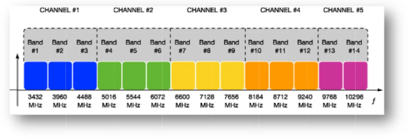
Fig.2-2 shows the plan of the MB-OFDM bands and the channelization within each band. The 14 bands span the range of 3168 MHz to 10560 MHz. In contrast to IEEE 802.11a/g, MB-OFDM employs only QPSK modulation in each sub channel to allow low resolution in the baseband analog-to-digital (A/D) and digital-to-analog (D/A) converters. Usually, bands 1-3 constitute “Mode 1” and are mandatory for operation
wherreas the remmaining bandds are envissioned for hhigh-end prooducts [5]. DS-U cohe desig inher DS-U betw the lo 5.825 wave A fix enab short multi UWB
Figure 2-2 Multi-baand OFDM frequency bband plan
UWB (DSSSS) DS-UWB u rent bandw gn and appl rent frequen UWB syste ween 5.15GH ow band (L 5GHz to 10 uses a comb width. The U ication, say ncy diversit ems is sugg Hz and 5.82 LB) from 3. 0.6GHz. The bination of UWB Forum ys it provide ty and prec gested to av 25GHz. Th 1GHz to 5. e illustration a single-ca m, an indust es low-fadin ision rangin void the in he DS-UWB .15GHz and n is shown i arrier spread try organiza ng, optimal ng capabilit nterference B system ut d the other in Fig.2-3. d-spectrum ation focusi interferenc ties. Recent with narrow tilizes the d is the high design and ing on DS-U e characteri tly, dual-ba w band sys dual band, o band (HB) wide UWB istics, and of stems one is from Unlike con es to transm xed UWB les this sca test possibl ipath envir B devices. nventional mit informat chip rate alable suppo le pulses, onment and wireless sy tion, DS-UW in conjunc ort. By usin DS-UWB d offers pr ystems whic WB transm tion with v ng the wide supports ro ecise spatia ch use narr mits data wit variable-len est possible obust, high al resolutio rowband m th pulses at ngth spread e bandwidth h-data-rate n for locat modulated c t very high ding code w h to produc links in a tion detectio carrier rates. words ce the high on of
Furthermore, DS-UWB provides four key advantages over other wireless technologies: quality of service; high data rates that scale to 1 Gbit/sec or more; lower cost; and longer battery life. That the technology reduces implementation complexity while allows increased scalability, makes it ideal for applications such as high-rate data transmission and power-constrained handheld devices. These attributes mean DS-UWB is well suited to be the physical layer for PANs.
Figure 2-3 DS-UWB operating band (a) low band (b) high band
2.2 Impulse-Radio UWB Communication System
2.2.1 Definition
FCC provides the following definitions for UWB operation [6], and the illustration is shown in Fig.2-4.
(a) UWB bandwidth
The UWB bandwidth is the frequency band bounded by the points that are 10 dB below the highest radiated emission, as based on the complete transmission system including the antenna. The upper boundary is designated fH and the lower
boundary is designated fL.
(b) Center frequency
The center frequency,
f
c, equals (fH + fL)/ 2.The fractional bandwidth equals 2
(
fH − fL)
/(fH + fL).(d) Ultra-wideband (UWB) transmitter
An intentional radiator that, at any point in time, has a fractional bandwidth equal to or greater than 20% or has a UWB bandwidth equal to or greater than 500 MHz, regardless of the fractional bandwidth.
(e) Equivalent isotropically radiated power (EIRP)
The product of the power supplied to the antenna and the antenna gain in a given direction relative to an isotropic antenna. At UWB specification, the signal of 3.1 to 10.6 GHz frequency allocation cannot exceed -41.3dBm/MHz of power spectral density (PSD).
f
Lf
cf
HFigure 2-4 Illustration of UWB
Generally speaking, IR-UWB specification is similar to DS-UWB. The reason is that they both transmit data by pulses. However they still have slight difference in sub-channel allocation. DS-UWB system is divided into high band and low band for avoiding the interference with narrow band communication systems. Therefore, IR-UWB use very short pulses which occupy the almost entire band (3~10 GHz) for
high data rate and average power degradation. In this thesis we focus on IR-UWB and design receiver block circuits suited in IR-UWB system.
2.2.2
Features and Advantages
UWB has a lot of advantages that make it attractive for consumer communications applications [7,8 ]. In particular, IR-UWB systems owns the advantages of
(1) High-data transmission rate
According to channel capacity formula, (i.e. log2(1 ) N
S B
C = × + ), the data capacity
(C) is proportional to channel bandwidth (B). In terms of 7.5 GHz of UWB bandwidth, the transmission rate can reach in 110Mbit/s if the range is less than 10m and up to 480Mbit/s if less than 2m. It is an ideal technology for realizing wireless personal area network (WPAN) systems. In addition, UWB systems coexist with other communication systems band instead of occupying crowded and expansive frequency bands arbitrarily.
(2) Low power consumption
UWB system delivers data by discrete-impulse instead of continuous sinewave, and the hold time of impulse is very short. Compare with continuous-signal of conventional communication system, impulse radio system can achieve ultra low power consumption. The consumption of UWB is only 1/100 of traditional mobile phone, and 1/20 of Bluetooth equipments. Therefore, impulse radio UWB system is superior to typical wireless system concerning battery life and electromagnetic radiation.
(3) Low cost and low complex architecture
Unlike conventional radio system, the UWB transmitter produces a very short time domain pulse, which is able to propagate without the need for an additional RF mixing stage. The signal will propagate well without any additional up-conversion. The reverse
process of down-conversion is also not required in the UWB receiver. In other words, one of the greatest benefits of UWB architecture compared to continuous-wave one is that there is no need for complex circuits such as the power amplifier and frequency synthesizer, and these are the most complex components of conventional architecture. In addition, UWB will have potential of low cost if circuits are integrated in single chip by CMOS process.
(4) High security
Due to the low energy density and the pseudo-random (PR) characteristics of the transmitted signal, the UWB signal is noiselike, which makes unintended detection quite difficult. If the transmitted signal collocates with pseudo-random noise sequence for coding, the receiver must have the accurate transmitter’s pulse sequence. As a result, it can get the right signal from the transmitter, and the impulse radio therefore has high security in data transmission.
(5) High positioning resolution
Due to the characteristic of very narrow impulse, IR-UWB is easy to combine with positioning system and communication system. Moreover, the narrow-impulse has robust penetration, which can apply in precision position in door or below ground. Compared to general global position system (GPS) mechanism which only works in visible range of the positioning satellite, impulse radio can achieve an accurate scale of centimeter.
(6) Multi-path capacity
The radio signal of the conventional wireless communication mostly adopts continuous-wave, and the sustained time is far longer than multi-path propagation time. So multipath effect limits the quality of service and data rate and causes channel distortion. Besides, traditional receivers deal with multi-path signal by rake receivers. When multipath effect becomes more serious, the circuits’ complexity, power, and
storage requirements are potentially higher. However, the emission of impulse-radio UWB is narrow impulse, which can directly be decomposed in multipath without interference. It is suitable in multi-path signal processing.
2.3 Pulse Shaping
In impulse-radio UWB, it delivers data by very short pulses. Different kinds of pulse would affect the spectrum distribution [9]. In this section we will introduce some pulses and each spectrum used in UWB system.
(1) Gaussian pulse
As shown in Fig.2-5, Gaussian pulse is the common waveform in impulse communication. The mathematic equation is
2
[( ) / ]
( )
t Tc Tauw t
=
Ae
− − (2-1) where A is amplitude, is the pulse width, and is the parameter about pulse forming, or called pulse shape parameter, which is mainly in the adjustment of central frequency and bandwidth of signal. This spectrum allocation has large DC component and the central frequency is close to low band.c
T Tau
Figure 2-5 Gaussian pulse and spectrum allocation
(2) Gaussian monocycle
pulse. It can be observed that the central frequency moves toward higher band. However, it still cannot satisfy the spectrum mask of UWB. The mathematic equation is
2 2 [( )/ ]
( ) 2
A
(
)
t Tc Tauw t
e t Tc e
Tau
− × −= ×
× × − ×
(2-2)Figure 2-6 Gaussian monocycle and spectrum allocation
(3) Scholtz’s monocycle
As shown in Fig.2-7, the waveform was presented initially in [10] by Dr. Scholtz. This pulse approximates the 2nd derivative form of Gaussian pulse, and the mathematic equation is 2 2 ( ) 2
( )
[1 4 (
) ]
au t Tc T aut Tc
w t
A
e
T
ππ
− −−
=
−
(2-3)We can observe the spectrums of these three kinds of pulse above. Gaussian pulse has more DC components, which would degrade the efficiency of antenna radiation. The 2nd derivative of Gaussian pulse (or Scholtz’s monocycle) has wider 3dB bandwidth and fewer components in low band. This pulse occupies much bandwidth under UWB specific mask and be appropriate in the waveform of impulse radio UWB.
Figure 2-7 Scholtz’s monocycle and spectrum allocation
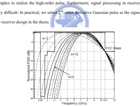
(4) Higher-order derivatives of Gaussian pulse
Higher-order derivatives of Gaussian pulse indicate that the derivative order is higher than three. Although more derivative orders cause the central frequency toward high frequency [11], as shown in Fig.2-8, but the circuit architecture becomes more complex to realize the high-order pulse. Furthermore, signal processing in receiver is very difficult. In practical, we select 2nd-order derivative Gaussian pulse as the signal of the receiver design in the thesis.
2.4 Pulse Modulation
Information can be encoded in a UWB signal in a variety of methods. The most popular modulation schemes developed to date for UWB are pulse-position modulation (PPM), on-off keying (OOK), pulse-amplitude modulation (PAM) and binary phase-shift keying (BPSK), which also is called biphase. Other schemes have been selected by various groups to meet the different design parameters for different applications. We will make a brief explanation in each modulation method as follows. PAM (or OOK)
PAM is based on the principle of encoding information with the amplitude of the impulses, as shown in Fig.2-9. The picture shows a two-level modulation, respectively. The difference is that bit 0 is presented by zero and lower amplitude, where one bit is encoded in one impulse. As with pulse position, more amplitude levels can be used to encode more than one bit per symbol.
Figure 2-9 (a) OOK (b) PAM
BPSK (Biphase)
In biphase modulation, information is encoded with the polarity of the impulses, as shown in Fig.2-10. The polarity of the impulses is switched to encode a 0 or a 1. In this
case, only one bit per impulse can be encoded because there are only two polarities available to choose from.
Figure 2-10 BPSK
PPM
PPM is based on the principle of encoding information with two or more positions in time, referred to the nominal pulse position, as shown in Fig.2-11. A pulse transmitted at the nominal position represents a 0, and a pulse transmitted after the nominal position represents a 1. The picture shows a two-position modulation, where one bit is encoded in one impulse. Additional positions can be used to provide more bits per symbol. The time delay between positions is typically a fraction of a nanosecond, while the time between nominal positions is typically much longer to avoid interference between impulses.
Figure 2-11 PPM
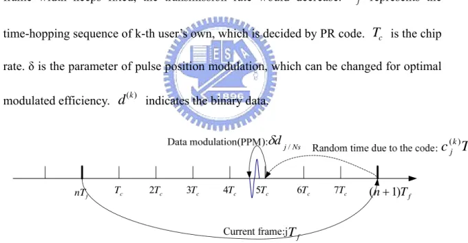
Additionally, combining with PPM and random-time hopping code can flat the spectrum of signals. It also mitigates multi-path effect and interference between clients. As a result, it accomplishes UWB time-hopping system for multiple-user case. The
transmitted signal for single user is coding by pseudo random code (PR code) to control the pulse position in each frame. The equation of time-hopping PPM can be presented as [7] ( )
(
)
( ) ( ) ( ) ( ) ( ) /(
)
s k k k k k tr tr f j c j N jS
t
w
t
jT
c T
δ
d
∞ =−∞=
∑
−
−
−
(2-1)where ( )k ( ( )k is the transmitted signal of k-th user, is the transmitted pulse,
tr
S t )
w
trf
T is pulse repetition time, which also be called time frame width. For fixed Tf ,
symbol rate (
R
s) can be represented as Rs =1/N Ts f . It can be observed that if time frame width keeps fixed, the transmission rate would decrease.c
( )jk represents the time-hopping sequence of k-th user’s own, which is decided by PR code. is the chip rate. δ is the parameter of pulse position modulation, which can be changed for optimal modulated efficiency. indicates the binary data.c
T
( )kd
f nT Tc 2Tc 3Tc 4Tc 5Tc 6Tc 7Tc (n+1)Tf f T Ns j d /δ
c k jT
c
( )Figure 2-12 Graphic form of time-hopping pulse position modulation
2.5 IR-UWB Receiver
The main characteristic of UWB impulse radios is that very low emission power density can be achieved by spreading the energy of short-time pulses in wideband. These radios present the advantage of not requiring up/down conversion of frequency,
which results in reduced complexity and low cost of manufacturing. According to the demodulated method, IR-UWB receivers can be divided into two architectures: coherent receiver and non-coherent receiver. Coherent receivers, as shown in Fig.2-13, rely on the correlation of the received pulses and a local template demand complex implementations [12,13]. Because of short pulse adoption and known position, it has some advantages of high data rate and high SNR. Unfortunately, it needs precision timing synchronization between transmitter and receiver ends. Generally the requirement is realized by delay lock loop (DLL) circuits to achieve synchronization. On the other hand, the non-coherent receiver shown as Fig.2-14 requires neither pulse synchronization nor estimation of the shape of the incoming pulses. Instead, it recovers the energy of the pulses during a symbol time and compares it to the noise level in order to determine the presence or absence of a symbol [14]. The main drawback of using this kind of detector is that the UWB pulses cannot be detected when the signal-to noise ratio (SNR) is very low, and hence, it cannot make use of the processing gain that spread spectrum systems have. Accordingly, the non-coherent impulse receiver will only work properly when the SNR is above a threshold which is close to the noise level. Due to the very limited power that is allowed in the UWB transmitter, this only occurs at very short distances.
As to sensitivity, the BER vs. SNR curves of a non-coherent receiver is simulated and compared to that of a coherent receiver using BPSK modulation [14]. The simulation results are presented in Fig.2-15. Both simulations are executed for 10, 25, 50, and 100 Mbps using a pulse rate of 100MHz. The monocycles pulses are shaped to use the low part of the UWB spectrum 3.1GHz-5GHz. As expected, the coherent receiver presents processing gain and hence requires less SNR than the non-coherent receiver for a fixed BER. In addition, the simulation shows that the non-coherent receiver can still detect the UWB pulses for SNR close 0 dB.
Figure 2-13 Architecture of the coherent receiver
Figure 2-14 Architecture of the non-coherent receiver
Figure 2-15 Performance curves of a non-coherent receiver and a coherent receiver using BPSK modulation
Chapter 3
Design of the Ultra-wideband LNA and Correlator
3.1 Overview
In this chapter we propose two circuits, which can apply in the front-end receiver of impulse-radio UWB system. The first one is a UWB LNA with transformer-feedback matching network. It employs the characteristic of the transformer to achieve good input matching and noise performance. Subsequently, the correlator with dynamic gain control has presented. In addition, the wide bandwidth is achieved by canceling the dominant pole at the internal node with the zero introduced by the shunt inductor at the loading stage. These circuits have been fabricated by TSMC 0.18μm 1P6M CMOS technology. We also exhibit the simulation and measurement results of each circuit.
3.2 A UWB LNA with Transformer Feedback Matching Network
In this section we propose another UWB LNA design method. It utilizes transformer feedback for wideband matching and noise degradation. First, the general monolithic transformer prototype is introduced. Then we analysis different kinds of transformer and list each advantages and disadvantages. Then we demonstrate that the design concepts in the proposed UWB LNA in detail. Subsequently, we show the simulation and measured results. Finally, the differences between the simulation and measured results are discussed.
3.2.1 Introduction of Monolithic Transformers
Transformers have been used in radio frequency (RF) circuits since the early days of telegraphy. Recent works have shown that it is possible to integrate passive
transformers in silicon IC technologies because of useful performance characteristics [15,16,17]. In general, the operation of a passive transformer is based upon the mutual inductance between two conductors. Basically, the transformers are used for the following three different functions.
1. Impedance matching: depending on the number of windings, the transformer has the property to change the impedance of the primary or secondary when measuring from the opposite port.
2. Balun: balanced to unbalanced conversion and vice versa
3. DC isolation: obtained with the magnetic (nonelectric) connection between the primary and secondary
Fig.3-1(a) summarizes the basis of an ideal transformer where the primary self-inductance and the secondary self-inductance are characterized with ideal inductors. The mutual inductance is represented by
1
L L2
M , the primary and secondary
currents and voltages are , , , and , and the primary and secondary winding numbers are and , respectively. The coupling factor k is defined by
1
i i2 v1 v2
1
N N2 M , ,
and and represents the energy transmitted from the primary port to the secondary port [18,19].
1 L 2
L
The behavior of the ideal transformer in Fig.3-1(a) is ruled by its characteristic equations 1 1 2 2
v
j L
M
i
v
M
j L
ω
ω
⎡ ⎤ ⎡
⎤ ⎡ ⎤
=
⎢ ⎥ ⎢
⎥ ⎢ ⎥
⎣ ⎦ ⎣
⎦ ⎣ ⎦
(3-1) 1 2i
1 2 1 2 1 2v
i
N
n
v
=
i
=
N
=
(3-2) 1 21
M
k
L L
=
≤
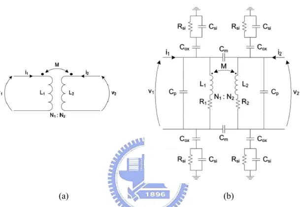
(3-3)because of substrate loss and parasitic effects. Thus, the electrical model of an integrated transformer must be redefined, and the equivalent model of an integrated transformer is shown in Fig.3-1(b).
(a) (b)
Figure 3-1 (a) Electrical model for an ideal transformer (b) Equivalent circuit of an integrated transformer
where and represent the ohmic losses due to the resistivity of the inductor metal tracks; is the capacitive coupling caused by the voltage difference between the turns in the same metal, which form a spiral; represents the capacitive coupling caused by the voltage difference between the turns of the primary and secondary spirals; is the capacitive coupling between the metal used for each inductor and ground;
1 R R2 p C m C ox C si
(a) (b)
(c) (d)
Figure 3-2 Monolithic transformer winding configurations (a) Parallel conductor winding (b) Interwound winding (c) Overlay winding (d) Concentric spiral winding
A monolithic transformer is constructed using conductors interwound in the same plane or overlaid as stacked metal layers, as shown in Fig.3-2(a). The type of parallel conductor winding is interwound to promote edge coupling of the magnetic field between windings. The primary and secondary windings lie in the same plane, as illustrated in the cross-section at the right of Fig.3-2(a). Because of the asymmetric characteristic, the ratio of transformer turns is not unity.
As shown in Fig.3-2(b), the type of interwound winding has feature of symmetry. It ensures that electrical characteristics of primary and secondary are identical when they have the same number of turns. Another advantage of this design is that the transformer terminals are on the opposite sides of the physical layout, which facilitates connections to other circuits.
Integrated transformers with multiple conductor layers are illustrated in Fig.3-2(c). The overlay winding utilizes both edge and broadside magnetic coupling to reduce the
overall area required in the physical layout. Flux linkages between the conductor layers can be improved as the intermetal dielectric is thinned. In addition, there is a large parallel-plate component to the capacitance between windings due to the overlapping of metal layers, which limits the frequency response.
Transformers can also be implemented using concentrically wound planer spirals as shown in Fig.3-2(d). The periphery between the two windings is limited to just a single turn. Therefore, mutual coupling between adjacent conductors contributes mainly to the self-inductance of each winding and not to mutual inductance between the windings. As a result, the concentric spiral transformer has less mutual inductance and more self-inductance than other types. This kind of low ratio of mutual inductance to self-inductance is useful in applications such as high-performance broadband amplifiers. The four kinds of monolithic transformers above are summarized in Table 3-1. We can select an appropriate type for an specific design. For instance, when designing an amplifier for UWB, we can use the type of concentric spiral winding for achieving wideband response.
Table 3-1 Comparison of differential transformers Transformer type Coupling coefficient
Self
L fSR
Parallel conductor winding Middle Low High
Interwound winding Middle Low High
Overlay winding High High Low
3.2.2 Design Concepts
Figure 3-3 Schematic of the proposed UWB LNA.
Transformer-feedback matching network
The proposed LNA is shown in Fig.3-3. The transformer consists of two inductors. The primary winding is shunt with the gate end of M1; the secondary winding is series to the source end of M1. There are no extra lumped elements placing at the input port excluding ac-coupling capacitance and bypass capacitance . In general, the common-source amplifier with the inductive degeneration has been popularly used because it can generate real impedance to match source resistance. The imaginary part can be cancelled by the reactive elements located at the gate of M1. But the method only suits in narrow band amplifier design because it satisfies above only at a specific frequency. Therefore, we modify the conventional matching skills for broadband matching purpose as explained in the following. The simplified input impedance diagram is shown in Fig.3-4.
1 D
Ls T
ω
1 gs C P L S L rSZ
inFigure 3-4 The simplified input impedance network
s
r is the parasitic resistance of and the parasitic resistance of is neglected for
simplifying the analysis. is the gate-source capacitance of M1. The input impedance can be represented in s-domain as
s L Lp 1 gs C 1 1 1 2 1 2 1
( ) (
)
(
1/
) //
(1
)
(
)
1
(
)
in s S S gs P gs P S gs s T S gs S Pgm
Z
s
r
L
sL
sC
sL
C
sL
s L C
r
L
s C
L
L
ω
⎡
⎤
=
+
+
⎣
+
⎦
+
=
+
+
+
+
(3-4)The imaginary part forms a equation comprising three zero-point frequencies, one resonant frequency is zero, the others are both 1/ LSCgs1 . It means that if the
operating frequency is equivalent to 1/ LSCgs1 , the impedance matching can
accomplish due to the cancellation of the imaginary part. Generally is a fixed value as long as the biasing is determined. Then, would need to be decreased as the operating frequency rises in order to meet the matching condition. This is the reason that we use transformer in the matching network. The self-inductance and mutual inductance of the transformer are appropriately selected and the practical inductance looked into the source of M1 decreases apparently. The broadband matching can be realized by the phenomenon of the transformer feedback.
1
gs
C
s
Noise Analysis and Current-reuse Technique
The noise performance of the proposed topology is determined by two main contributors: the losses of the input network and the noise of the first amplifying device (M1). The general expression for noise figure as given by a classical noise theory [20]:
2 min n s s opt, s
R
F
F
Y
Y
G
=
+
−
(3-5)where is the minimum noise factor, is the noise resistance, is the source admittance ( ), is the optimum source admittance ( ), and is the real part of the source admittance. We can derive the optimal noise figure if the condition of min F Rn Ys opt = s s Z Y =1/ s Z opt s Y, opt opt s s Z Y, 1/ , s G Z ≈ is sustained.
In order to have adequate power gain at the condition of the limited power consumption, we adopt the current-reuse technique at gain stages. The second stage ( ) is stacked on the top of the first stage ( ). A coupling capacitor ( ) and a bypass capacitor ( ) are required for this topology. Both and are metal-insulator-metal (MIM) capacitors. The choice of large capacitance of is preferred to perform better signal coupling. However, too large MIM capacitors may suffer from parasitic capacitance between the bottom plate of the capacitor and ground, which would degrade the circuit gain. The value of is chosen to be as large as possible to provide ideal ac ground. In addition, and are designed to have a peaking characteristic to compensate the low frequency roll-off of the device.
2 M M1 CD2 C 2 b C CD2 b2 D C 2 2 b C L R LL B
L connects between the main stage and buffer in order to enhance wideband
characteristic. The further bandwidth extension is achieved due to a series LC resonance with the gate capacitance of . Various values of can cause different performances of bandwidth enhancement. Fig.3-5 exhibits the gain performance with different value of . We select =2.75 nH for the trade-off between bandwidth and
4 M B L B L B L
gain flatness for our design purpose. 0 2 4 6 8 10 12 14 16 Frequency (GHz) -30 -20 -10 0 10 20 30 G a in ( d B ) L=2.02nH L=2.38nH L=2.75nH L=3.13nH L=3.52nH L=3.92nH
Figure 3-5 Gain performance with LB variation
A source follower is adopted as the output buffer for a wideband output matching purpose. The current source is different from the conventional one because it is driven by itself without extra bias voltage. The buffer is not needed if the LNA integrates directionally to mixer or other circuit block.
Layout consideration
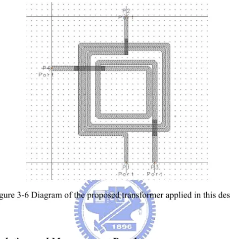
The geometric layout of the transformer [19] will impact the input return loss, noise figure, and stability, etc. Rectangular-type and concentric spiral windings are adopted to reduce the Q factor for wideband applications. Turn numbers of separate inductor and the spacing between the two inductors inside the transformer are appropriately chosen to achieve feasible self-inductance and mutual inductance, respectively. The transformer of this proposed LNA is simulated by ADS Momentum and the geometric photo is shown in Fig.3-6. Metal 6 is used to layout the transformer because that thicker metal reduces the ohmic losses in the primary and secondary windings of a planar transformer. The size of M1 is 150×0.18 μm2 for noise optimum
source impedance. The 130×0.18 μm2
of size is selected as the trade-off between gain and nonlinearity. The value of is 4.8nH to make sure in inter-stage stability.
2 M
int
L
Figure 3-6 Diagram of the proposed transformer applied in this design
3.2.3 Simulation and Measurement Results
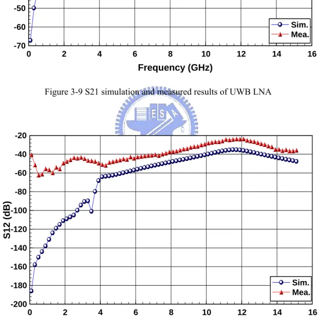
The Ultra-wideband LNA with the transformer feedback matching network is fabricated using TSMC 0.18μm RF CMOS process. Fig.3-7 shows the microphotograph and the total area is about 0.6 mm2. The whole measurement is on-wafer test on the RF probestation. Two three-pin GSG RF probes are used for transmission of input and output signal, and one three-pin PGP DC probe provides the biasing and supply voltage. The scattering parameters are measured by HP 8510C. Fig.3-8~3-11 illustrate the measured results of individual s-parameters. The simulation results are also put together to compare the difference. In Fig.3-8 the measured input return loss (S11) is better than -9.8 dB over the entire UWB band with two dips at 3.7GHz and 6.2GHz. The performance proves that transformer feedback is feasible in wideband matching. The output return loss (S22) is -10.4 dB below from Fig.3-11. Fig.3-10 shows that the
measured isolation form output to input is under -28 dB. Fig. 3-9 is the simulated and measured results of the power gain. The measured power gain has a peak value in 12.4dB and the average value is 11.2dB with 1.2dB ripple from 3.1GHz to 10.6GHz. The result presents a good feature of flatness. For the noise figure measurement, we exploit noise figure analyzer (Agilent N8975A) and noise source (Agilent 346C). The results of simulated and measured noise figure are shown in Fig.3-12. It is obvious that the curves of and are mostly overlap in the UWB band. It indicates that transformer feedback has an optimal noise figure performance as well. The measured results of NF have the minimum value 3.2dB at 5GHz and the average is 4dB.
sim
NF NFmin
As to in-band linearity, the 1-dB compression input point ( ) with 5GHz is -14dBm as shown in Fig.3-13. Two-tone signals of 5GHz and 5.01GHz are applied to the LNA to observe the input referred third-order intercept point (IIP3), and the spectral diagram has shown in Fig. 3-14. The measured value is in the range of -5 to -10dBm over 3 to 10-GHz system while is about -22dBm to -14dBm. From Fig.3-15 it can observed that IIP3 is around 10 dB less than over the entire band.
dB P1 dB P1 dB P1
Table 3-2 makes a comparison between simulation and measurement results. It demonstrates that they are only slightly different. Table 3-3 lists some previously-proposed references. Each input matching method and characteristic of LNA is summarized to make comparison. It can be observed that our UWB LNA with transformer feedback has competitive performances at I/O return loss, power gain, power consumption, and even chip size.
Figure 3-7 Microphotograph of the proposed LNA 0 2 4 6 8 10 12 14 16 Frequency (GHz) -30 -25 -20 -15 -10 -5 0 S 1 1 ( d B ) Sim. Mea.
0 2 4 6 8 10 12 14 16 Frequency (GHz) -70 -60 -50 -40 -30 -20 -10 0 10 20 S 21 (d B ) Sim. Mea.
Figure 3-9 S21 simulation and measured results of UWB LNA
0 2 4 6 8 10 12 14 16 Frequency (GHz) -200 -180 -160 -140 -120 -100 -80 -60 -40 -20 S 12 (d B ) Sim. Mea.
0 2 4 6 8 10 12 14 16 Frequency (GHz) -16 -14 -12 -10 -8 -6 -4 -2 0 S 22 (d B ) Sim. Mea.
Figure 3-11 S22 simulation and measured results of UWB LNA
2 4 6 8 10 12 14 Frequency(GHz) 0 2 4 6 8 10 12 N o is e F ig u re ( d B ) NFmin NFsim NFmea
Figure 3-13 Measured input 1dB compression point at 5GHz
Figure 3-14 Spectral diagram of the IIP3 measurement (one tone is 5GHz, and the other tone is 5.01GHz)
3 4 5 6 7 8 9 10 Frequency (GHz) -22 -20 -18 -16 -14 -12 -10 -8 -6 -4 P1dB(dBm) IIP3(dBm)
Figure 3-15 Measured P1dB and IIP3 curves over the UWB band
Table 3-2 Comparison of simulation and measurement results of UWB LNA Simulation results Measurement results
S11 (dB) <-10.7 <-9.8 S21 (dB) 12 11.2±1.2 S12 (dB) <-36 <-24 S22 (dB) <-11.6 <-10.4 NF (dB) <4.6 3.2~5.5 P1dB (dBm) -14 ~ -23 -14 ~ -22 IIP3 (dBm) -3 ~ -13 -5 ~ -10 Power dissipation (mW) 11.4 11.1
Table 3-3 Performance of summary and comparison to other wideband LNAs Ref. BW (GHz) Input matching method S11 (dB) S21 (dB) NF (dB) IIP3 (dBm) Power (mW) Technology Area ( 2) mm [21] 2.3~9.2 3rd-order Chebyshev filter <-9.9 9.3 4~9.2 -8.2~-5.6 9* @1.8V 0.18um CMOS 1.1 [22] 3.1~10.6 Distributed amplifier <-10 16.8~19.2 5~7 N/A 54 @1.8V 0.18um CMOS 2.2 [23] 3~5 Resistive-shunt feedback <-9 9.8 2.3~5.2 -7 12.6 @ 1.8V 0.18um CMOS 0.9 [16] 3.1~10.6 Dual feedback <-11.2 10.8~12 4.7~5.6 -12 ~-10.6 10.57* @1.5V 0.18um CMOS 0.665 This work 3.1~10.6 Transformer feedback <-9.8 11.2±1.2 3.2~5.5 -10 ~ -5 11.1 @1.5V 0.18um CMOS 0.6
* without adding consumption of buffer stage
3.2.4 Discussion
In section 3.2, we propose a novel UWB LNA and implement successfully by TSMC 0.18μm CMOS process. This circuit uses the transformer feedback topology to realize broadband matching and noise optimization. At the gain stage, it adopts current-reuse technique to have adequate gain performance under power consumption limits. A source follower with self-biasing can reduce extra bias voltage and achieve output matching. The measured results of S11, S21, and S22 are similar to the simulation results. The measured NF is close to simulation result at the low band and only higher than simulation result about 1dB at the high band. The reason may be that parasitic resistance affects apparently at the higher frequency band. As to linearity, the maximum IIP3 is -5dBm at 6GHz while is -14dBm. It can be observed that our UWB LNA with transformer feedback has competitive performances at I/O return loss, power gain, power consumption, and even chip area.
dB
3.3 Analog Correlator with Dynamic Gain Control
This section describes the circuit design principle of a correlator suitable for UWB systems. The technique of dynamic gain control is inserted for a VGA-like architecture in this correlator. The simulation and measurement results are exhibited and discussed in the final of this section.
3.3.1 Design Concepts
The function of correlator is detecting and demodulating the received signal for the following A/D converter or comparator. Normally a correlator incorporates a separate multiplier and a separate integrator. There are some main problems in designing the correlator of pulse-based UWB receiver [24]. For instance, the multiplier should have very wide-band input frequency response, even the lower band UWB pulse is very large depending on data and applications. Therefore, though the DC offset current or 1/f noise current must be much smaller than the signal current, it can integrate on the integral capacitor for a much longer time the multiplied signal. Another problem is that after the pulse correlation, the output voltage should maintain for a long time for the ADC to sample, but the output impedance of the integrator normally is not large enough, and results in large leakage from the integrator. These ultra-wideband characteristics of the input pulses make the digital domain correlation not suitable in this application. According to above discussions, we adopt the analog correlator in UWB system receiver.
Generally multipliers are much more difficult to design than mixers. For mixers, the gain doesn’t need to vary linearly with the LO signal, and only the first harmonics of the LO is needed to multiply with the input signal. Working in linear region makes the multiplier very difficult to bias. In this design of multiplier we apply a Gilbert-cell with bandwidth extension and linear adjustment for UWB systems.
Figure 3-16 A Gilbert multiplier
Gilbert-cell multiplier is the common architecture used in communication circuit [7]. Besides circuit simplicity and high isolation, double-balanced type also has some advantages about eliminating even-mode harmonic and common-mode noise. For example in Fig.3-16, the output differential current can be expressed as follow
7 8 3 5 4 6 3 4 6 5
(
) (
(
) (
)
out D D D D D D D D D D)
I
I
I
I
I
I
I
I
I
I
I
=
−
=
+
−
+
=
−
+
−
(3-6)=
−
+
−
−
−
=
kV
ISS
k
V
V
ISS
k
V
V
kV V
X Y Y Y Y X Y[ (
)
(
) ]
2 2 2 22
2
2
2
2
(3-7)Based on the Gilbert-cell, we design a novel correlator with dynamic gain control, whose overall schematic of circuit is shown in Fig.3-17. The additional transistors (M ,C1
2
C
M ) are added at the source of the transconductance stage. The additional transistors
operating in triode region are used as resistors and each resistance value is 1 ( ) ds r = n ox G S TH W C V V L
μ − . The resistance looking in current source is . From Fig.4-18 we can know that the overall resistance looking in the source of
o
r
1 M is
//
s o ds ds
R
=
r
r
≈
r
, and the overall transconductance is Gm=gm/1+gmRs, whereis the intrinsic transconductance of
gm M1 . It means that is dominantly
controlled by . Moreover, the value of can be changed by . Thereby a tunability is achieved by changing the value of the control voltage at the gate of transistor Gm ctrl V ds
r
c dsr
M . By adjusting the magnitude of transconductance, the amplitude of output
waveforms can be controlled.
d s
r
o
r
Figure 3-18 The transconductance stage with source degeneration
As for loading end, the correlator needs wider frequency response for UWB systems. The zero-point frequency is generated purposely to cancel the dominant pole frequency for achieving wideband characteristic. There are four transistors connecting at the load-end of the first stage, so the parasitic capacitance is large enough to form the dominant pole. The PMOS (ML1,ML2) with diode connecting plays the role of the load
resistors whose value are R =
gm ro
1
/ / . There are two extra advantages about diode-connected PMOS as load. First, the cross voltage is Vov +Vth, which can make
sure the next stage at the on state. Second, the correlator can be viewed as a direct conversion architecture. The interference of the flicker noise of NMOS affects the received signal deeply. For the reason, PMOS is used at the loading stage due to the lower flicker noise than NMOS.
The function of integration is to spread the multiplied signal and hold for a long time for the next stage. Generally some references apply Gm-C-OTA integrator in UWB systems [12,13]. The benefits are low voltage variation and unapparent parasitic capacitance effect, which can stabilize the integration. In order to have faster integration and shorter rise time, this architecture must need large current to drive. Besides, another parallel transconductance is used to create a feed-forward path for compensating the high-frequency response and building the rapidly rising edge of the output signal. This
architecture is good but it cost large power because of multi-stage circuits. In this design we directly add a capacitor ( ) at the differential output of the multiplier. Because ofC1
o u t o u t
d V
I C
d t
= and Vout = 1 Ioutdt
C
∫
, the integration results can be achieved atthe differential output of the multiplier. The method not only reduces complexity of the circuit design but also avoids extra power dissipation of separate integrators.
It can be observed that the signal after integrating operation still has apparent drop and don’t hold for a long time. Two-stage architecture is proposed in this correlator because that the second stage can amplify and integrate signal again. The mechanism is also presented in Fig.3-17. is the second integrating capacitor and locates between the differential output of the second stage. Moreover, there is a switch parallel to . The purpose of the switch is resetting the output data by controlling voltage . When the switch turns off, the circuit works normally; when the switch turns on, the differential output is short. Voltage is a square pulse train with 1.8V amplitude. The period of is similar to input data and the duty cycle is 50%.
2 C 2 C rst V rst V rst V (a) (b)
Finally, in order to measure the output waveform, source followers are added at the final stage for 50Ω matching (not illustrate in Fig.3-17). Unfortunately, it may generate unnecessary parasitic capacitance and degrade performance. The buffer is not needed if the correlator integrates directly to other circuits.
3.3.2 Simulation and Measurement Results
Fig.3-20 illustrates that the input signal is an ideal Gaussian monocycle, which amplitude is ±0.4V. In simulation verification the pulse repetition rate is 100MHz. The reason is for the sake of verifying the feasibility of the correlator in high data rate. The simulation output waveform is shown in Fig.3-21. In the thesis we list the definitions about rise time, fall time, and hold time. The time required for a signal to change from a specified low value to a specified high value is rise time. Typically, these values are 10% and 90% of the peak value. Corresponsively, fall time is the value of 90% and 10% of the height. Hold time is the duration when the amplitude of signal is over 90% of the peak value. It can be observed that the rise time, fall time, and hold time are 1.3ns, 3.0ns, and 1.1ns, respectively in Fig.3-21. Different output waveforms with variation are shown in Fig.3-22. The range of output amplitude is 0.08V to 0.131V while is 0.7V to 1.8V. The output amplitude is not proportional to because of nonlinear characteristics of transistor. As to linearity, the linear input range is from -0.17V to +0.17V and has been shown in Fig.3-23. A good linearity is obtained as well.
ctrl V ctrl V ctrl V
The practical input signal is a Gaussian monocycle generator implemented by schottky diodes and lumped elements on the PCB. The generator is for the purpose to converts square waves to Gaussian monocycles. The photo and waveform is shown in Fig.3-24. As for the measurement setup, the chip on the PCB by wire bonding is adopted because of limits of probes. The measured results of singly-ended output waveforms are shown in Fig.3-26, 3-27. In Fig.3-26, the peak value is 44.5mV and rise
time is close to 1.8ns while repetition data rate and are 100MHz and 1.8V, respectively. Fig.3-27 shows that the peak value is 18.1mV while is 0.7V. Fig.3-28 records the different differential output amplitude versus the control voltage ranging from 0.7V to 1.8V. It can be observed that the trend is similar to simulation. Fig.3-29 shows the chip microphotograph of correlator.
ctrl
V
ctrl
V
Figure 3-20 Input waveforms
(a) (b)
Figure 3-22 Simulation (a) different output waveforms with variation (V =0.7V~1.8V) (b) output amplitude versus
ctrl
V
ctrl
ctrl
V
Figure 3-23 Simulation output amplitude versus input amplitude
(a) (b)
Figure 3-25 Photo of chip on board with bonding wire