國 立 交 通 大 學
電子工程學系 電子研究所
碩 士 論 文
應用於非極性氮化鎵發光二極體元件以改善光
萃取效率的極性選擇化學蝕刻
Integration of Nonpolar A-Plane Gallium
Nitride Fabricating and Chemical Etching
Processes for Lighting Efficiency Enhancement
of Light-Emitting Diodes
研 究 生 : 莊 凱 麟
指導教授 : 張 俊 彥 院士
應用於非極性氮化鎵發光二極體元件以改善光
萃取效率的極性選擇化學蝕刻
Integration of Nonpolar A-Plane Gallium
Nitride Fabricating and Chemical Etching
Processes for Lighting Efficiency Enhancement of
Light-Emitting Diodes
研 究 生: 莊 凱 麟
Student:
Kai-Lin
Chuang
指導教授: 張 俊 彥 院士 Advisor: Prof. Chun-Yen Chang
國 立 交 通 大 學
電 子 工 程 學 系 電 子 研 究 所
碩 士 論 文
A Thesis
Submitted to Department of Electronics Engineering and
Institute of Electronics
College of Electrical and Computer Engineering
National Chiao Tung University
In Partial Fulfillment of the Requirements
For the Degree of Master
In
Electronics Engineering
July 2010
Hsinchu, Taiwan, Republic of China
應用於非極性氮化鎵發光二極體元件以改善光
萃取效率的極性選擇化學蝕刻
學生:莊凱麟 指導教授:張俊彥 院士
國立交通大學 電子工程學系 電子研究所 碩士班
摘
要
半導體發光二極體具有成為新世代高發光效率固態照明的特定必須條件,包 含可調變發光頻譜以及材料磊晶特質…等等,其中三族氮化物可以磊晶形成具有 藍光或紫外發光波段的多重量子井結構,而這正式實現白光固態照明所必需的光 源。然而依據現有磊晶以及元件製程技術,依舊無法克服三族氮化物材料特性— 非對稱晶體結構—所引發的特殊效應:量子侷限史塔克效應。此效應導致極性面 三族氮化物材料中的電子電洞分佈機率最大值錯位,意即導電帶與價帶傾斜,使 得電子電洞複合發光機率大幅下降,並間接導致低水平的「內部量子效益」。此 外,如何有效將電子電洞複合產生的光子萃取出元件結構外,以直接對「照明」 做出貢獻是另一項課題,因為此「光萃取效率」所影響的是「外部量子效益」, 或者可通稱為半導體發光二極體的「發光效益」。 本篇論文包含了如何在溝渠圖形化的 m 面藍寶石基板上、溝渠圖形化的無 極性a 面氮化鎵模板上(磊晶於 γ 面藍寶石基板上)利用有機金屬化學氣相沉積方 法磊晶出高結晶品質的無極性 a 面氮化鎵。利用在溝渠圖形化的 m 面藍寶石基 板上成長高結晶品質無極性a 面氮化鎵所得到的磊晶經驗,並將之應用到溝渠圖 形化的無極性a 面氮化鎵模板上,使用「溝渠圖形化側向磊晶成長方式」,可以得到高結晶品質、平坦的無極性a 面氮化鎵於 γ 面藍寶石基板上。在這一高品質 的無極性 a 面氮化鎵基板上,無極性氮化銦鎵/氮化鎵多重量子井結構可以成功 實現,並具有藍光440nm 的發光波段。 此一有機金屬化學氣相沉積方法所依賴的實驗關鍵在於較低的五族/三族原 子比例,其值大約100。而成長模式主要依靠正 c 方向的快速成長面以達到側向 完全癒合平坦的目標。使用「溝渠圖形化側向磊晶成長方式」所得到的高結晶品 質、平坦的無極性a 面氮化鎵,其差排密度可由初始 γ 面藍寶石基板上的 a 面氮 化鎵的 1×1010cm-2大幅降低到在側向成長區域的 1×108cm-2。本論文中並針對利 用此兩種方式:「溝渠圖形化的m 面藍寶石基板上磊晶」、「溝渠圖形化的無極性 a 面氮化鎵模板上磊晶」所得到的高結晶品質無極性 a 面氮化鎵進行分析,並搭 配掃描式電子顯微鏡、穿透式電子顯微鏡進一步針對缺陷分布以及形成原因進行 探究。 由於使用「溝渠圖形化側向磊晶成長方式」所得到的高結晶品質、平坦的無 極性a 面氮化鎵其存在特殊的孔洞於氮化鎵/γ 面藍寶石基板介面,因此本文中利 用氫氧化鉀溶液針對這些因溝渠圖形化設計以及磊晶限制所留下的孔洞進行蝕 刻處理。蝕刻處理所選定的試片包含了完整磊晶的無極性氮化銦鎵/氮化鎵多重 量子井結構,以針對蝕刻分析是否對發光性質造成影響。氫氧化鉀溶液蝕刻條件 控制在100°C、120°C、140°C;濃度條件維持在 5 wt. %、10 wt. %以及 20 wt. %; 蝕刻時間則選擇10min、20min、40min、80min 以及 160min。藉由調整不同條件 組合的蝕刻條件發現在低溫低濃度的狀況下,氫氧化鉀溶液對於存在高結晶品 質、平坦的無極性a 面氮化鎵/γ 面藍寶石基板介面的孔洞無顯著的蝕刻效果,蝕 刻速率約為 2.35±1.67nm/min,速率慢且蝕刻差異大;高溫高濃度的狀況下則可 以得到有效的蝕刻效果,蝕刻速率約為 26.0±1.90nm/min,速率雖快但蝕刻差異 大。而中間溫度120°C 以及 10 wt. %的組合提供了 13.6±0.90nm/min 的蝕刻速率,
具有可接受的蝕刻速率且蝕刻差異降低到1nm/min 以下。 此一蝕刻方式可以將存在高結晶品質、平坦的無極性a 面氮化鎵/γ 面藍寶石 基板介面的孔洞蝕刻成由{11-22}面以及+c 面所構成的等腰三角形、梯形或者因 缺陷導致的混合形。這些蝕刻行為可歸類為「極性選擇蝕刻行為」以及「缺陷選 擇蝕刻行為」。 進一步由變角度光激發光光譜量測可得知這些條狀的幾何形狀孔洞對於光 萃取效率有顯著的提升,在垂直等腰三角孔洞側邊的方向上(約偏離法向量自 30° 到60°)可以得到 3 倍以上的光取出強度改善。藉由組合不同的蝕刻條件以及優化 不同的孔洞幾何形狀,大角度範圍(自法向量到 60°以上)的光取出效率改善可被 預期。 本論文成功整合高結晶品質、平坦的無極性a 面氮化鎵的磊晶製程以及氫氧 化鉀溶液的蝕刻製程以產生特殊形狀的孔洞,達到了同時針對內部量子效益(無 極性材料性質)以及光萃取效益(蝕刻產生空氣孔洞)兩大影響半導體發光二極體 發光效益的因素改善的目的。
Integration of Nonpolar A-Plane Gallium
Nitride Fabricating and Chemical Etching
Processes for Lighting Efficiency Enhancement
of Light-Emitting Diodes
Student: Kai-Lin Chuang Advisor: Prof. Chun-Yen Chang
Department of Electronics Engineering and Institute of Electronics
National Chiao Tung University
Abstract
Based on semiconductor light-emitting diodes, solid state lighting is a promising approach for the realization of highly efficient white light sources. The Group-III nitrides materials provide a great potential of constructing the multiple quantum wells which can emit light in blue and UV region and be used as important sources of white lighting. However the asymmetry of the Group-III nitrides materials crystalline structure leads to an undesirable Quantum-Confined Stark Effect (QCSE) which is a barrier of the recombination of electrons and holes. Besides, guiding the emission light out of the devices is one another important issue for it determining the total lighting efficiency by light extraction efficiency.
In this thesis, the epitaxial growth of nonpolar a-plane GaN on trench-patterned m-plane sapphire and on trench-patterned a-plane GaN template with γ-plane sapphire by MOCVD was performed. The experimental knowledge was first constructed on the
growth mode of a-plane GaN on trench-patterned m-plane sapphire and then applied to a modified technique, trench epitaxial lateral overgrowth (TELOG) on trench-patterned a-plane GaN template with γ-plane sapphire, and successfully gain the planar a-plane GaN and the corresponding InGaN/GaN MQWs on it. The critical growth methods, i.e. the low level of V/III ratio of ~100, growth mode, i.e. the +c-direction-dominated growth fronts, crystalline quality, i.e. dislocation density decreasing from 1×1010cm-2 to 1×108cm-2 at lateral wing region, optical properties including photoluminescence (PL) and cathodoluminescence (CL) are observed in this thesis.
A chemical etching technique based on the KOH solution was applied to the TELOG a-plane GaN and InGaN/GaN MQWs. The etching conditions including the temperature between 100°C and 140°C, the concentration of KOH between 5 wt. % and 20 wt. % and the etching times: 10min, 20min, 40min, 80min and 160min. This integration provides air-voids with specific geometries, i.e. the isosceles triangle or trapezoid or the mixed one, in the nonpolar a-plane GaN. Under investigations, it provides great improvement of the light extraction ability at a wide range of direction. Based on the varied-angle PL measurement, an approximately 3 times enhancement of the PL intensity was achieved at the angle from 25° to 50° with respect to the normal direction of the sample surface. Furthermore, by the combination of the etching mechanisms and the techniques of substrate engineering, a possible chemical lift-off process is expected to be established.
The thesis provides an integrated process includes the fabrications of nonpolar a-plane GaN materials by TELOG and the etching procedures by KOH solution without extra damages, which would be a powerful solution to enhance the total
lighting efficiency from the factors of internal quantum efficiency and the light extraction efficiency at a same time.
誌
謝
謹獻 無限敬意與誠摯感謝 與 指導教授 張俊彥院士。感謝老師提供無垠空間與以學生自由揮灑,並適 時指明前進方向與途徑。感謝老師點亮學生的本質光芒與內斂、畢露的收放時宜。 口試委員:國立交通大學材料科學與工程學系 張翼教授、崑山科技大 學 蘇炎坤校長。感謝悉心審閱論文並於口試期間不吝提出指正,以使論文更臻 完整。 楊博(宗熺學長):感謝您的帶領與指導而使 ECOE-Research-Group 得以順 利運作,並為您的領導風範與表率表示敬意。 哲榮學長、博閔學長、世邦學長:感謝三位學長在LED 領域的入門指導、 實驗方向的指引、實驗技巧的傳授以及諸多實驗上的支援所提供的幫助,在此表 示無盡感謝!此篇論文的架構與方向指導、2010 International Conference on Solid State Devices and Materials (SSDM)的投稿申請、2010 TSMC Outstanding Student Research Award 的申請……等諸多方面皆在三位學長指導下而有順利的過程與圓 滿的結果。亦感謝碩士班期間給予實驗上大量協助的ECOE Research Group 成員: 怡誠學長、信淵學長、兆欽學長、弘斌學長、立偉學長、緯仁學長、耀峰學長、 培維、朝淦、婉儀、昀瑾、林緯、祐誠、安城;電物所瑞泰學長;材料所CSD-Lab 延儀學長、家達學長、玉芳;材料所 PKG-Lab 炯鑫學長;光電所鏡學學長、李 鎮宇博士;臺灣ULVAC 研發中心陳江耀先生、鄭凱文先生;淡江大學許世杰博 士;以及大學同學胤諴、伯政、宏基。祝福各位學業精進、平安順心。
ECOE-Research-Group 助理:芝羽,感謝對於實驗室日常事務、計畫事務… 等的細心處理,以及在研究助理一職的申請上給予協助。
最後,感謝摯愛的家人、永遠的精神支柱:祖父莊榮輝、祖母莊阮濆、 父親莊岳忠、母親陳彩鳳以及三個妹妹涵雅、鈺欣、婉茹。
Acknowledgement
The contribution of many people that made this work possible and helped me in immeasurable ways is recognized and gratefully acknowledged.
Professor Chun-Yen Chang: for the opportunity to be a member of his group, ECOE Research Group, his continued guidance and supports, and commitment to excellence in teaching and advising.
Professor Edward-Yi Chang and Professor Yan-Kuin Su: for being
respected teachers and researchers and graciously agreeing to be part of my Master committee.
Dr. Tsung-His Yang: for his leading the ECOE Research Group and the
guidance to a rookie in research realm.
Predecessors of ECOE Research Group: Jet-Rung Chang, Po-Min Tu and
Shih-Pang Chang: for their expertise advice and help in so many areas about LED,
epitaxy, experiments and for they making the results emerge in large numbers every day.
The ECOE Research Group staff, past, present and related, who have experienced the precious triumphs and frustrations with me: Yi-Cheng Chen,
Yuen-Yee Wong, Dr. Wei-Ren Chen, Jui-Tai Ku, Kevin Cheng, Yao-Feng Chang, Shin-Yuan Wang, Pei-Wei Chiang, Li-Wei Feng, Chris Yang, Wei Lin, Yun-Jin Li, Ching-Hsueh Chiu, Yu-Cheng Hsu, Wan-Yi Chen, Chiang-Yao Chen, An-Cheng Liu, Dr. Chao-Chin Cheng, Hong-Bin Chen, Chia-Da Chang,
Jiong-Xin Wang, Dr. Chen-Yu Li, Bo-Cheng Lai, Hong-Ji Wu.
My ex-college mate, Yin-Hsian Huang, a great friend through it all, for encouragement of pursuing the beauty and truth of academic world.
The assistant of ECOE Research Group, Shela Lin, and all of her organizational skills that kept the research group on track.
Last I would like to thank my family, which makes my career take flight! : my grandparents Jung-Hui Chuang and Juan-Fen Chuang, my parents Yueh-Chung
Chuang and Tsai-Feng Chen and my sisters Han-Ya Chuang, Yu-Hsin Chuang and Wan-Ru Chuang. Their persistent love and support have given me the strength to
Contents
摘 要 ... II ABSTRACT ... V 誌 謝 ... VIII ACKNOWLEDGEMENT ... X CONTENTS ... XII TABLE CAPTIONS ... XVFIGURE CAPTIONS ... XVI
CHAPTER 1 INTRODUCTION ... 1
1.1PERSPECTIVES OF GROUP-IIINITRIDES AND LIGHT-EMITTING DIODES (LED) ... 1
1.2SPECIFIC PROPERTIES OF GROUP-IIINITRIDE (GAN) AND LEDAPPLICATION ... 3
1.3MOTIVATION AND ORGANIZATION OF THE THESIS ... 6
1.4REFERENCES ... 8
CHAPTER 2 EXPERIMENTAL APPARATUS ... 12
2.1SAPPHIRE SUBSTRATE ... 12
2.2METALORGANIC CHEMICAL VAPOR DEPOSITION (MOCVD) ... 14
2.3INDUCTIVELY COUPLED PLASMA REACTIVE ION ETCHING (ICP-RIE) ... 17
2.4POTASSIUM HYDROXIDE (KOH)-ETHYLENE GLYCOL SOLUTION ... 19
2.5SCANNING ELECTRON MICROSCOPY (SEM) ... 20
2.6SCANNING TRANSMISSION ELECTRON MICROSCOPY (STEM) ... 22
2.7TRANSMISSION ELECTRON MICROSCOPY (TEM) ... 24
(CL) ... 26
2.9X-RAY DIFFRACTION (XRD) ... 32
2.10REFERENCES ... 34
CHAPTER 3 EXPERIMENTAL PROCEDURES ... 47
3.1EPITAXIAL RELATIONSHIP OF GALLIUM NITRIDE ON SAPPHIRE HETEROSUBSTRATE ... 47
3.2NONPOLAR A-PLANE GAN ON M-PLANE SAPPHIRE ... 50
3.3NONPOLAR A-PLANE GAN ON Γ-PLANE SAPPHIRE ... 51
3.4KOHETCHING PROCEDURES ... 53
3.5MEASUREMENT AND CHARACTERIZATION ... 55
3.6REFERENCES ... 56
CHAPTER 4 RESULT I – NONPOLAR A-PLANE GAN ON PATTERNED M-PLANE SAPPHIRE ... 66
4.1THE EPITAXIAL MODE AND MORPHOLOGY UNDER DIFFERENT LEVEL OF V/IIIRATIO ... 66
4.2DEFECTS DISTRIBUTION AND CLARIFICATION ... 68
4.3SUMMARY ... 70
4.4REFERENCES ... 71
CHAPTER 5 RESULT II –TRENCHED EPITAXIAL LATERAL OVERGROWTH (TELOG) A-PLANE GAN LED ON Γ-PLANE SAPPHIRE ... 81
5.1THE EPITAXIAL MODE AND MORPHOLOGY ... 81
5.2CRYSTALLINE QUALITY OF TELOG A-PLANE GAN AND INGAN/GANMQWS ... 84
5.3OPTICAL PROPERTIES OF TELOG A-PLANE GAN AND INGAN/GANMQWS ... 86
5.4SUMMARY ... 88
5.5REFERENCES ... 90
GLYCOL SOLUTION ... 100
6.1REVIEW OF ETCHING MECHANISM OF GAN IN KOH-ETHYLENE GLYCOL SOLUTION ... 100
6.2CONCENTRATION,TEMPERATURE AND TIME DEPENDENCY OF KOHETCHING TENDENCY . 103 6.3IDENTIFICATION OF CHEMICAL ETCHING BEHAVIORS AND RATE CHARACTERIZATION OF TELOG A-PLANE GAN IN KOH-ETHYLENE GLYCOL SOLUTION ... 106
6.4OPTICAL PROPERTIES OF TELOG A-PLANE INGAN/GANMQWS AFTER KOH-ETHYLENE GLYCOL SOLUTION ETCHING ... 112
6.5SUMMARY ... 115
6.6REFERENCES ... 115
CHAPTER 7 CONCLUSION AND PROSPECTS ... 132
7.1THE ACQUIREMENT OF NONPOLAR A-PLANE GAN ON M-PLANE AND Γ-PLANE SAPPHIRE SUBSTRATE ... 132
7.2THE OUTCOME OF KOH-ETHYLENE GLYCOL-SOLUTION-ETCHED TELOGNONPOLAR A-PLANE GAN AND MQWS ... 133
7.3FUTURE WORKS AND PROSPECTS ... 133
PUBLICATION LIST ... 135
Table Captions
TABLE 2.01.INTERPLANAR DISTANCES IN SAPPHIRE.(CU-RADIATION) ... 36
TABLE 2.02.SYMBOLS OF CRYSTALLOGRAPHIC PLANES IN MORPHOLOGICAL AND STRUCTURAL UNITS .. 37
TABLE 2.03.WULFF-BRAGG'S ANGLES FOR SOME GAN PLANES ... 37
TABLE 2.04.CRYSTALLOGRAPHIC PLANES OF SAPPHIRE LATTICE AND THEIR SPHERICAL COORDINATES .. 38
Figure Captions
FIGURE 1.01.SELF-CONSISTENT SOLUTIONS TO THE SCHRÖDINGER-POISSON SOLUTIONS FOR THE BAND PROFILE FOR GAN/INXGA1-XN/GAN QUANTUM WELL IN POLAR AND NONPOLAR ORIENTATION. .... 11 FIGURE 2.01.(A)SCHEMATIC OF THE ARRANGEMENT OF AL3+(BLACK CIRCLES) AND OCTAHEDRAL
HOLLOWS (SMALL LIGHT CIRCLES) BETWEEN TWO LAYERS OF O2-(LARGE LIGHT CIRCLES) IN THE
BASAL PLANE. ... 39
(B)SCHEMATIC OF THE PACKING OF O2- IONS (LIGHT CIRCLES) AND AL3+ IN THE DIRECTION OF THE
AXIS C. ... 39
FIGURE 2.02.SAPPHIRE LATTICE PARAMETERS IN THE 4.5~374K TEMPERATURE RANGE (A, C) AND MORE DETAILED MEASUREMENTS AT TEMPERATURES BELOW 100K(B, D). ... 39
FIGURE 2.03.LOCATION OF THE SYMMETRY ELEMENTS AND THE PLANE OF CHIPPING IN THE CRYSTALS GROWN BY THE VERNEUIL METHOD:(A) CHIP ALONG THE PLANE (11-20);(B) CHIP ALONG THE PLANE (10-10),(C) CHIP ALONG THE PRISM (HI-K0),(D)THE LOCATION OF THE PLANES (11-20) AND
(10-11) WITH RESPECT TO THE GROWTH AXIS AND TO THE C-AXIS FOR OPTIMIZATION OF CHIPPING.
... 40
FIGURE 2.04.CRYSTALLOGRAPHIC DIAGRAM OF SAPPHIRE. ... 40
FIGURE 2.05.(A)LOCATION OF THE CRYSTALLOGRAPHIC PLANES OF SAPPHIRE OFTEN MET IN PRACTICE. (B)COMPARISON OF THE SYMBOLS OF FACETS WITH COMMON TRACE. ... 41
FIGURE 2.06.DESCRIPTION OF SUBSYSTEMS IN A MOCVD APPARATUS. ... 41
FIGURE 2.07.ILLUSTRATION OF THE PRECURSORS IMPINGING ON THE WAFER SURFACE AND THE REST PRODUCTS. ... 42
FIGURE 2.08.TEMPERATURE DEPENDENCE OF THE DEPOSITION RATE:(A) EXOTHERMIC REACTION AND (B) ENDOTHERMIC REACTION ... 42
FIGURE 2.10.SCHEMATIC OF INDUCTIVE COUPLING PLASMA SOURCE. ... 43
FIGURE 2.11.SCHEMATIC OF SEM. ... 44
FIGURE 2.12.SCHEMATIC ILLUSTRATION OF THE ORIGIN OF TWO SOURCES OF SECONDARY ELECTRON GENERATION IN THE SAMPLE. ... 44
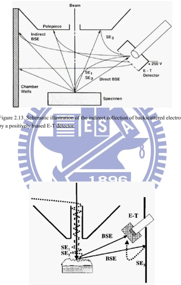
FIGURE 2.13.SCHEMATIC ILLUSTRATION OF THE INDIRECT COLLECTION OF BACKSCATTERED ELECTRONS BY A POSITIVELY BIASED E-T DETECTOR. ... 45
FIGURE 2.14.THROUGH-THE-LENS (TTL) DETECTOR FOR SE USED IN HIGH-PERFORMANCE FIELD
EMISSION SEMS. ... 45
FIGURE 2.15.TYPICAL EXPERIMENTAL SET-UP FOR PL MEASUREMENTS. ... 46
FIGURE 2.16.SCHEMATIC OF THE LUMINESCENCE TRANSITIONS BETWEEN THE CONDUCTION BAND (EC),
VALENCE BAND (EV), EXCITION (EE), DONOR (ED), AND ACCEPTOR (EA) LEVELS IN A LUMINESCENT
MATERIAL. ... 46
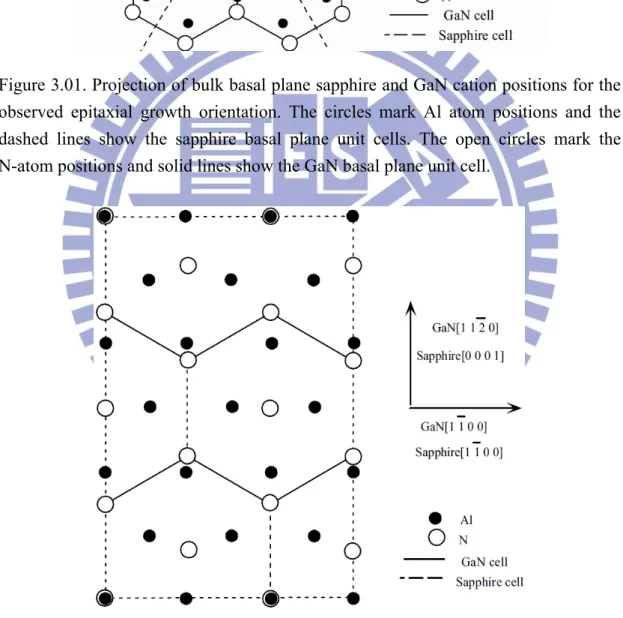
FIGURE 3.01.PROJECTION OF BULK BASAL PLANE SAPPHIRE AND GAN CATION POSITIONS FOR THE OBSERVED EPITAXIAL GROWTH ORIENTATION.THE CIRCLES MARK AL ATOM POSITIONS AND THE DASHED LINES SHOW THE SAPPHIRE BASAL PLANE UNIT CELLS.THE OPEN CIRCLES MARK THE
N-ATOM POSITIONS AND SOLID LINES SHOW THE GAN BASAL PLANE UNIT CELL. ... 59
FIGURE 3.02.PROJECTION OF BULK A-PLANE SAPPHIRE AND BASAL PLANE GAN CATION POSITIONS FOR THE OBSERVED EPITAXIAL GROWTH ORIENTATION.THE SOLID CIRCLES MARK THE AL ATOM POSITIONS AND THE DASHED LINES SHOW THE SAPPHIRE A-PLAN UNIT CELLS.THE OPEN CIRCLES MARK THE N-ATOM POSITIONS AND THE SOLID LINES SHOW THE GAN BASAL PLANE UNIT CELL. ... 59
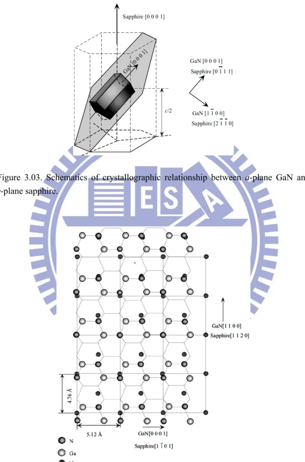
FIGURE 3.03.SCHEMATICS OF CRYSTALLOGRAPHIC RELATIONSHIP BETWEEN A-PLANE GAN AND Γ-PLANE SAPPHIRE. ... 60
FIGURE 3.04.PROJECTION OF BULK Γ-PLANE SAPPHIRE AND A-PLANE GAN ANION AND CATION POSITIONS FOR THE OBSERVED EPITAXIAL GROWTH ORIENTATION. ... 60
FIGURE 3.05.(A)SAPPHIRE Γ-PLANE STACKING SEQUENCE SHOWING O ATOMS IN LARGER CLEAR CIRCLES AND AL ATOMS IN SMALLER, FILLED CIRCLES.(B)THE ATOMIC ARRANGEMENT ON THREE LAYERS
(THE UPPERMOST ONE IS O, IMMEDIATELY BELOW IS AL AND THIRD LAYER DOWN IS ANOTHER O
LAYER) ON THE Γ-PLANE OF SAPPHIRE. ... 61
FIGURE 3.06.DEPICTION OF C-PLANE, A-PLANE, M-PLANE, Γ-PLANE IN GAN. ... 62
FIGURE 3.07.TRENCH-PATTERNED M-PLANE SAPPHIRE SUBSTRATE FOR A-PLANE GAN OVERGROWTH. .. 62
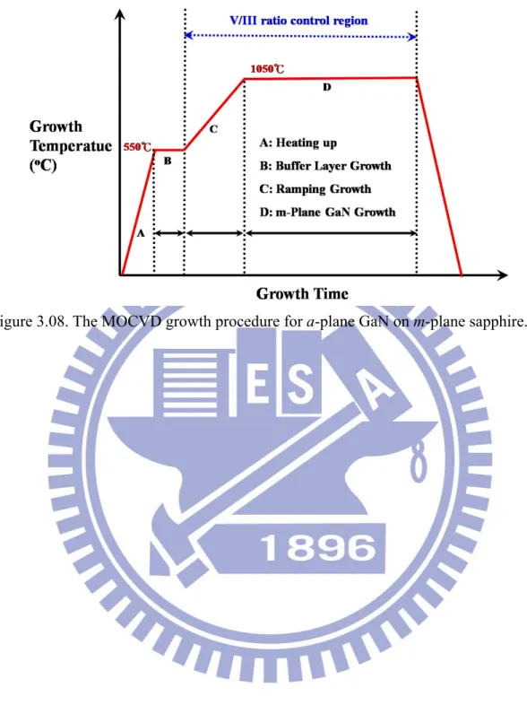
FIGURE 3.08.THE MOCVD GROWTH PROCEDURE FOR A-PLANE GAN ON M-PLANE SAPPHIRE. ... 63
FIGURE 3.09.SCHEMATICS OF TELOG A-PLANE GAN TECHNIQUE. ... 64
FIGURE 3.10.THE MOCVD GROWTH PROCEDURE FOR A-PLANE GAN BY TELOG TECHNIQUE. ... 65
FIGURE 3.11.CONDITIONS OF KOH ETCHING OF TELOG A-PLANE GAN AND INGAN/GANMQWS. ... 65
FIGURE 4.01.XRD Θ-2Θ SPECTRUM OF A-PLANE EPITAXY ON TRENCH-PATTERNED M-PLANE SAPPHIRE. . 72
FIGURE 4.03.THE SEM IMAGES OF A-PLANE GAN GROWN BY MOCVD ON TRENCH-PATTERNED M-PLANE SAPPHIRE UNDER THE V/III RATIO OF 1800. ... 73
FIGURE 4.04.THE SEM IMAGES OF A-PLANE GAN GROWN BY MOCVD ON TRENCH-PATTERNED M-PLANE SAPPHIRE UNDER THE V/III RATIO OF 350. ... 73
FIGURE 4.05.THE SEM IMAGES A-PLANE GAN GROWN BY MOCVD ON TRENCH-PATTERNED M-PLANE SAPPHIRE UNDER THE V/III RATIO OF 9000.THE CORRESPONDING CRYSTAL PLANES AND ORIENTATIONS ARE DEPICTED. ... 74
FIGURE 4.06.THE SEM IMAGES OF A-PLANE GAN GROWN BY MOCVD ON TRENCH-PATTERNED M-PLANE SAPPHIRE UNDER THE V/III RATIO OF 1800.THE CORRESPONDING CRYSTAL PLANES AND ORIENTATIONS ARE DEPICTED. ... 74
FIGURE 4.07.THE SEM IMAGES OF A-PLANE GAN GROWN BY MOCVD ON TRENCH-PATTERNED M-PLANE SAPPHIRE UNDER THE V/III RATIO OF 350.THE CORRESPONDING CRYSTAL PLANES AND ORIENTATIONS ARE DEPICTED. ... 75
FIGURE 4.08.SCHEMATICS OF THE EPITAXIAL MODE OF A-PLANE GAN ON M-PLANE SAPPHIRE UNDER THE V/III RATIO OF 9000 BY MOCVD. ... 75
FIGURE 4.09.SCHEMATICS OF THE EPITAXIAL MODE OF A-PLANE GAN ON M-PLANE SAPPHIRE UNDER THE V/III RATIO OF 1800 BY MOCVD. ... 76
FIGURE 4.10.SCHEMATICS OF THE EPITAXIAL MODE OF A-PLANE GAN ON M-PLANE SAPPHIRE UNDER THE
V/III RATIO OF 350 BY MOCVD. ... 76
FIGURE 4.11.THE SEM IMAGES OF A-PLANE GAN GROWN BY MOCVD ON TRENCH-PATTERNED M-PLANE SAPPHIRE UNDER THE V/III RATIO OF 72. ... 77
FIGURE 4.12.THE SEM IMAGES OF A-PLANE GAN GROWN BY MOCVD ON TRENCH-PATTERNED M-PLANE SAPPHIRE UNDER THE V/III RATIO OF 72.THE CORRESPONDING CRYSTAL PLANES AND
ORIENTATIONS ARE DEPICTED. ... 77
FIGURE 4.13.THE CROSS-SECTIONAL TEM IMAGE OF GAN GROWN BY MOCVD UNDER THE V/III RATIO OF 72 WITH TERRACE/TRENCH WIDTH 2ΜM/4ΜM.THE CORRESPONDING CRYSTAL PLANES AND ORIENTATIONS ARE DEPICTED. ... 78
FIGURE 4.14.THE CROSS-SECTIONAL TEM IMAGE OF GAN GROWN BY MOCVD UNDER THE V/III RATIO OF 72 WITH TERRACE/TRENCH WIDTH 2ΜM/4ΜM.THE CORRESPONDING CRYSTAL PLANES,
ORIENTATIONS AND DEFECTS DISTRIBUTION ARE DEPICTED... 78
FIGURE 4.15.THE CROSS-SECTIONAL TEM IMAGE OF GAN GROWN BY MOCVD UNDER THE V/III RATIO OF 72 WITH TERRACE/TRENCH WIDTH 2ΜM/4ΜM.THE CORRESPONDING G VECTOR IS ALONG [0001] DIRECTION. ... 79
FIGURE 4.16.THE CROSS-SECTIONAL TEM IMAGE OF GAN GROWN BY MOCVD UNDER THE V/III RATIO OF 72 WITH TERRACE/TRENCH WIDTH 2ΜM/4ΜM.THE CORRESPONDING G VECTOR IS ALONG [-2110]
DIRECTION. ... 79
FIGURE 4.17.THE CL IMAGES OF A-PLANE GAN GROWN BY MOCVD ON TRENCH-PATTERNED M-PLANE SAPPHIRE UNDER THE V/III RATIO OF 1800. ... 80
FIGURE 5.01.THE SEM IMAGES OF A-PLANE GAN GROWN BY MOCVD USING TELOG TECHNIQUE UNDER THE V/III RATIO OF 500 AND 980°C.THE CORRESPONDING CRYSTAL PLANES AND
ORIENTATIONS ARE DEPICTED.GROWTH TIME IS 30 MIN. ... 91
FIGURE 5.02.THE SEM IMAGES OF A-PLANE GAN GROWN BY MOCVD USING TELOG TECHNIQUE UNDER THE V/III RATIO OF 500 AND 980°C.THE CORRESPONDING CRYSTAL PLANES AND
ORIENTATIONS ARE DEPICTED.GROWTH TIME IS 120 MIN. ... 91
FIGURE 5.03.THE SEM IMAGES OF A-PLANE GAN GROWN BY MOCVD USING TELOG TECHNIQUE UNDER THE V/III RATIO OF 72 AND 980°C.THE CORRESPONDING CRYSTAL PLANES AND
ORIENTATIONS ARE DEPICTED.GROWTH TIME IS 120 MIN. ... 92
FIGURE 5.04.THE SEM IMAGES OF PLANAR A-PLANE GAN GROWN BY MOCVD USING TELOG
TECHNIQUE UNDER THE V/III RATIO OF 72 AND 980°C.THE CORRESPONDING SEED REGION AND THE
LATERAL WING REGION ARE DEPICTED. ... 92
FIGURE 5.05.THE TEM IMAGES OF A-PLANE GAN GROWN BY MOCVD USING TELOG TECHNIQUE UNDER THE V/III RATIO OF 72 AND 980°C.THE CORRESPONDING SEED REGION, LATERAL WING REGION AND THE DISTRIBUTION OF DISLOCATIONS ARE DEPICTED. ... 93
FIGURE 5.06.THE TEM IMAGES OF A-PLANE GAN GROWN BY MOCVD USING TELOG TECHNIQUE UNDER THE V/III RATIO OF 72 AND 980°C.THE CORRESPONDING COALESCENCE BOUNDARY
BETWEEN +C-PLANE AND –C-PLANE IS DEPICTED. ... 93
FIGURE 5.07.XRD Ω-2Θ SPECTRUM ALONG [0001] DIRECTION OF A-PLANE GAN TEMPLATE AND TELOG A-PLANE GAN ON Γ-PLANE SAPPHIRE. ... 94
FIGURE 5.08.XRD Ω-2Θ SPECTRUM ALONG [1-100] DIRECTION OF A-PLANE GAN TEMPLATE AND TELOG A-PLANE GAN ON Γ-PLANE SAPPHIRE. ... 94
FIGURE 5.09.XRD Ω-2Θ SPECTRUM ALONG [0001] DIRECTION OF TELOG A-PLANE INGAN/GANMQWS ON Γ-PLANE SAPPHIRE. ... 95
FIGURE 5.10.XRD Ω-2Θ SPECTRUM ALONG [1-100] DIRECTION OF TELOG A-PLANE INGAN/GAN MQWS ON Γ-PLANE SAPPHIRE. ... 95
FIGURE 5.11.THE CL MAPPING IMAGE AT EMISSION ENERGY OF GAN OF THE TELOG A-PLANE GAN AND THE CORRESPONDING SEM IMAGE.THE CORRESPONDING SEED AND WING REGIONS ARE DEPICTED.
... 96
FIGURE 5.12.THE CL MAPPING IMAGE AT EMISSION ENERGY OF INGAN/GANMQWS OF THE TELOG
REGIONS ARE DEPICTED. ... 97
FIGURE 5.13.THE TEM IMAGES OF INGAN/GANMQWS GROWN BY MOCVD USING TELOG
TECHNIQUE UNDER THE V/III RATIO OF 72 AND 980°C.THE CORRESPONDING SEED REGION,
LATERAL WING REGION AND THE DISTRIBUTION OF DISLOCATIONS ARE DEPICTED. ... 98
FIGURE 5.14.THE TEM IMAGES OF INGAN/GANMQWS GROWN BY MOCVD USING TELOG
TECHNIQUE UNDER THE V/III RATIO OF 72 AND 980°C ON THE SEED REGION. ... 98
FIGURE 5.15.THE TEM IMAGES OF INGAN/GANMQWS GROWN BY MOCVD USING TELOG
TECHNIQUE UNDER THE V/III RATIO OF 72 AND 980°C ON THE WING REGION. ... 99
FIGURE 5.16.THE CL MAPPING IMAGE AT EMISSION ENERGY OF BOTH INGAN/GANMQWS AND GAN OF THE TELOG A-PLANE GAN.THE PEAK POSITION WHICH CORRESPONDS TO SEED AND WING
REGIONS ARE DEPICTED. ... 99
FIGURE 6.01.SCHEMATIC DIAGRAMS OF THE GAN VIEWED ALONG THE [-1-120] FOR N-POLAR GAN TO EXPLAIN THE MECHANISM OF THE POLARITY-SELECTIVE CHEMICAL ETCHING. ... 118
FIGURE 6.02.SCHEME OF ETCHING MECHANISM OF GAN(1-100) M-PLANE IN TOP AND SIDE VIEWS. .... 119
FIGURE 6.03.SCHEME OF ETCHING MECHANISM OF GAN(11-20) A-PLANE IN TOP AND SIDE VIEWS. ... 120
FIGURE 6.04.SEM IMAGES OF THE AIR-VOIDS IN TELOG A-PLANE GAN UNDER DIFFERENT ETCHING CONDITIONS AT ETCHING TIME 10 MIN. ... 121
FIGURE 6.05.SEM IMAGES OF THE AIR-VOIDS IN TELOG A-PLANE GAN UNDER DIFFERENT ETCHING CONDITIONS AT ETCHING TIME 20 MIN. ... 121
FIGURE 6.06.SEM IMAGES OF THE AIR-VOIDS IN TELOG A-PLANE GAN UNDER DIFFERENT ETCHING CONDITIONS AT ETCHING TIME 40 MIN. ... 122
FIGURE 6.07.SEM IMAGES OF THE AIR-VOIDS IN TELOG A-PLANE GAN UNDER DIFFERENT ETCHING CONDITIONS AT ETCHING TIME 80 MIN. ... 122
FIGURE 6.08.THE SUMMARY OF THE ETCHING RESULTS UNDER DIFFERENT ETCHING CONDITIONS.THE THRESHOLD-TIMES NEEDED TO GET THE ISOSCELES TRIANGLE ARE SHOWN. ... 123
5 WT.% AND 100°C. ... 123
FIGURE 6.10.TIME-DEPENDENT SEM IMAGES OF THE AIR-VOIDS IN TELOG A-PLANE GAN UNDER KOH 5 WT.% AND 120°C. ... 123
FIGURE 6.11.TIME-DEPENDENT SEM IMAGES OF THE AIR-VOIDS IN TELOG A-PLANE GAN UNDER KOH 10 WT.% AND 120°C. ... 124
FIGURE 6.12.TIME-DEPENDENT SEM IMAGES OF THE AIR-VOIDS IN TELOG A-PLANE GAN UNDER KOH 20 WT.% AND 120°C. ... 124
FIGURE 6.13.TIME-DEPENDENT SEM IMAGES OF THE AIR-VOIDS IN TELOG A-PLANE GAN UNDER KOH 5 WT.% AND 140°C. ... 124
FIGURE 6.14.TIME-DEPENDENT SEM IMAGES OF THE AIR-VOIDS IN TELOG A-PLANE GAN UNDER KOH 10 WT.% AND 140°C. ... 124
FIGURE 6.15.TIME-DEPENDENT SEM IMAGES OF THE AIR-VOIDS IN TELOG A-PLANE GAN UNDER KOH 20 WT.% AND 140°C. ... 125
FIGURE 6.16.TIME-DEPENDENT SEM IMAGES OF THE AIR-VOIDS IN TELOG A-PLANE GAN UNDER KOH 10 WT.% AND 120°C.THE CORRESPONDING ETCHING GEOMETRIES AND THE RELATED CRYSTALLINE DIRECTIONS ARE DEPICTED. ... 125
FIGURE 6.17.SCHEMATIC IMAGES OF THE AIR-VOIDS IN TELOG A-PLANE GAN UNDER KOH SOLUTIONS.
THE CORRESPONDING ETCHING GEOMETRIES AND THE RELATED TIME ARE DEPICTED. ... 126
FIGURE 6.18.SEM IMAGES OF THE AIR-VOIDS IN TELOG A-PLANE GAN UNDER KOH20 WT.% AND
120°C.THE ETCHING TIME IS 160 MIN. ... 126
FIGURE 6.19.SEM IMAGES OF THE AIR-VOIDS IN TELOG A-PLANE GAN UNDER KOH5 WT.% AND 140°C.
THE ETCHING TIME IS 40 MIN. ... 127
FIGURE 6.20.SEM IMAGES OF THE ORIGINAL AIR-VOIDS IN TELOG A-PLANE GAN. ... 127
FIGURE 6.21.THE METHODS OF DETERMINING THE ETCHING RATE OF THE AIR-VOIDS IN TELOG A-PLANE
GAN UNDER KOH ETCHING. ... 128
ETCHING CONDITIONS. ... 128
FIGURE 6.23.PL SPECTRUM OF THE TELOG A-PLANE 440NM INGAN/GANMQWS AFTER DIFFERENT
KOH ETCHING TIME.THE DETECTOR WAS LOCATED NORMAL TO THE TELOG A-PLANE SAMPLE. 129
FIGURE 6.24.THE TRACEPRO MODEL TO SIMULATE THE EFFECTS OF THE AIR-VOIDS ON THE LIGHT TRAJECTORIES. ... 129
FIGURE 6.25.THE TRACEPRO SIMULATION RESULT OF THE EFFECTS OF THE AIR-VOIDS ON THE LIGHT TRAJECTORIES. ... 130
FIGURE 6.26.ROOM TEMPERATURE PL INTENSITY AT VARIED ANGLE.THE ANGLE VARIATION WAS
Chapter 1
Introduction
1.1 Perspectives of Group-III Nitrides and Light-Emitting
Diodes (LED)
Starting with the pioneering work of Maruska et al. on GaN in the late 1960s and early 1970s with hydride vapor-phase epitaxial growth [1.01, 1.02] and continuing with the subsequent major breakthrough by Amano et al. in the 1980s on two-step growth and p-type GaN activation [1.03, 1.04], and then by Nakamura et al. in the early to mid 1990s [1.05~1.09], nearly all work on GaN-based materials and devices has been on c-plane (0001)-oriented layers. Due to the inability to fabricate bulk GaN crystal at the time of early GaN pioneering work, an area that still remains a major challenge for nitride research, GaN-based technology, has been developed on foreign substrates. The highest quality GaN has been grown in the (0001) orientation on either (0001)-oriented sapphire or (0001)-oriented 4H-SiC or 6H-SiC.
At the mid-to-late 1990s, Nakamura was making major breakthrough in the GaN-based materials and devices. At the same time, Resta [1.10] and Vanderbilt and Kingsmith [1.11, 1.12] were developing the quantum theory of polarization. In their landmark Vanderbilt and Kingsmith showed that polarization in a sokid is a bulk property and can be determined quantum mechanically with knowledge of the phase of the valence electron wave function. Subsequently, Bernardini et al. [1.13] calculated the spontaneous polarization and piezoelectric constants of GaN, AlN, and InN; this
work is the standard used currently for these important physical properties in Group-III nitrides.
In 2000, Waltereit et al. in Kaus Ploog’s group at the Paul Drude Institute in Berlin reported on the first planar nonpolar (10-10) m-plane film on (100)-oriented γ-LiAlO2 substrate [1.14]. In their breakthrough article Waltereit et al. demonstrated the
absence of internal electric field in m-plane GaN quantum wells with AlGaN barriers. This work motivated a worldwide research effort in nonpolar and semipolar nitrides.
In 2001~2002, researchers at the UCSB and elsewhere learned that Group-III nitrides growth on γ-plane (10-12) sapphire yields a-plane {11-20} film with only film orientation; however, previous growth efforts always yielded rough films with faceted three-dimensional morphologies [1.15, 1.16]. Craven et al. [1.15] discovered by MOCVD growth and Ng [1.16] realized by molecular beam epitaxy planar a-plane films on γ-plane (10-12) sapphire. Until recently, the γ-plane was the most common orientation for sapphire substrate, and thus Craven’s and Ng’s results provided a pathway to large-area low-cost nonpolar films.
In 2005, using defective m-plane GaN-based LEDs grown on m-plane SiC, Gardner et al. demonstrated another interesting feature of nonpolar structure i.e. polarized light emission [1.17]. The potential for engineering In1-xGaxN quantum wells
in nonpolar orientations for polarized light emission and detection has been an active area of research.
During 2005~2006, there was a transformation in nonpolar and semipolar GaN research. Researcher at Furukawa Company and at Mitsubishi Chemical Corporation developed several millimeters thick c-plane GaN boules by HVPE [1.18]. Subsequently,
low defect density nonpolar and semipolar GaN substrate can be prepared by wafering these boules in a suitable orientation. The group at Rohm and at UCSB has produced nonpolar and semipolar LEDs that rival the performance of state-of-art c-plane devices. The Rohm and UCSB groups demonstrated the first nonpolar laser diodes and the first AlGaN clad-free laser diodes [1.19].
The promise of nonpolar light emitters has now been realized. In the coming year, we will learn whether nonpolar structures will be the ultimate solution for realizing nitride emitters at many different wavelengths and for a variety of electron devices.
1.2 Specific Properties of Group-III Nitride (GaN) and LED
Application
The Group-III nitrides are a remarkable materials system. With direct bandgap from 0.7 eV (InN) through 3.4 eV (GaN) to 6.0 eV (AlN), this materials system has enable deep ultraviolet (λ < 300nm or photon energy > 4.1 eV based on high Al content AlxGa1-xN quantum wells), ultraviolet (λ < 400nm or photon energy > 3.1 eV),
blue (λ = 455nm or photon energy = 2.7 eV based on InxGa1-xN quantum wells), green
(λ = 525nm or photon energy = 2.4eV) emitters based on InxGa1-xN quantum wells,
and longer wavelength light-emitting diodes. No other materials system offers the range of direct bandgap.
Prior to the development of the nitrides as optoelectronic materials, there were no efficient ultraviolet and blue LEDs. Devices based on Group-III nitrides perform well
despite the threading dislocation densities typically in excess of 108 cm-2 in comparison to conventional III-V materials such as GaAs, where the dislocation densities are typically 104 cm-2 or less. However, when the nitrides are remarkably robust against oxidation, they are mechanically hard and show no evidence for extended defect motion at standard operation temperatures. GaN-based LEDs feature prominently in colored lighting application, such as green traffic light. When blue LEDs are combined with a yellow-emitting phosphor, white light is produced; thus GaN has become the material that enabled the field of solid-state lighting. Violet GaN-based laser diodes operating at a wavelength of 405nm are already in broad use in high definition optical data storage.
Through the mid-to-late 1990s, there was a broadening realization of the importance of piezoelectricity and polarization in Group-III nitrides [1.20~1.23]. Since the wurtzite structure (hexagonal, space group P63mc, point group 6mm) is
noncentrosymmetric i.e. absence of inversion symmetry, it is polar, with spontaneous polarization occurring parallel to the –c-axis. Polarization-related effects are a dominant feature in common c-axis GaN-based heterostructures and a major differentiating feature of the wurtzite Group-III nitrides from other well-developed semiconductors, such as silicon or gallium arsenide.
For light emitting diodes based on GaN barriers and InxGa1-xN quantum wells,
the fixed charge at the heterostructure cause large electric field normal to the quantum well plane that are in the opposite sense to the polarization-related electric fields in Al1-xGaxN/GaN system. The difference in spontaneous polarization between
InxGa1-xN and GaN is small, but the InxGa1-xN layer are coherently strained and large
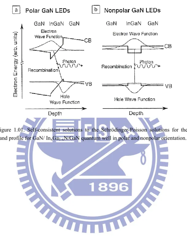
1.01, which were produced by self-consistent solutions to the Schrödinger and Poisson equations. In optoelectronic devices such as LEDs, the InxGa1-xN quantum
wells are placed in the depletion region of a p-n diode such that injected electrons and holes are captured by the quantum well without recombination in the surrounding materials. These internal polarization-related electric field causes spatial separation of electron and hole wave functions. When the electron and hole wave functions are spatially separated due to the internal polarization-related electric field in the quantum well (quantum-confined Stark effect [QCSE]), the likelihood of a radiative recombination event, which yields the desired photon, is reduced, and thus there is increased likelihood of the injected electrons or holes to nonradiatively recombine and the energy is squandered as heat. Thus, the polarization-related electric fields are seen to reduce efficiency in nitride LEDs and laser diodes.
The challenges associated with polar heterostructure in the nitrides could be avoided entirely by growth in nonpolar orientation (i.e. with the c-axis of wurtzite structure parallel to any heterojunction). Due to the crystal symmetry, there would be no polarization discontinuity to at the heterointerface. The low index a-plane {11-20} and m-plane {10-10} are candidate orientations for fabricating nonpolar heterostructures.
The absence of the polarization field effect in nonpolar quantum wells was confirmed by the distinctly short rediative lifetime of m-plane AlGaN/GaN quantum wells compared with the c-plane radiative lifetime because in the nonpolar quantum wells, the electron an hole wave function have strong overlap, whereas in the c-plane quantum wells, the wave functions are spatially separated [1.14]. At the same time, the cathodoluminescence peak energy of m-plane quantum well was higher than that of
c-plane quantum well, which was explained purely by the quantum size effect. After the finding, a similar absence of the QCSE has been reported for a-plane AlGaN/GaN quantum wells in a-plane GaN [1.16, 1.24].
1.3 Motivation and Organization of the Thesis
Light emitting diodes (LEDs), in particular the Group-III nitride LEDs, have advanced from being low-power indicators to high-power, high-brightness lighting sources. To harness the full potential of it for next-generation solid-state lighting, further increasing in the quantum efficiency is required.
The lighting efficiency of LEDs is determined by mainly two most important factors: the internal quantum efficiency and the light extraction efficiency. The internal quantum efficiency is defined as the ratio of the number of injected electron-hole pairs to that of generated electrons. The light extraction efficiency is defined as the ratio of the number of generated photons to the number extracted from the devices.
As the aforementioned, quantum-confined Stark effect (QCSE) plays an important role in the realm of the Group-III nitride LEDs, especially the InGaN/GaN based LEDs. The nonpolar Group-III nitride materials have approved to overcome the effects of internal electric fields which are caused by the asymmetry of the Group-III nitride crystalline structure. In this thesis, the first part of the research is focusing on the MOCVD growth techniques and the substrate engineering to try to realize a
nonpolar, high quality nonpolar a-plane GaN on the patterned m-plane sapphire. The results are available in chapter 4. Properties including the substrate engineering method, MOCVD growth modes, and crystalline quality inspection of a-plane GaN, the defects distribution and optical properties of the a-plane GaN epitaxy are investigated in detail. The experiments in this chapter give great learning of the senses and are a critical guidance to the further experiments.
Still we pay attention to the nonpolar a-plane GaN. In chapter 5, a complete planar a-plane GaN on patterned a-plane GaN tamplates on γ-plane sapphire by techniques of trenched epitaxial lateral overgrowth (TELOG) is achieved. And at the same time InGaN/GaN multiple quantum wells (MQWs) are grown on it. As the same in chapter4, the substrate engineering methods, the MOCVD growth modes, the inspections of crystalline qualities including SEM, XRD and TEM images are available. Meanwhile, optical properties including PL and CL of the a-plane GaN and the InGaN/GaN MQWs are measured.
So far, by the experiments and results in chapter 4 and 5, the polarity issues of Group-III nitride materials have been overcome. However, the light extraction efficiency is still a problem. Most of the generated photons remain in the LED owing to total internal reflection at its surface, arising because of the large refractive index difference between the semiconductor and air. This causes the ultra-low light extraction efficiency and leads to a low external quantum efficiency.
The fact strongly indicates that some air-voids in the Group-III nitride materials especially the interfaces of different materials would make improvements to the light extraction efficiency at a certain level. Thus we introduce some air-voids into the TELOG a-plane GaN and expecte it would help in modifying the light-propagation
direction and helps more photons to leave the devices and thus increasing the light-extraction efficiency.
Although there are various competitive methods for improving light extraction efficiency in LEDs, including the introduction of surface roughness, the use of a patterned substrate and chip shaping, here in chapter 6 of the thesis we use KOH-ethylene glycol solution to enlarge the initial voids in the a-plane GaN which was formed during the MOCVD growth periods by TELOG techniques. The etching mechanisms under different etching condition are clarified and the etching rates have been determined. What’s more, the effect of these etched air-voids on the enhancement of light extraction efficiency is measured. We successfully achieve the redistribution of the light emission and gain a significant increase in the emission intensity at certain ranges of angle.
Brief conclusions and future works are available in chapter 7, which will fulfill the related experiments and give a further potential application of the results in this thesis.
1.4 References
[1.01]H. P. Maruska, J. J. Tietjen, Appl. Phys. Lett. 15, 327 (1969)
[1.02]H. P. Maruska, D. A. Stevenson, J. I. Pankov, Phys. Lett. 22, 303 (1973) [1.03]H. Amano, N. Sawaki, I. Akasaki, Y. Toyoda, Phys. Lett. 48, 333 (1986) [1.04]H. Amano, M. Kito, K.I. Hiramatsu, I. Akasaki, Jpn. J. Phys. Lett. 28,
L2112 (1989)
[1.06]S. Nakamura, T. Mukai, M. Senoh, Jpn. J. Phys. Lett. 30, L1998 (1991) [1.07]S. Nakamura, N.Iwasa, T. Mukai, M. Senoh, Jpn. J. Phys. Lett. 31, L1258
(1992)
[1.08]S. Nakamura, T. Mukai, M. Senoh, Appl. Phys. Lett. 64, 1687 (1994) [1.09]S. Nakamura, M. Senoh, S. Nagahama, N.Iwasa, T. Yamada, T. Matsushita,
H. KIyoku, Y.Sugimoto, Jpn. J. Phys. Lett. 35, L74 (1996) [1.10]R. Resta, Ferroelectrics 136, 51 (1992)
[1.11]R. D. Kingsmith, D. Vanderbilt, Phys. Rev. B 47, 1651 (1993) [1.12]D. Vanderbilt, R. D. Kingsmith, Phys. Rev. B 48, 4442 (1993)
[1.13]F. Bernardini, F. Fiorentini, D. Vanderbilt, Phys. Rev. B 56, 10024 (1997) [1.14]P. Waltereit, O. Brandt, A. Trampert, H. T. Grahn, J. Meeiger, M.
Ramsteiner, M. Reiche, K. H. Ploog, Nature 406, 865 (2000)
[1.15]M. D. Craven, S. H. Lim, F. Wu, J. S. Speck, S. P. DemBaars, Appl. Phys. Lett. 81, 469 (2002)
[1.16]H. M. Ng, Appl. Phys. Lett. 80, 4369 (2002)
[1.17]N. F. Gardner, J. C. Kim, J. J. Wierer, Y. C. Shen, M. R. Krames, Appl. Phys. Lett. 86, 111101 (2002)
[1.18]M. Funato, M. Ueda, Y. Kawakami, Y. Narukawa, T. Kosugi, M. Takahashi, T. Mukai, Jpn. J. Phys. Lett. 45, L659 (2006)
[1.19]D. F. Feezell, M. C. Schmidt, R. M. Farrell, K. C. Kim, M. Saito, K. Fujito, D. A. Cohen, J. S. Speck, S. P. DemBaars, S. Nakamura, Jpn. J. Phys. Lett.
46, L284 (2007)
[1.20]A. Byhovski, B. Gelmont, M. Shur, J. Appl. Phys. 74, 6734 (1993)
[1.21]S. Chichibu, T. Azuhata, T. Sato, S. Nakamura, Appl. Phys. Lett. 69, 4188 (1996)
I. Akasaki, Jpn. J. Phys. Lett. 36, L382 (1997)
[1.23]J. S. Im, H. Kollmer, J. Off, A. Sohmer, F. Scholz, A. Hangleiter, Phys. Rev. B 57, R9435 (1998)
[1.24]T. Koida, S.F. Chichibu, T. Sato, M. D. Craven, B. A. Haskell, J. S. Speck, S. P. DemBaars, S. Nakamura, Appl. Phys. Lett. 84, 3768 (2004)
Figure 1.01. Self-consistent solutions to the Schrödinger-Poisson solutions for the band profile for GaN/ InxGa1-xN/GaN quantum well in polar and nonpolar orientation.
Chapter 2
Experimental Apparatus
2.1 Sapphire Substrate
The crystal lattice of crystalline sapphire is formed by Al3+ and O2− ions. If the O2− anions are depicted as balls, the crystal lattice takes the form of their closest hexagonal packing in figure 2.01. The Al3+ cations are located in a crystalline field that has no symmetry center (due to crystal lattice distortions). These cations lie in the octahedral hollows between the closely packed O2− ions, filling two thirds of these hollows. The octahedron hollow is surrounded by six balls. If the radius of each is taken as a unit, then the hollow contains a ball with a relative radius of 0.41. Due to the ratio of the ionic radii of O2− and Al3+ (equal to 1.40 and 0.57 Å, respectively), the cations are located within the hollows of the anion packing. They slightly distort the lattice, but do not fall outside the stability limits of the octahedron position.
Lattice parameters, or hexagonal lattice constants of crystalline sapphire are a = b and c, and the interplanar distances are given by the equation 2.01
dhkl =1 / [(4/3α2)(h2+k2+hk) + (1+1/c2)l2]1/2 (2.01)
The values of the interplanar distances are presented in Table 2.01. The lattice parameters increase with increasing temperature. At 295.65K a=4.759213Å, c=12.991586 Å [2.01], and the ratio c/a=2.729776 far exceeds that of a crystal with ideal hexagonal packing (8/3)0.5=1.633. Precise measurements of the temperature
dependence of the lattice parameters within 4.5~374K temperature range in figure 2.02 were carried out using 57Fe Mössbauer radiation [2.02].
Cleavage in sapphire arises at the intersections of a pair of parallel nets formed by anions. Nets with like charges reduce attractive forces. The larger the distance between the nets, the more vividly the cleavage manifests itself. In a perfect crystal the plane of chipping must pass between these nets. In the basal plane with interchanging O–Al–Al–O–Al–O layers there are no conditions for cleavage, whereas in the plane (10-11) with interchanging O–O–Al–O–Al–O–O—O–Al–O–Al–O layers the bonds between the layers O–O located at a distance of 1.06 Å are weakened.
Sapphire does not have such a vivid cleavage as diamond and other crystals. For a long period of time, sapphire was considered to exhibit no cleavage at all. Theoretically, it has nine cleavage planes. Six planes are parallel to the facets {11-20}and {10-11}, and to the c-axis; three planes are parallel to the facets {10-11} and inclined to the c-axis at an angle of 33°, the normal vectors to them make an angle of 57° with the C-axis. Crystals with a small quantity of dislocations and which do not contain blocks may have perfect cleavage in the plane of the morphological rhombohedron {10-11}. However, when block-containing and stressed crystals grown by the Verneuil method are chipped along the prismatic planes, mirror chips with steps of several atomic parameters are often observed as in figure 2.03. To achieve more desirable chipping of these crystals, the direction of the c-axis is set at an angle 57° to the crystal growth axis at the location of the prism and rhombohedron planes, as shown in figure 2.03 [2.03].
The energy required for destruction along the plane {10-11} is 6 J/m2, whereas for the basal plane the corresponding value is more than 40 J/m2 [2.04]. Shown by the
estimation of the surface energy of the planes, considered to be defined by the quantity of free bonds per unit of surface, the minimum quantity of such bonds corresponds to the plane (10-11) [2.05].
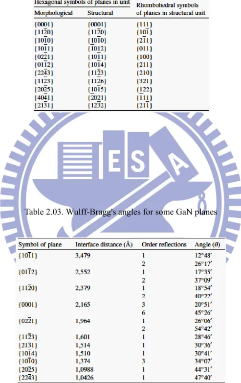
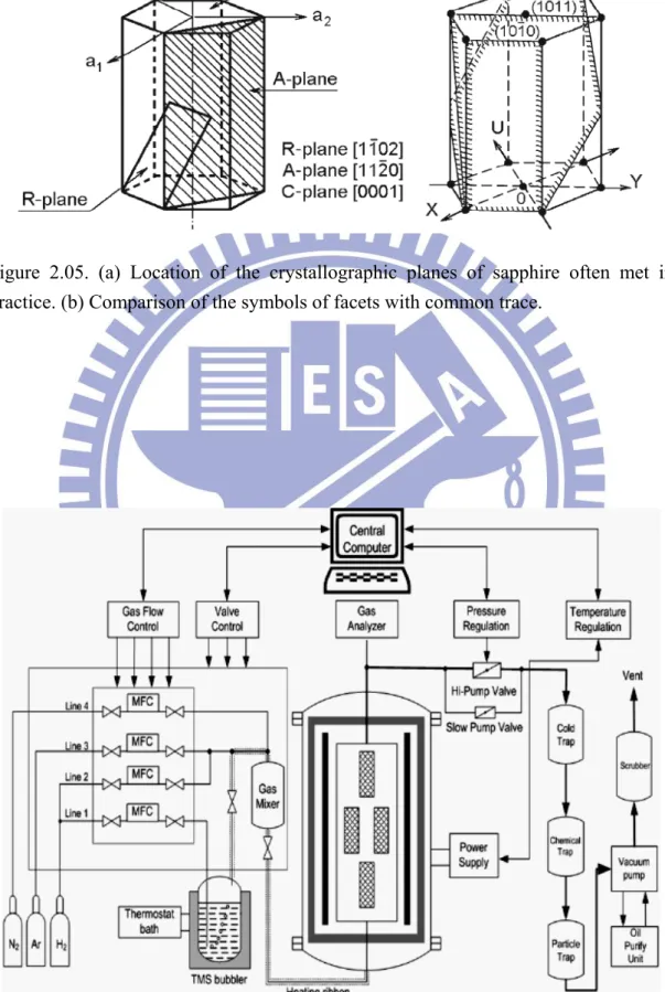
The shape of natural crystals usually has the following facets (denoted by the most often used literal symbols): c(0001), a{11-20}, γ{10-11}, n{22-43}, m{10-10}, s{02-21}, s{22-43}, R{01-12}, p{11-23}(figure 2.04) and others. The symbols of crystallographic planes in the morphological and the structural classification systems, the stereographic projections of sapphire for some planes are given in Tables 2.02 and 2.03. Besides the main crystallographic planes, tens of others exist which have their own symbols. The main forms with their spherical coordinates are presented in Table 2.04. The planes that are most often encountered in the practice of sapphire usage are shown in Fig. 2.05. The plane (1012) is inclined to (0001) plane at an angle of 57°36’, while with the plane (1120) it makes an angle of 32°24’. The angles between the normals to the facets of sapphire are given in Table 2.05.
2.2 Metalorganic Chemical Vapor Deposition (MOCVD)
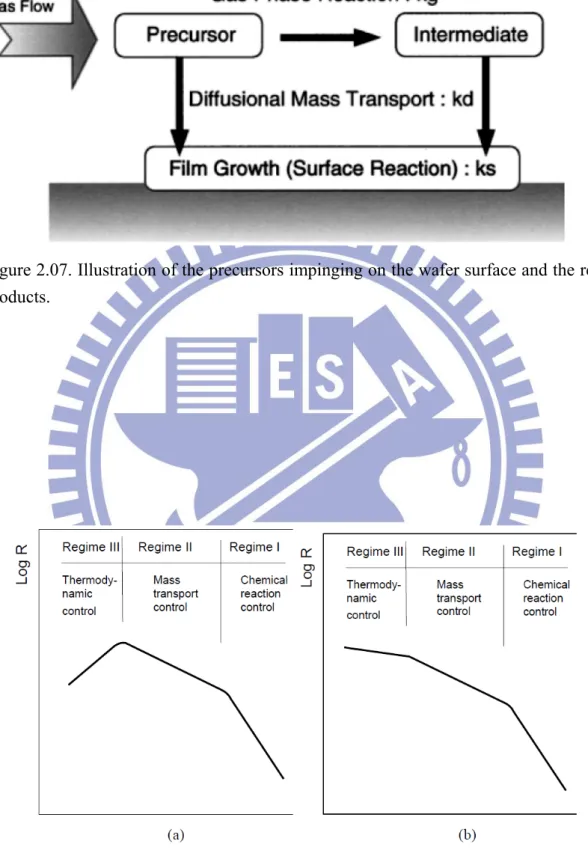
Metalorganic Chemical Vapor Deposition (MOCVD) is the most common epitaxial technique used in both industry and research. It has the benefit of high growth rate on large area wafers. One problem with MOCVD is that it requires complicated and sometimes vary hazardous gases in order to produce the epitaxial layer. Compound semiconductors are grown from the surface reaction of organic compounds or metalorganics and hydrides containing the required species. In growing
GaN hydride mixture containing ammonia and trimethyl-gallium (TMGa), highly diluted by hydrogen or nitrogen, is led into the reactor separately. Figure 2.06 shows a schematic drawing of the MOCVD subsystem. The vapor pressure of the MO source is a function of temperature. By placing the MO bottle in a bath containing a mixture of water and glycol, the vapor pressure can be controlled over a wide range of temperature. The carrier gas is “bubbled” through the MO liquid and transport into the line. The amount of vapor transported into the line depends on the flow rate of the carrier gas (Φc), the pressure in the bottle (Pb) and the vapor pressure Pvap of the MO
(ΦMO). When growing epitaxial films in the reactor, it is of great importance to know
how much source material is introduced. Since the volume and the temperature of the source bottle is constant, the perfect gas law can be used to determine the flow rate of MO (ΦMO). During a time interval Δt, ΦMO.Δt α n moles of source material is defined
from the bottle. According to the perfect gas law
(2.02) where Pc is the partial pressure of the carrier gas in the bottle. In the gas panel
configuration shown in figure 2.06, the pressure in the bottle is controlled from the following line. The partial pressure of the source gas can be expressed as Pc= Pb-
Pvap. Inserting into equation 2.02 the flow rate of the MO (in cm3/min) can be
evaluated.
The precursor molecules NH3 and TMGa are fed in separately into the reactor chamber. In the reactor reactions take place both on the wafer and before the molecules reach the wafer. Formation of the epitaxial layer occurs by the reaction
Figure 2.07 illustrate the growth process with impinging precursors and rest products. Due to the low cracking efficiency of ammonia and adatom mobility the growth of GaN is carried out at very high temperature around 1000°C ~1100°C to high crystalline quality. Many of the difficulties involving the growth of GaN are due to the high volatility of nitrogen. The pressure of nitrogen in the vapor must not be below a certain value to produce the solid without other phases. If the pressure is too low, a Ga liquid phase is formed resulting in droplet formation on the surface of crystal (GaN + 3/2H2 → Ga + NH3). An alternative precursor to NH3 for atomic nitrogen is
dimethyl-hydrazine [2.06]. It has successively been used for growth of GaN [2.07]. Dimethyl-hydrazine has a relatively low decomposition temperature compared to NH3. At 420°C it decompose up to 50% [2.08], while NH3 only 15% at 950°C [2.09].
One thing to be mentioned is that MOCVD is a diffusion controlled process, as the region II in figure 2.08. This regime appears at moderate temperatures. Compared with the chemical reaction regime the mass transport rate of the reactant gaseous species is much lower than that of the chemical reaction, i.e. hG << kS. The coating
growth is limited by the mass transport from the bulk gas to the substrate surface. In this case a steep concentration gradient within the boundary layer is generated and the reactant gaseous species are nearly consumed on the substrate surface.
In this regime, the temperature dependence of the growth rate becomes mild, which is attributed to the gaseous species diffusivity. The growth rate of the coating increases linearly with the partial pressure increasing of the reactant gaseous species (preact), which is confirmed through experimental work as shown in figure 2.08. The
growth rate is inversely proportional to the total pressure in the system. The mass transport rate can be considerably enhanced through a decrease in the total pressure.
This is the main reason that most CVD processes are operated at reduced pressures. An increase in the gas velocity in the bulk is useful to reduce the thickness of the boundary layer and, hence, results in a more rapid growth rate of coatings.
For the growth of monolithic materials the high growth rate is much more important than the thickness uniformity from an economical view. The MOCVD processes are often performed in the mass transport regime. The higher processing temperatures are used for thermal gradient CVI and forced CVI processes in which fast growth rates are needed to ensure the rapid densification of the composites.
2.3 Inductively Coupled Plasma Reactive Ion Etching
(ICP-RIE)
It has been demonstrated that conventional RIE is perfectly capable of etching sub-100 nm structures. The only limitation is its relatively low etch rate, which is normally less than 200 nm min–1 for Si. The etching rate in RIE directly depends on plasma density. For the conventional RIE system as shown in Figure 2.09, plasma density increases with increase of RF power. However, increasing RF power will also increase the self-biasing voltage on the cathode where the etching sample is situated. The consequence is the increase of ion bombardment energy, hence deterioration of etching selectivity. This becomes a particularly serious problem in sub-100 nm RIE, because the masking layer is always thin to enable photon or e-beam patterning of polymer resist at sub-100 nm feature dimension.
Inductively coupled plasma (ICP) system has cleverly solved the problem. In an ICP source, the plasma generation is separated from etching chamber, as shown in Figure 2.10. Radio frequency power is coupled into plasma chamber by an induction coil from outside. The sample stage is connected to a second RF power source as an auxiliary RF source to enhance the production of plasma. Electromagnetic field generated by inductive coupling coil can sustain electron cycling movement in plasma for a long period, which has greatly increased ionization probability while keeping the pressure low in the etching chamber. As the sample stage has an independent input of RF power, the self-biasing voltage can be independently controlled. Therefore, an ICP system can produce very high plasma density (>5×1011 cm–3) compared to conventional RIE (108~1010 cm–3), as well as maintain low ion bombardment energy. The conflict between high plasma density and high etch selectivity encountered in conventional RIE systems has been resolved. With such high plasma density and high etching selectivity, high etching rate and deep RIE (DRIE) become possible.
ICP-RIE has been widely used for etching other materials, especially the III-nitride semiconductors. The ICP with high plasma density offers much higher etch rate and selectivity than it is possible by conventional RIE. For example, GaN or sapphire is known to be difficult to etch. With a conventional RIE, the etch rate is less than 5nm min–1. Using an ICP-RIE the etch rate is nearly 10 times enhanced. Inductively coupled plasma systems are widely used to etch III–V semiconductor materials which are of great importance in high frequency and optoelectronic applications currently.
2.4 Potassium Hydroxide (KOH)-Ethylene Glycol Solution
Potassium hydroxide is an inorganic compound with the formula KOH. Along with sodium hydroxide (NaOH), this colorless solid is a prototypical "strong base". It has many industrial and niche applications. Most applications exploit its reactivity toward acids and its corrosive and etching nature to many materials including the GaN semiconductors. Potassium hydroxide can be found in pure form by reacting sodium hydroxide with impure potassium. Potassium hydroxide is usually sold as translucent pellets, which will become tacky in air because KOH is hygroscopic. Consequently, KOH typically contains varying amounts of water (as well as carbonates). Its dissolution in water is strongly exothermic, meaning the process gives off significant heat. Concentrated aqueous solutions are sometimes called potassium lyes. Even at high temperatures, solid KOH does not dehydrate readily [2.10].
Approximately 121g of KOH will dissolve in 100 ml of water at room temperature (compared with 100 g of NaOH in the same volume). Lower alcohols such as methanol, ethanol, ethylene glycol and propanol are also excellent solvents. The solubility in ethanol is about 40 g KOH/100 ml.
In the experiments for the thesis, the solvent chosen for KOH is ethylene glycol. Ethylene glycol, with molecular formula C2H6O2, density 1.1132g/cm3, melting point
240K (-12.9°C) and most important of all, boiling point 470K (197.3°C), is perfectly suitable to make the KOH- ethylene glycol solution to the concentration of >30% and heat up to >140°C. At the same time, the high boiling temperature protects the solution from evaporation seriously at high temperature and maintains the concentration of KOH at a relatively stable level. The properties of viscosity of
ethylene glycol is 1.61×10⁻²N.s/m2, which do not hinder the solution from flowing into the specifically designed structure in the experiment.
One more thing to note is that the ethylene glycol enhances the etching rate of GaN, excepting the higher boiling point, by the higher solubility of Ga2O3 in it. The
faster the product during GaN etching process is dissolved, the faster the etching rate performed. The easily-prepared, low-temperature KOH-ethylene glycol solution provides a relatively higher etching rate to GaN than that of extremely high-temperature molten KOH.
2.5 Scanning Electron Microscopy (SEM)
It is worthwhile to understand the technique and type of instrument of SEM. Very simply; the SEM scans a sample with a beam of electrons that interact with the sample. Some of those electrons and other electrons generated during this process escape from the sample and reach a detector. The number of electrons that reach the detector at each point on the sample depends on the topology of the sample and the atomic weight of the atoms at the surface, and these variations in signal strength lead to image formation.
A SEM column consists of an electron gun, one or two condenser lenses, an objective aperture, and an objective lens [2.11]. The electron gun produces a source of electrons and accelerates the electrons to energy of 1~30 keV. This occurs in a vacuum environment ranging from 10-4 to 10-10 Torr. The electron lenses in the column are used to demagnify the image of the gun crossover and focus a final spot on the specimen on the order of 1 nm~1 μm with a beam current in the range of
1pA~1μA. The condenser lens controls the amount of demagnification and the probe forming or objective lens focuses the final probe on the specimen. A schematic of a typical SEM is shown in Figure 2.11.
The lens and aperture system in the column provide control of the beam through manipulation of the probe diameter, probe current, and convergence angle. These three parameters can be controlled and used to achieve high depth-of-field, high-resolution, or high beam current for x-ray microanalysis. A small convergence angle is needed for high depth-of-field imaging and can be obtained with a small objective aperture and a long working distance. High resolution imaging requires a small probe size which can be obtained with a strong condenser lens, an objective aperture, and a short working distance. Finally, x-ray microanalysis may require higher beam currents which can be obtained by weakening the condenser lens and removing the objective aperture.
The interactions between the electron beam and the specimen in a SEM are the source for a wide variety of signals that can be collected and used to characterize the sample as in figure 2.12. The electron beam-specimen interactions are a result of elastic and inelastic scattering processes that occur simultaneously within the sample. The region in which the electrons interact with the specimen is called the interaction volume. The interaction volume can extend from a few nanometers to a few microns below the surface depending on the beam and sample parameters. Elastic scattering events produce large angular changes in the trajectory of the beam electrons inside the sample, but result in little or no change to the energy of the electron, thus giving rise to the overall shape of the interaction volume. Elastic scattering primarily gives rise to backscattered electrons (BSE). Inelastic scattering events result in the transfer of
energy from the beam electrons to the tightly bound inner-shell electrons and loosely bound outer-shell electrons of the atoms in the specimen with very little angular change in the trajectory of the beam electron. During a single inelastic scattering event the beam electron can transfer an amount of energy ranging from less than 1 eV to the full energy carried by the beam electron. Inelastic scattering limits the range of the electrons within the specimen by eventually reducing the electron energy to zero. Inelastic scattering gives rise to phonons (lattice vibrations), plasmons (electron oscillations), auger electrons, characteristic x-rays, continuum x-rays, secondary electrons (SE), and electron hole pair (EHP) generation. EHP generation in a material with a bandgap is the basis for the EBIC and CL signals.
The incident electrons interact with a certain volume of the sample called the interaction volume. There are numerous analytical expressions that have been used to model the size and shape of this interaction volume, which will not be covered here. The interaction volume depends on a number of factors, including the beam energy, the atomic number of the specimen, and the angle the incoming probe beam makes with the sample surface. The number of backscattered and secondary electrons (BSE and SE) produced will depend on these parameters and others such as the topology of the sample, and will result in the image contrast observed. Several detection systems are depicted in figure 2.13 and 2.14.
2.6 Scanning Transmission Electron Microscopy (STEM)
resolution limits created by the interaction volume in bulk samples. Originally, STEM capabilities were achieved by using convergent-beam TEM in spot mode. In the traditional TEM mode, two condenser lenses are adjusted to illuminate the specimen with a nearly parallel beam of electrons. The transmitted electrons are then focused by the objective lens to form a real image. Convergent-beam TEM in spot mode uses a series of condenser lenses to demagnify the original gun crossover to a spot on the specimen [2.12]. Scan coils can then be used to move the spot across the specimen. A TEM with scanning capabilities is often referred to as a STEM in the literature [2.13].
In a dedicated STEM, the optical design is more closely related to a SEM than a TEM. A source of electrons is produced by an electron gun and accelerated to an energy of approximately 200~400keV. In a cold Field Emission STEM (FESTEM), the initial crossover is on the order of 5.0 nm. The vacuum is capable of reaching 1.0×10⁻⁸ Pascal in the electron gun and approximately 3.0×10⁻⁵ Pascal in the specimen chamber. The optics system focuses the electron beam to a final spot on the sample on the order of 0.5 nm with a beam current of approximately 1 nA [2.12]. While bulk specimens can be analyzed in a SEM, a thin sample on the order of hundreds of nanometers is used for STEM analysis. The high energy electron beam and thin sample decrease the size of the interaction volume and improve the resolution. As discussed in Section 2.5, several signals including SE, BSE, x-rays, photons, and EHPs are produced from the interaction volume that is created within the thin specimen and can be detected and used for imaging. In addition, the transmitted electrons can be detected with a high-angle annular dark field (HAADF) detector or a bright field (BF) detector. The HAADF detector is an annular detector placed concentrically about the post-specimen optical axis. The HAADF detector detects transmitted electrons that have been scattered through high angles. The acceptance angle of the HAADF detector is typically between 50mrad~200mrad, but can often be
controlled with a projector lens. HAADF images are often called “Z-contrast” images because the cross section for Rutherford elastic scattering is proportional to Z2 [2.12,
2.13]. Therefore, high-Z regions of a specimen would scatter more electrons and have a
higher intensity than low-Z regions [2.12, 2.13]. The BF detector is an axial detector that is usually placed after the HAADF detector and detects transmitted electrons that have undergone low angles of scatter.
2.7 Transmission Electron Microscopy (TEM)
The transmission electron microscopy (TEM) is used to characterize the microstructure of materials with very high spatial resolution. Information about the morphology, crystal structure and defects, crystal phases and composition, and magnetic microstructure can be obtained by a combination of electro-optical imaging (2.5Å point resolution), electron diffraction, and small probe capabilities. The trade-off for this diverse range of structural information and high resolution is the challenge of producing very thin samples for electron transmission.
The TEM uses a high energy electron beam transmitted through a very thin sample to image and analyze the microstructure of materials with atomic scale resolution. The electrons are focused with electromagnetic lenses and the image is observed on a fluorescent screen, or recorded on film or digital camera. The electrons are accelerated at several hundred kV, giving wavelengths much smaller than that of light: 200kV electrons have a wavelength of 0.025Å. Unfortunately, whereas the resolution of the optical microscope is limited by the wavelength of light, that of the electron microscope is limited by aberrations inherent in electromagnetic lenses, to