Oxide thickness dependence of plasma charging damage
H.-C. Lin
a,*, C.-C. Chen
b, M.-F. Wang
b, S.-K. Hsien
c, C.-H. Chien
b,
T.-Y. Huang
a, b, C.-Y. Chang
baNational Nano Device Laboratories, Hsin-Chu, Taiwan, Republic of China
bInstitute of Electronics, National Chiao-Tung University, Hsin-Chu, Taiwan, Republic of China
cDepartment of Materials Science and Engineering, National Tsing-Hua University, Hsin-Chu, Taiwan, Republic of China
Received 18 August 1998; received in revised form 16 November 1998
Abstract
Charging damage induced in oxides with thickness ranging from 8.7 to 2.5 nm is investigated. Results of charge-to-breakdown (Qbd) measurements performed on control devices indicate that the polarity dependence increases with
decreasing oxide thickness at both room and elevated temperature (1808C) conditions. As the oxide thickness is thinned down below 3 nm, the Qbd becomes very sensitive to the stressing current density and temperature.
Experimental results show that severe antenna eect would occur during plasma ashing treatment in devices with gate oxides as thin as 2.6 nm. It is concluded that high stressing current level, negative plasma charging, and high process temperature are key factors responsible for the damage. # 1999 Elsevier Science Ltd. All rights reserved.
1. Introduction
The plasma charging eect, which may lead to severe oxide degradation during processing, has become one of major reliability concerns in ULSI manufacturing since the late 1980 s [1±7]. This can be ascribed to several reasons: (1) oxide becomes very sus-ceptible to charging damage as its thickness (Tox) is
scaled below 10 nm. (2) Number of plasma steps employed in a chip fabrication increases signi®cantly as the chip functionality and complexity advance. (3) In order to increase the throughput or to meet the critical requirements of deep-submicron manufactur-ing, process tools with high plasma current density, such as high current implantor and high-density plasma (HDP) reactors for etching and deposition
ap-plications, are increasingly used. These process steps may potentially aggravate the extent of charging.
When entering sub-quarter micron era (Tox< 6 nm),
the oxide thickness dependence of plasma charging damage presents an important and controversial topic. Park and Hu studied the damage induced in oxides (2.2 nm < Tox< 7.7 nm) during metal and contact
etching processes and showed that thinner oxide has superior immunity [3]. Alavi et al. showed that, as oxide is thinned down, the damage increases up to cer-tain thickness ( 0 4 nm), and then decreases due to direct tunneling [4]. Similar results were also found by Noguchi et al. in investigating the electron shading eect [5]. On the other hand, the results of Bayoumi et al. ( [6], Toxrange: 8±4 nm), Krishinan et al. ( [7], Tox
range: 6±3.5 nm) and Chien et al. ( [8],Tox range: 8±
4 nm) showed that susceptibility of oxide to damage increases with decreasing oxide thickness. More recently, Krishinan et al. further showed that severe damage could be induced in gate oxide as thin as 2.1 nm under certain inductively coupled plasma (ICP)
0026-2714/99/ - see front matter # 1999 Elsevier Science Ltd. All rights reserved. PII: S0026-2714(98)00247-9
* Corresponding author. Tel.: 3-5726100; fax: +886-3-5722715; e-mail: [email protected].
metal etch process conditions [9]. These dierent ®nd-ings are understandable since the process conditions and equipment con®gurations can be very dierent from one study to another. For example, the down-stream reactor and process temperature (2008C) used in our studies could be very dierent from that used in others. As a consequence, results of plasma charging damage could also be very dierent. Meanwhile, degra-dation characteristics of oxide under high ®eld stres-sing may change signi®cantly as Tox is thinned down,
thus dierent kinds of indicators, e.g. charge-to-break-down (Qbd), breakdown ®eld, threshold voltage (Vth),
etc., used to characterize the damage may lead to a very dierent outcome.
When the oxide is thinner than 6 nm, an anomalous failure mode named `soft-breakdown' (SB) or `quasi-breakdown' [10±13] may be frequently induced during high electric ®eld stressing. Albeit the I±V character-istics of SB are leaky, some residue oxide may remain on the soft-breakdown site, which is very dierent from that of the hard-breakdown (HB) mode. Such degradation has also been observed in characterizing the charging damage induced in gate oxides (4 nm) [8]. The appearance of SB events may further complicate the analysis of characterizing charging damage.
This study is intended to make the picture of Tox
-dependent charging damage clearer. Important factors including stress polarity, temperature and stress current level are investigated. Device parameter measurements are also performed on n-channel transistors with Tox
ranging from 8.7 to 2.5 nm. Charging damage induced during photoresist (PR) removal step in a down-stream reactor is also studied and analyzed.
2. Device fabrication
n-Channel transistors with n+ poly-Si gate were
fabricated on 6 in. Si wafers. The oxides were grown in an O2/N2(1/6) furnace ambient at temperature
ran-ging from 8008 to 9008C. Oxide thickness ranran-ging from 2.5 to 8.7 nm was determined by the ellipsometry and TEM methods on monitor wafers. For fabricated samples, the oxide thickness was also checked by the F±N I±V ®tting [14, 15] method, which takes the poly-depletion eect into account, on the fabricated devices.
Consistent results are obtained among these
methods [16].
Metal pads with various surface areas were con-nected to the poly-Si gate electrode of these n-channel transistors and acted as the antenna. These metal pat-terns were de®ned with wet processing and then the PR layers were stripped o with the O2 plasma in a
down-stream asher. The process temperature was 2008C during ashing. Charging damage could be induced in this treatment and is analyzed by use of
antenna devices. The antenna area ratio (AAR) is de®ned as the area ratio between the metal pad and the active region. In this study, the `control devices' are referred to those with small AAR values (e.g. AAR < 20), assuming the induced damage is negligible in these samples.
3. Toxdependence on Qbdcharacterization
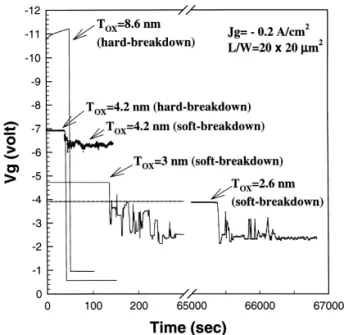
Constant current stressing was employed in this work to explore the time-dependent-dielectric break-down (TDDB) characteristics of ultra-thin oxides. This method is appropriate for characterizing the charging damage since it has been pointed out that the plasma charging is likely to act as a non-ideal current source [17]. Fig. 1 shows typical V±t curves during the measurements with a current density of ÿ0.2 A/cm2.
The abrupt drop in voltage at certain time indicates the occurrence of oxide breakdown. Nevertheless, the magnitude of post-breakdown voltages for SB and HB events are dierent. This dierence has been pointed out in a recent report [18] that the post-breakdown voltage after HB is around 1 V or less, while that after SB can be 1 V in magnitude higher (e.g.>2 V). In ad-dition, the post-SB V±t curves show noisy character-istics. For oxides of 8 nm, only HB was observed, while both SB and HB can be induced in 4 nm-thick oxides, as shown in Fig. 4. When oxide is further scaled to 2.5 nm, it is found that SB exclusively domi-nates the breakdown events. Such a ®nding is also con-sistent with previous results [18], and could be ascribed
Fig. 1. Typical voltage±time curves of charge-to-breakdown measurements.
to the reduced trap generation rate under high ®eld stressing as oxide thickness is reduced.
Fig. 2 shows the eect of stress polarity on the Qbd
results measured at 25 and 1808C, respectively. The de®nition of Qbd used in this work is the amount of
charge reached at the moment when either HB or SB is induced. The magnitude of stressing current density is ®xed at 1 A/cm2. The polarity dependence means the
dierence in Qbdvalues between that obtained by gate
injection (Vg< 0) and substrate injection (Vg> 0). It
has been well documented in previous reports [19, 20] that the polarity dependence increases with decreasing Toxfor oxides thicker than 4 nm, and this is ascribed
to the dierent properties between the poly-Si/oxide and oxide/Si interfaces. In this study, we observe that, as oxide is further scaled down, the polarity depen-dence becomes even stronger at both 258 and 1808C, as shown in Fig. 2. This is mainly due to the rise in Qbd under substrate injection condition as oxide is
thinned down, while the Qbdunder gate injection
stres-sing remains relatively unchanged.
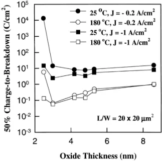
Fig. 3 shows the eects of stress current density and temperature on Qbdunder gate injection stressing. It is
found that Qbd of 2.6 nm-thick oxides is about three
orders of magnitude higher than those of thicker ox-ides under current density of ÿ0.2 A/cm2 (V
ox12.9 V
for Tox= 2.6 nm) at room temperature, indicating the
higher tolerance to high ®eld under DT process. However, when temperature is raised from room
tem-perature to 1808C, Qbd of 2.6 nm-thick oxides
(J =ÿ0.2 A/cm2) is only about one order of magnitude
higher than that of thicker oxides. This implies that the temperature acceleration eect is very signi®cant for ultra-thin oxides under direct tunneling (DT) stres-sing. Such an eect is not clearly understood, and could possibly be related to the properties of oxide/Si interface, since it has been pointed out that the injected electrons may release energy at the interface [21].
By increasing the current density to ÿ1 A/cm2
(Vox13.4 V), the thickness dependence on Qbd shown
in Fig. 3 is not signi®cant at room temperature, while a drop in Qbd is observed at 1808C as Tox is scaled
down. This indicates that, under the F±N stressing, thinner oxides may suer more damage as temperature is raised. In addition, current density dependence of Qbd is also reduced at high temperature. For oxide
thinner than 3 nm, although not as strong as that in DT stressing, the temperature acceleration eect is also very signi®cant. The temperature eect has been reported previously [22, 23]. In this study, however, we ®nd that its role would be even more important as oxide is scaled below 4 nm, thus more attention should be paid in this aspect.
4. Charging damage induced during ashing
In this work, we characterized the charging damage induced in oxides during a photoresist (PR) stripping
step in an RF down-stream O2 plasma asher.
Previously, we have investigated this system and found
Fig. 2. 50% charge-to-breakdown measured at 258 and 1808C as a function of stress polarity and oxide thickness. AAR of the test samples is 4.
Fig. 3. 50% charge-to-breakdown measured at 258 and 1808C under gate injection of ÿ0.2 and ÿ1 A/cm2, respectively, as a
that severe antenna eect could occur at the wafer center [8, 24]. The cause of damage is presumably due to the non-uniform plasma generation resulted from the gas injection mode of the asher [25]. This is
sup-ported by the results of CHARM-2 monitor wafers, which contain a number of EEPROM sensors on the wafer surface used to measure the surface potential developed during plasma processing. Details of the measurement procedure can be found in [26]. As can be seen in Fig. 4(a) and (b), the CHARM-2 sensors recorded large positive and negative potential values at
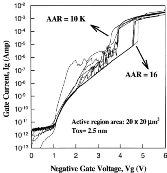
Fig. 5. Current±voltage characteristics of large (AAR = 10,000) and small (AAR = 16) antenna devices with Toxof 4.2 nm.
Fig. 6. Current±voltage characteristics of large (AAR = 10,000) and small (AAR = 16) antenna devices with Toxof 2.5 nm.
Fig. 4. Wafer maps of (a) positive and (b) negative potential values recorded by CHARM-2 sensors.
the wafer edge and center, respectively. In the exper-iments, however, no signi®cant damage was found in devices located at the wafer edge where positive char-ging is incurred. This can be ascribed to the strong po-larity dependence shown in Fig. 2.
Figs. 5 and 6 show typical I±V characteristics of antenna devices with Toxof 4 and 2.5 nm, respectively.
Several devices located at the wafer center with a large AAR of 10,000 were chosen to illustrate the damage
types, while devices with a small AAR of 16 were employed as control samples. In Fig. 5, it is seen that there are basically three types of damage, as rep-resented by types A, B and C, respectively. The former two can be regarded as the SB degradation, since the voltage±time curve under constant current stressing performed on these samples exhibits noisy character-istics similar to that of SB events shown in Fig. 1. The dierence between the two types could be related to the number of SB events already taken place in one sample [12, 13]. Type C represents the HB mode. As Tox is thinned down to 2.5 nm, however, only SB
events appear in large antenna devices, as shown in Fig. 6. This indicates that the oxide degradation pro-cesses could be dierent as oxide is scaled down.
Fig. 7 shows the Qbdas a function of device location
and antenna area ratio for oxides with thickness ran-ging from 2.6 to 8.7 nm. Each datum represents the average result of several measurement sites with identi-cal distance-from-center. Constant current stressing was performed with current density of ÿ0.2 A/cm2.
For ecient characterization, these devices were stressed either to breakdown or to a value of 5000 C/ cm2if the oxides do not fail with stress current density
Fig. 7. Position dependence of charge-to-breakdown (Qbd) as
a function of oxide thickness and antenna area ratio. For samples with 2.6-nm-thick oxide, stress current densities of ÿ0.2 (square symbol) and ÿ1 A/ cm2 (circle symbol) were
used. Qbdvalues are all over 5000 C/cm2for small AAR (16)
samples under ÿ0.2 A/cm2stressing (not shown).
Fig. 8. Charge-to-breakdown results of antenna devices as a function of oxide thickness. The test cells where the large antenna devices (AAR = 10,000) are located are shown in the top portion of the ®gure. Each datum represents the average result of several measurements.
of ÿ0.2 A/cm2. Stressing with ÿ1 A/cm2was also
per-formed on the devices with 2.6 nm-thick oxide. It is noted that the Qbdof devices with small AAR of 16 is
essentially independent of position and, therefore, can indeed be regarded as a damage-free reference, con-®rming our assumption made in previous section. For devices with large AAR (10,000), signi®cant damage begins to appear at the wafer center as oxides are scaled below 6 nm and, for oxides thinner than 4 nm, oxide breakdown is induced at the wafer centre. As oxide is thinned down to 2.6 nm, Qbdhigher than 5000
C/cm2 is observed for samples with small AAR of 16
(not shown) and also for samples with AAR of 10,000, but away from the center region under ÿ0.2 A/cm2
stress condition. In these devices, the abrupt increase in Qbdas compared to that obtained under ÿ1 A/cm2
stress condition is explained by the higher tolerance to tunneling current stressing in DT (ÿ0.2 A/cm2)
pro-cess. Nevertheless, the results shown in Fig. 7(e) clearly indicate that a severe antenna eect is induced at the wafer center.
Oxide thickness dependence on Qbd is illustrated in
Fig. 8, in which the average results obtained from con-trol and damaged (AAR = 10,000) samples are shown and compared. The damaged samples are located in the nine cells (shown in this ®gure) at the wafer center. Constant current stressing of ÿ0.2 A/cm2current
den-sity is performed on these devices. It is seen that, for oxides thicker than 3 nm, Qbd of control samples is
relatively independent of Tox, while that of damage
samples decreases with decreasing Tox. For samples
with Toxof 3 nm, only SB was measured, as indicated
by the `0' value of Qbd in Fig. 8. When Toxis thinned
down to 2.6 nm, Qbd of control devices rises
signi®-cantly due to the transition of stress condition from F±N (Toxe3 nm) to DT process, as mentioned earlier.
Nevertheless, the remaining Qbd measured from the
damage samples is much smaller. From the results shown in Figs. 2 and 3, it is understood that the damage characteristics of thinner oxides are very sensi-tive to stress polarity, current density (or oxide ®eld), and temperature. The antenna eect shown in Figs. 6± 8 can thus be mainly ascribed to the strong negative plasma charging (supported by the results of CHARM-2 monitors shown in Fig. 4), and elevated process temperature (2008C). The latter factor could be
Fig. 9. Threshold voltage, subthreshold swing, and transcon-ductance as a function of cell position. Antenna area ratio of the devices is 20,000. Oxide thickness is 2.5 nm.
Fig. 10. Charge-to-breakdown values as a function of cell pos-ition. Channel length and width of the measured transistor are 1.2 and 10 mm, respectively.
Fig. 11. Gate voltage variation during constant current stres-sing for devices located at the wafer center with small (AAR = 500) and large (AAR = 20,000) antenna.
even more important since the associated acceleration eect is very signi®cant under both F±N and DT char-ging stress conditions.
The above analysis is mainly based on the Qbd
characterization. When other indicators are used, the feature of outcome might be dierent. This is shown in Fig. 9, in which Vth, subthreshold swing (SS), and
transconductance (Gm) of transistors with Tox of
2.5 nm and AAR of 20,000 are plotted as a function of device location. There seems to be no degradation in this plot. However, when Qbd is used to characterize
these devices, as shown in Fig. 10, signi®cant antenna eect is identi®ed. Such ®nding is ascribed to the
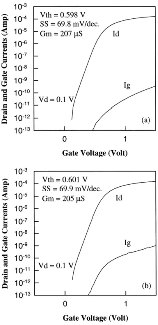
sig-ni®cant decrease in the rates of trap creation and inter-face state generation under high-®eld stressing as oxide is scaled down (see Fig. 1) [20]. It is noted that the breakdown events found in the measurements of Fig. 10 all belong to the soft-breakdown type, consist-ent with the ®ndings shown previously [18] and in the previous section. Typical Vg±t curves during constant
current stressing are illustrated in Fig. 11. It is seen that soft breakdown with noisy characteristics [18] appears for large antenna device from the beginning of stressing. Interestingly, subthreshold characteristics of a transistor with such thin oxide depict little changes even after the charge-to-breakdown test. An example is shown in Fig. 12, in which the Vth, SS and Gmremain
almost unchanged after oxide is stressed to
soft-break-down. Similar results were also reported
recently [18, 27]. The only parameter that depicts sig-ni®cant change shown in the ®gures is the gate leakage (Ig), which increases signi®cantly after oxide
break-down. This could explain the dierent outcomes between Figs. 9 and 10 in monitoring the antenna eect.
5. Discussion and conclusions
Eects of gate oxide scaling on the plasma charging damage could be very complicated based on results obtained in this work. First of all, the occurrence of SB failure mode in the ultra-thin oxide regime has cer-tain impacts on the device degradation caused by plasma charging. Even though the increase in gate leakage after SB does not exceed the drain current, and thus may not signi®cantly aect the I±V character-istics of a transistor, it does impose certain concerns on circuit applications, such as the power consump-tion, data retention characteristics of memory devices, as well as the noise performance.
Regarding the plasma process conditions, three im-portant factors should be carefully considered, namely, plasma current density, charging polarity and wafer temperature during processing. Among them, poten-tially enhanced damage eect caused by high plasma current presents an emerging concern, since more and more HDP tools are being implemented in modern production lines. The magnitude of charging current the antenna devices may encounter in an HDP en-vironment could be of the order of 10 A/cm2 [28],
which is two orders higher than that in a conventional diode reactor. Such high current level would aggres-sively damage ultra-thin oxides in a short period.
It is also shown that the stress polarity dependence increases with decreasing oxide thickness down to 2.5 nm. This indicates that negative plasma charging may produce far more severe damage than positive plasma charging as oxide is thinned down, as is
evi-Fig. 12. Drain and gate currents as a function of gate voltage measured (a) before and (b) after charge-to-breakdown test. Channel length and width of the measured transistor are 1.2 and 10 mm, respectively.
denced by the experimental results. Consequently, more attention should be paid on the regions of wafer surface where negative charging is identi®ed.
The temperature acceleration eect is very signi®cant for ultra-thin oxides. It is noted that any conclusion based on the extrapolation of Qbdmay not be reliable.
In fact, one of the main purposes of this paper is to emphasize the accelerated degradation under high tem-perature and high stressing current, thus extrapolation would be unreliable. However, in this paper we also emphasize that these high-temperature, high-stressing current conditions do occur in real wafer processing steps (such as ashing and CVD), and therefore careful attention should be paid to ensure the resultant gate oxide integrity.
Finally, we have also compared the usefulness of several indicators in revealing the antenna eect. It is found that traditional methods of monitoring transis-tor parameters, including Vth, SS and Gm, may not be
appropriate for detecting the charging damage in ultra-thin gate oxides. Consequently, some destructive methods, such as the charge-to-breakdown measure-ment, or the noise characterization techniques [9, 18], are necessary to evaluate plasma damage in ultra-thin oxides.
Acknowledgements
The authors would like to thank the sta of National Nano Device Laboratories and Dr B. Y. Tsui (ITRI/ERSO) for their technical assistance during the course. This work was supported by National Science Council of the Republic of China under contract no. NSC-87-2721-2317-200.
References
[1] Shone F, Wu K, Shaw J, Hokelek E, Mittal S, Haranahalli A. Symp VLSI Technol Dig Tech, 1989. p. 73±74.
[2] Wu IW, Koyanaki M, Holland S, Huang TY, Bruce RH, Anderson GB, Chiang A. J Electrochem Soc 1989;136:1638±44.
[3] Park D, Hu C. International Symposium on Plasma Process-Induced Damage (P2ID), 1997;15.
[4] Alavi M, Jacobs S, Ahmed S, Chern CH, McGregor P. International Symposium on Plasma Process-Induced Damage (P2ID), 1997:7±10.
[5] Noguchi K, Tokashiki K, Horiuchi T, Miyamoto H. IEDM Tech Dig 1997;441±444.
[6] Bayoumi A, Ma S, Langley B, Cox M, Tavassoli M, Diaz C, Cao M, Marcoux P, Ray G, Greene W. International Symposium on Plasma Process-Induced Damage (P2ID), 1997;11.
[7] Krishnan S, Dostalik WW, Brennan K, Aur S. IEDM Tech Dig 1996;731±734.
[8] Chien CH, Chang CY, Lin HC, Chang HF, Chiou SG, Chen LP, Huang TY. IEEE Electron Device Lett 1997;18:33±5.
[9] Krishnan S, Rangan S, Hattangaty S, Xing G, Bernnan K, Rodder M, Ashok S. IEDM Tech Dig 1977;445±448. [10] Soloman P. J Vac Sci Technol 1977;14;1122±1128. [11] Jackson JC et al. Appl Phys Lett 1997;71:3682±4. [12] Okada K, Kawasaki S, Hirofuji Y. Extended Abstracts
of Solid State Device and Materials (SSDM), 1994. p. 565±568.
[13] Lee SH, Cho BJ, Kim JC, Choi SH. IEDM Tech Dig, 1994. p. 605±608.
[14] Schuegraf KF, King CC, Hu C. Ultra-thin silicon diox-ide leakage current and scaling limit. In: Symp VLSI Technol Dig Tech, 1992. p. 18±19.
[15] Chen K, Hu C, Fang P, Gupta A. IEEE Electron Device Lett 1997;18:275±7.
[16] Lin HC, Wang MF, Chen CC, Hsein SK, Chien CH, Huang TY, Chang CY, Chao TS. Proceedings of IRPS, 1998. p. 312±317.
[17] Shin H, Nokuchi K, Hu C. Proceedings of IRPS, 1993. p. 272±279.
[18] Weir BE, Silverman PJ, Monroe D, Krisch KS, Alam MA, Alers GB, Sorsch TW, Timp GL, Baumann F, Liu CT, Ma Y, Huang D. IEDM Tech Dig 1997;73(76). [19] Hokari Y. IEEE Trans Electron Device 1988;35:1299±
307.
[20] Han LK, Bhat M, Wristers D, Fulford J, Kwong DL. IEDM Tech Dig 1994;617±620.
[21] Schuegraf KF, Hu C. IEDM Tech Dig 1994;609±612. [22] Ma S, McVittie JP, Saraswat KC. IEEE Electron Device
Lett 1997;16:534±6.
[23] Brozek T, Chan YD, Viswanathan CR. IEEE Electron Device Lett 1996;17:288±90.
[24] Lin HC, Chien CH, Wang MF, Huang TY, Chang CY. International Symposium on Plasma Process-Induced Damage (P2ID), 1997:247±250.
[25] Fang S, McVittie JP. IEEE Trans Electron Devices 1997;41:1034±42.
[26] Lukaszek W, Birrell AH. International Symposium on Plasma Process-Induced Damage (P2ID), 1995;30. [27] Lin HC, Chen CC, Wang MF, Chien CH, Hsein SK,
Chao TS, Huang TY, Chang CY. IEEE Electron Device Lett 1998;19:68±70.
[28] Cheung KP, Liu CT, Chang CP, Pai CS. International Symposium on Plasma Process-Induced Damage (P2ID), 1998;34.