Polymer space-charge-limited transistor
Yu-Chiang Chao, Hsin-Fei Meng, and Sheng-Fu Horng
Citation: Applied Physics Letters 88, 223510 (2006); doi: 10.1063/1.2207838
View online: http://dx.doi.org/10.1063/1.2207838
View Table of Contents: http://scitation.aip.org/content/aip/journal/apl/88/22?ver=pdfcov Published by the AIP Publishing
Articles you may be interested in
High output current in vertical polymer space-charge-limited transistor induced by self-assembled monolayer Appl. Phys. Lett. 101, 093307 (2012); 10.1063/1.4748284
High-performance space-charge-limited transistors with well-ordered nanoporous aluminum base electrode Appl. Phys. Lett. 99, 093306 (2011); 10.1063/1.3632045
Space-charge limited conduction in doped polypyrrole devices J. Appl. Phys. 107, 093716 (2010); 10.1063/1.3373393 Light-emitting polymer space-charge-limited transistor Appl. Phys. Lett. 93, 223301 (2008); 10.1063/1.3027057 Space-charge-limited bipolar currents in polymer / C 60 diodes J. Appl. Phys. 92, 5575 (2002); 10.1063/1.1509839
This article is copyrighted as indicated in the article. Reuse of AIP content is subject to the terms at: http://scitation.aip.org/termsconditions. Downloaded to IP: 140.113.38.11 On: Wed, 30 Apr 2014 08:24:41
Polymer space-charge-limited transistor
Yu-Chiang Chao and Hsin-Fei Menga兲
Institute of Physics, National Chiao Tung University, Hsinchu, Taiwan 300, Republic of China
Sheng-Fu Horng
Department of Electric Engineering, National Tsing Hua University, Hsinchu, Taiwan 300, Republic of China
共Received 15 March 2006; accepted 1 May 2006; published online 2 June 2006兲
A metal grid is sandwiched between poly共3-hexylthiophene兲 to form a solid-state version of vacuum tube triode, where the vertical space-charge-limited current is modulated by the grid potential. The Al grid contains random submicron openings formed by a nonlithographic method. The multilayer polymer structure is made by spin coating. The operating voltage of the polymer space-charge-limited transistor is 3 V, and the current gain of 506 is obtained. The characteristics of the transistor can be tuned by the diameters and the density of the openings on the grid. Similar to the vacuum tube triode, the current follows a power law voltage dependence. © 2006 American
Institute of Physics. 关DOI:10.1063/1.2207838兴
Electronic devices based on organic semiconductors pro-vide attractive alternatives to inorganic devices due to their lower cost as well as the compatibility with flexible sub-strates. One of the key components in the organic electronic circuits is the polymer field-effect transistor共FET兲.1,2Many researches on polymer FET have demonstrated reasonable performance3,4and the possibility of integration with organic light-emitting diodes.4–7Current polymer field-effect transis-tors are mostly horizontal ones in which source and drain electrodes lie in the same plane of the substrate. Due to the intrinsically low carrier mobility in conjugated polymers relative to inorganic semiconductors and the expensive li-thography process for reducing the channel lengths to the submicron, some research efforts were made on the vertical type FET in which the channel length is defined by the thick-ness of the insulating layer vertically separating the drain and source electrodes.8–10 However, so far most techniques uti-lized in vertical-channel organic FETs do not take advan-tages of the low-cost and large-area solution process unique to conjugated polymers.
To circumvent the limits of both horizontal and vertical FETs, vertical non-field-effect organic transistors with multilayer structures were reported.11–18In these devices the channel length is defined by the total thickness of the organic layer and the current is modulated by a highly conductive layer embedded in the organic material. One example is the organic static-induced transistor 共SIT兲 with a striped metal layer embedded in the thermally evaporated organic layer.14,16 It has a similar structure with the vacuum tube triode, which consists of the cathode for electron emissions by heating, the anode for electron collection, and the grid for current modulation. In a vacuum tube triode both the grid and anode electrodes are able to control the potential within the device but the grid is much more effective in controlling the gradient near the cathode. When the grid is in large and negative bias, the electrons experience a negative gradient of potential after they are emitted from cathode. Effectively the electrons encounter a large energy barrier between cathode and anode, and consequently very few of them can be
col-lected by the anode. On the contrary, if the grid is slightly negative biased or positively biased, it is possible for the electrons to find a passage through the potential minimum between two grid wires. Despite similar structure, in SIT the current is modulated by a junction potential barrier while in vacuum tube triode the space-charge-limited current共SCLC兲 is modulated.19
In 1952 Schockley proposed the “analog transistors” as the first solid-state device whose operation resembles that in the vacuum tube triode with current limited by the SCLC.20 While SCLC is not the most common mode of transport in high-mobility inorganic semiconductors, in organic semicon-ductors it is well known that the current is governed by SCLC. Therefore, conjugated polymer might be one candi-date for the vertical non-FET analog transistor.17,18 In this letter we present a vertical polymer version of solid-state vacuum tube triode with an embedded metal grid. A more transparent name “space-charge-limited transistor” is given to this device. The metal grid made of Al film with random openings functions similarly to the grid in vacuum tube tri-ode. The fabrication processes of polymer space-charge-limited transistor have both the advantages of short channel length and easy large-area solution processes. The carriers in the transistor are injected from the emitter, going through the openings on the metal grid and finally arriving at the collec-tor. The potential distribution between emitter and collector can be controlled by the voltages of grid and collector. When the voltages of the grid and collector constitute a high barrier between the emitter and the opening, few carriers can arrive at the collector through the openings. On the other hand, if there is no barrier the carriers can go through the opening and reach the collector. The magnitude of the collector cur-rent is determined by the SCLC given by the potential dif-ference between the emitter and the center of the opening. Collector current is modulated by the grid which controls the effective potential at the opening for fixed emitter and col-lector potentials.
The multilayer structure of the polymer space-charge-limited transistor is indium tin oxide 共ITO兲 glass/ PEDOT:PSS/P3HT/Al grid/P3HT/Al, as shown in Fig. 1共a兲. P3HT is poly共3-hexylthiophene兲 which is used as the semi-conducting polymer between the electrodes. PEDOT:PSS is poly共3,4-ethylenedioxythiophene兲 doped with polystyrene a兲Author to whom correspondence should be addressed; electronic mail:
APPLIED PHYSICS LETTERS 88, 223510共2006兲
0003-6951/2006/88共22兲/223510/3/$23.00 88, 223510-1 © 2006 American Institute of Physics
This article is copyrighted as indicated in the article. Reuse of AIP content is subject to the terms at: http://scitation.aip.org/termsconditions. Downloaded to IP: 140.113.38.11 On: Wed, 30 Apr 2014 08:24:41
sulfonated acid. PEDOT:PSS with a work function of 5.2 eV serves as an Ohmic contact for hole injection into the highest occupied molecular orbital共HOMO兲 of P3HT at 5.1 eV. The injected holes can pass through the openings on Al grid and finally arrive at Al collector as the transistor is on. The low-est unoccupied molecular orbital共LUMO兲 of P3HT is 3 eV, which is 1.3 eV higher than the Al work function of 4.3 eV to suppress unwanted electron current from Al to P3HT. Two differences between vacuum tube triode and the present polymer space-charge-limited transistor shall be mentioned. First, the carrier is hole in polymer space-charge-limited transistor while the carrier is electron in vacuum tube triode. Second, the carrier injection in polymer space-charge-limited transistor is via Ohmic contact, while in vacuum tube triode it is via thermionic emission of heated cathode. The basic operation principle of the transistor is illustrated in Fig. 1共b兲. The dotted line is the potential profile along a path passing through the metal grid, while the dash line is the profile along a path through the opening. As the transistor is off, no hole is collected due to the barrier between the emitter and opening. As the transistor is on, there is a SCLC between the emitter and opening.
The device is fabricated on patterned ITO glass substrate cleaned in ultrasonic bath. A layer of 500 Å PEDOT:PSS is spin coated onto ITO as the hole injection layer. After baking in vacuum at 200 ° C for 10 min, the substrate is transferred to a glove box. P3HT is spin coated from chloroform solu-tion 共1 wt %兲 on the PEDOT:PSS layer, and then baked at 120 ° C for 30 min in vacuum. A spin rinsing21,22with xylene is used to remove the remaining soluble part of P3HT, and a thin P3HT layer of about 200 Å is obtained. To fabricate Al grid with openings, polystyrene spheres are used as shadow mask. Ethanol solution 共0.1 wt %兲 of polystyrene spheres with various diameters is spin coated on P3HT, followed by 300 Å Al evaporated as the Al grid. After removing the poly-styrene spheres by submerging the sample in ethanol for 20 s with ultrasonic agitation, an Al film with openings at the positions of the spheres is formed. A layer of 450 Å P3HT is then spin coated from xylene solution 共1 wt %兲 on the sample, followed by depositing an Al film of 300 Å to com-plete the device. Ethanol was used to dilute the polystyrene spheres because its alkyl group improves the adhesion be-tween polymer and polystyrene solution. The device active area is 1 mm2.
The AFM images of the surface of Al grid after removal of polystyrene spheres of 2000 and 5000 Å are shown in Figs. 2共a兲 and 2共b兲, respectively. The sizes of the openings are almost identical to the diameter of polystyrene spheres, which are removed without causing mechanical damages to the Al grid and the underlying spin-rinsed P3HT film. The spin-rinsed P3HT is intended to provide three advantages. First, the thickness of spin-rinsed P3HT film is usually less than 200 Å, which makes the Al grid much closer to the emitter than the collector. This geometry, similar to the vacuum tube triode, facilitates the Al grid to easily control the potential distribution near the emitter. Second, after the P3HT is spin rinsed with xylene, the film is not easy to be dissolved by xylene in the subsequent processes. This does not only prevent the possible dissolution when spin coating P3HT from xylene on Al grid but also the possible shorting between the emitter and Al grid caused by deformation. Third, the spin-rinsed P3HT film is robust during the re-moval of polystyrene spheres by ultrasonic agitation.
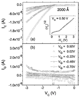
Figure 3共a兲 shows the characteristics of polymer space-charge-limited transistor with hole diameter of 2000 Å on Al grid. ICand VCare the collector current and voltage, respec-tively. The ITO electrode is commonly grounded and the Al collector is negatively biased at VCwith respect to ITO. The negative ICmeans that holes are driven toward the collector through the grid. The IChas apparent modulation by the grid voltage VG. As shown in Fig. 3共b兲, the grid current IGis in the order of 10−10A when different V
Gare applied. To avoid FIG. 1. 共Color online兲 共a兲 Device structure of the polymer
space-charge-limited transistor.共b兲 The potential profile for the on and off states of the transistor. The dash line is along the channel through the grid opening, while the dotted line is along the grid electrode. The solid line is the Fermi level of Al and PEDOT.
FIG. 2. 共Color online兲 The AFM images of the Al grid after removal of polystyrene spheres with diameter of共a兲 2000 Å and 共b兲 5000 Å. Note the aggregate at the upper right corner of共a兲.
FIG. 3. 共a兲 Collector current IC and共b兲 grid current IGas a function of
collector voltage VCat different grid bias VGof device with 2000 Å
open-ings on Al grid.
223510-2 Chao, Meng, and Horng Appl. Phys. Lett. 88, 223510共2006兲
This article is copyrighted as indicated in the article. Reuse of AIP content is subject to the terms at: http://scitation.aip.org/termsconditions. Downloaded to IP: 140.113.38.11 On: Wed, 30 Apr 2014 08:24:41
large IG, VG is restricted to be not more negative than −0.85 V which is the built-in potential between PEDOT:PSS and Al. A large IG is obtained when negative VGis applied beyond −0.9 V. The current gain, defined by dIC/ dIG, is 506 when VC is −3 V. The transconductance gm=共dIC/ dVG兲 is 3.21⫻10−6S, calculated from the slope of the I
C-VG curve in the range from −0.75 to − 0.81 V. The off current can be reduced by continuing to increase VGuntil the occurrence of a large leakage current between the grid and collector. In principle, lower off current can be achieved by reducing the aggregate of polystyrene spheres, which introduce the big holes on the Al grid film shown in the upper right corner of Fig. 2共a兲. In order to verify the presumption that this device works in the same way as in vacuum tube triode, we look for signature of the SCLC behavior. The collector current for the vacuum tube triode is given by IC= C共VG+ VC兲n. is the grid amplification factor.19 The linear combination of grid and collector potentialVG+ VC is the effective potential at the opening. n = 3 / 2 for ballistic SCLC in vacuum and n = 2 for diffusive SCLC in solid state. Plotting IC1/2against VCin the inset of Fig. 3共a兲 indeed gives a straight line once the barrier at the opening is supressed, confirming the key SCLC presumption. For SIT, IC would depend exponentially on
VC.19
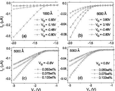
The diameter and density of the openings are also crucial to the properties of polymer space-charge-limited transistor. As demonstrated in Fig. 4共a兲, the IC-VCcurves of the device with opening diameter of 1000 Å are overlapped with posi-tive VG. On the other hand, curves corresponding to the de-vice with opening diameter of 5000 Å separate from each other but with a high off current. The current is difficult to be turned off because of the region around the center of the opening is too far from the Al grid, thus the potential barrier is only enhanced slightly by grid potential共Ⰶ1兲 before the leakage current between the reverse-biased grid and collector occurrs. Therefore the optimal opening diameter falls in the range of 1000 and 5000 Å. Figures 4共c兲 and 4共d兲 show the
characteristics of polymer space-charge-limited transistor with different opening density when VGis −0.8 and 0.8 V. Higher IC is obtained with higher concentration of polysty-rene sphere solution in the fabrication process of Al grid. This indicates that by using the higher concentration of poly-styrene sphere solution the higher opening density is ob-tained, which in turn leads to more current paths and higher
IC. The way to achieve high polystyrene sphere density with-out aggregation like the case shown in Fig. 2共a兲 will be the key issue for further study.
In summary, a solution-processed vertical polymer space-charge-limited transistor is demonstrated. A nonlitho-graphic method is introduced for Al grid fabrication with different opening diameters. The operating voltage is as low as 3 V. The transconductance is 3.21⫻10−6S and the cur-rent gain is 506. Such device concept has the potential ad-vantages of easy large-area solution process, high current, low voltage, and being lithography-free.
This work is supported by the National Science Council of Taiwan of the Republic of China and the Excellence Project of the ROC Ministry of Education.
1B. Crone, A. Dodabalapur, Y.-Y. Lin, R. W. Filas, Z. Bao, A. LaDuca, R. Sarpeshkar, H. E. Katz, and W. Li, Nature共London兲 403, 521 共2000兲. 2L. L. Chua, R. H. Friend, and P. K. H. Ho, Appl. Phys. Lett. 87, 253512
共2005兲.
3J. Park, S. Y. Park, S.-O. Shim, H. Kang, and H. H. Lee, Appl. Phys. Lett.
85, 3283共2004兲.
4H. Sirringhaus, N. Tessler, and R. H. Friend, Science 280, 1741共1998兲. 5A. Dodabalapur, Z. Bao, A. Makhija, J. G. Laquindanum, V. R. Raju, Y.
Feng, H. E. Katz, and J. Rogers, Appl. Phys. Lett. 73, 142共1998兲. 6K. L. Tzeng, H. F. Meng, M. F. Tzeng, Y. S. Chen, C. H. Liu, S. F. Horng,
Y. Z. Yang, S. M. Chang, C. S. Hsu, and C. C. Chi, Appl. Phys. Lett. 84, 619共2004兲.
7Z. L. Li, S. C. Yang, H. F. Meng, Y. S. Chen, Y. Z. Yang, C. H. Liu, S. F. Horng, C. S. Hsu, L. C. Chen, J. P. Hu, and R. H. Lee, Appl. Phys. Lett.
84, 3558共2004兲.
8N. Stutzmann, R. H. Friend, and H. Sirringhaus, Science 299, 1881 共2003兲.
9R. Parashkov, E. Becker, G. Ginev, T. Riedl, M. Brandes, H.-H. Johannes, and W. Kowalsky, Appl. Phys. Lett. 85, 5751共2004兲.
10R. Parashkov, E. Becker, S. Hartmann, G. Ginev, D. Schneider, H. Krau-twald, T. Dobbertin, D. Metzdorf, F. Brunetti, C. Schildknecht, A. Kam-moun, M. Brandes, T. Riedl, H.-H. Johannes, and W. Kowalsky, Appl. Phys. Lett. 82, 4579共2003兲.
11S. Fujimoto, K. Nakayama, and M. Yokoyama, Appl. Phys. Lett. 87, 133503共2005兲.
12Y. C. Chao, S. L. Yang, H. F. Meng, and S. F. Horng, Appl. Phys. Lett. 87, 253508共2005兲.
13M. S. Meruvia, A. R. V. Benvenho, I. A. Hümmelgen, A. A. Pasa, and W. Schwarzacher, Appl. Phys. Lett. 86, 263504共2005兲.
14Y. Watanabe and K. Kudo, Appl. Phys. Lett. 87, 223505共2005兲. 15L. P. Ma and Y. Yang, Appl. Phys. Lett. 85, 5084共2004兲.
16K. Kudo, S. Tanaka, M. Iizuka, and M. Nakamura, Thin Solid Films 438, 330共2003兲.
17J. McElvain, M. Keshavarz, H. Wang, F. Wudl, and A. J. Heeger, J. Appl. Phys. 81, 6468共1997兲.
18Y. Yang and A. J. Heeger, Nature共London兲 372, 344 共1994兲.
19K. N. Kwok, Complete Guide to Semiconductor Devices, 2nd ed.共Wiley, New York, 2002兲.
20W. Shockley, Proc. IRE 40, 1289共1952兲.
21J. S. Kim, R. H. Friend, I. Grizzi, and J. H. Burroughes, Appl. Phys. Lett.
87, 023506共2005兲.
22S. A. Choulis, V.-E. Choong, M. K. Mathai, and F. So, Appl. Phys. Lett.
87, 113503共2005兲.
FIG. 4. The characteristics of the polymer space-charge-limited transistor with共a兲 1000 Å and 共b兲 5000 Å opening diameter on Al grid. The charac-teristics of the polymer space-charge-limited transistor with different con-centration of polystyrene spheres used in fabrication process when VGis共c兲
−0.8 V and共d兲 0.8 V.
223510-3 Chao, Meng, and Horng Appl. Phys. Lett. 88, 223510共2006兲
This article is copyrighted as indicated in the article. Reuse of AIP content is subject to the terms at: http://scitation.aip.org/termsconditions. Downloaded to IP: 140.113.38.11 On: Wed, 30 Apr 2014 08:24:41