Graph-based Wire Planning for Analog Circuits
Abstract―In this paper, we propose the graph-based
approach which constructs the electromigration-free wire planning according to the current characteristics of sources and sinks. The objective of this paper is to minimize the total wiring area of the wire planning without electromigration, i.e. enhance the mean time before failure. First, we construct the complete bipartite graph which the weight of each edge is with consideration of distance between each source-sink pair and current capacity for all sources and sinks. Second, we sort the weights of all edges with the ascending order. Third, the edge with the minimal current-distance weight is selected to remove from the complete bipartite graph. Furthermore, we iteratively update the supply current of the current source and the weights of the corresponding edges which are connected to the current source. Finally, the greedy method terminates until the current capacity of all sources are zero. Five benchmark circuits are used to evaluate the proposed algorithm and experimental results show that the proposed approach efficiently gets the better solution and effectively minimizes the wiring area with consideration of electromigration.
Index Terms― Electro migration, space reservation,
Wire Planning, Obstacle-avoiding routing, Graph theory.
I. INTRODUCTION
Automation of analog circuit is getting more and more important. Traditionally, the analog circuit is designed by using the manually because there are huge experiences to produce the analog circuit with the high performance and the better circuit characteristics. Nowadays, some researches focus on the circuit automation [7][8] such as the placement of summitry, parameters determination by mathematical programming, automation wire planning to enhance circuit reliability [9].
A. Previous works about wire planning
Automation of wire planning plays an important role on the circuit reliability. Lienig et al. introduced the physical design flow which
integrates current-driven planning and verification and presented a concept to assign the large current value to the short path with consideration of electromigration. [8]. Jerke et al. presented the post-routed approach to modify the critical layout structures to increase the reliability and reduce the number of violations [3]. Lienig et al. proposed a new approach, which effectively determines all wires width in the given terminals [14]. Furthermore, their approach is verified by using a real world analog design. Adler et al. presented a single layer router, which satisfies the current constraints and the maximum current density for all interconnect [1]. Adler et al. proposed a new greedy-based approach, which determines the wire width for a multi-terminal net with consideration of the obstacles, to solve the current-driven routing problem [2]. With consideration of the obstacles, their approach can find the proper routing path according to the wire width and the available routing space between the adjacent obstacles. Lienig et al. provided two approaches to handle the analog multiple terminals net while satisfying the Kirchoff’s current law [14]. Besides, they discussed the concept of the over-sizing for the arbitrary polygon. Lienig et al. proposed an analog router, which handle non-rectangular obstacles with the non-Manhattan-based routing, for the current- driven routing [15][16]. Yan et al. propose the greedy-based method to minimize the total wiring area to satisfy Kirchoff’s current law without the obstacles [18]. Most of them can not obtain the optimal current-driven wire planning.
B. Previous works about obstacle-avoiding routing
Many routing algorithms are presented to minimize the total wirelength with obstacles. Chiang et al. [6] proposed the octilinear Steiner tree algorithm by using the edge-conversion and
Tsai-Ming Hsieh
Dept. of Info. and Computer Engineering Chung Yuan Christian University,
Chung-Li, Taiwan, R.O.C. hsieh@cycu.edu.tw Cheng-Chiang Lin
Dept. of Info. and Computer Engineering Chung Yuan Christian University,
Chung-Li, Taiwan, R.O.C. matrix_lin2002@yahoo.com
Pei-Shan Wu, Jiun-Ying Yu, Yu-Cheng Lin
Dept. of Info. and Electronic Commerce
Kainan University, Taoyuan, Taiwan, R.O.C.
linyu@mail.knu.edu.tw
Hsin-Hsiung Huang Dept. of Electronic Engineering
Lunghwa Univ. of Science and Technology,
Steiner-sliding approaches. Ho et al. [10] provided the X-arch Steiner tree algorithm to use the Delaunay triangulation to cluster terminals and sort total length of each three-terminal to generate the optimal connection. Shen et al. [17] proposed a graph-based method which first constructs a graph by the terminals and obstacles, finds the minimal spanning tree from the connection graph and construct the rectilinear Steiner tree. However, most of them deal with the digital circuit without consideration of the circuit characteristics of analogy circuits.
C. Contribution of our works
The contributions of this work are as follows. First, to avoid the electormigration of the circuit, the greedy-based approach, which formulates the problem into the graph model, is used to automatically determine the feasible connections between sources and targets with the proper wire width. Second, to avoid the interference between the obstacle and wires, the space reservation [5][11] is utilized for all obstacles. Third, the proposed method, which computes the obstacle-avoiding length by using the push_line method, efficiently determines the routing path to reduce the total wiring area with the current capacities of all sources and sinks.
D. Outline of the proposed work
The rest of the paper is as follows. Section II describes the terminology and the problem formulations. The Section III discusses the proposed algorithm with an example in detail. The experimental results and conclusions are attached in Sections IV and V, respectively.
II.PRELIMINARY
In the section, we first discuss the terminology and then define the problem formulation. In the paper, the Manhattan-architecture which supports the vertical and horizontal segments for the routing is applied to connect for the sources and sinks with consideration of the current capacity.
A. Terminology
First, the wirelngth with consideration of obstacles is discussed. With consideration of the obstacle penalty, the wire length due to the obstacles [12][17] is involved in the cost function. For each connection between sourcesi=( ,x yi i) and targettj=( ,x yj j), the obstacle-avoiding Manhattan length is estimated as follows,
( , ) | i j| | i j | min( u( , ), l( , ))
d i j = x −x + y −y + len i j len i j (1)
where len i ju( , ) and len i jl( , ) denote the additional obstacle-avoiding wire lengths of the upper-L and low-L routing paths, respectively.
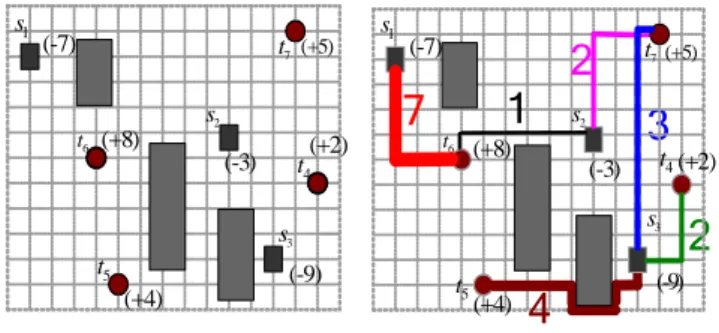
1 s 6 t 5 t 3 s 4 t 2 s 7 t ( 5)+ (-7) ( 8)+ ( 4)+ (-9) ( 2)+ (-3)
2
3
1 s 6 t 5 t 3 s 4 t 2 s 7 t7
1
4
2
( 5)+ (-7) ( 8)+ ( 4)+ (-9) ( 2)+ (-3) (a) Original circuit (b) resultsFigure 1. Illustration of wire planning.
Second, we illustrate the formula to compute the total wiring area. The wiring area of the current-driven wire planning is defined by,
, A ( , ) ( , ) i j c i j d i j α =
∑
× × (2) where A is the total wiring area of the certain wire planning. c i j and ( , ) d i j are the capacity and ( , ) distance for source i and sink jFor Figure 1(a), the wiring area of the wire planning obtained by the heuristic algorithm proposed by [18]. In the paper, the graph-based method is proposed to solve the problem of wiring planning with the obstacles. The additional wirelength due to the obstacles could be taken into
account by using our proposed method. With the obstacles, the total the wiring area of current-driven M-arch wire planning by the
7 7 1 7× + × + × + × + × + ×2 7 3 10 2 5 4 10=150 (3)
Above discussion show the formula to compute
the total wiring area for the M-arch wire planning.
B. Problem Definition
For the copper or aluminum interconnect the electromigration result in open or short if the wire width is not sufficient. To increase the reliability of the interconnect with the minimization of wiring area, we should assign the minimal wire width according to the current density among the sources and targets. We propose the current-driven routing algorithm which automatically determines the wire widths for all wires with obstacles. Therefore, we define the problem as follows,
Given a net N containing a set of sources
1 2
{ , ,..., }n
S= s s s and a set of
targets T ={ , ,..., }t t1 2 tm with their corresponding
root-mean-square current values {O O1, 2,...,On}
and{ ,I I1 2,..., I }m , respectively. Besides, there is a set
of obstacles B={ ,b b1 2,...,bk}in the analog circuit.
The objective is to construct an X-arch wire planning with minimal wiring area with consideration of the obstacles and Krichhoff’s current laws [3][4].
III.THE GRAPH-BASED WIRE PLANNING In this section, the graph-based greedy method is proposed to perform the wire planning to minimize the total wiring area. Four steps of the algorithm are first discussed and an example is used to illustrate the operation.
A. Description of greedy graph-based method
First, we construct the bipartite graph according to the relationship of all sources and all sinks. The noise idea which is inversely proportional to the distance between adjacent wires is proposed in [19][20]. To avoid the interference between the obstacle and interconnections, we reserve the dead-space along the obstacle.
original obstacle
virtual obstacle
wire
Figure 2. Avoid the interference
The weights of all edges in the complete bipartite graph are assigned by the formula,
( , ) ( , )
w i j = ×α d i j (4) where d i j are the distance for source i and sink ( , )
j, respectively. Besides,α is the ratio between the
current capacity and the assigned wire width. To reduce the total wiring area with consideration of electromigration, the proper wire width is determined according to the information of the bipartite graph.
Second, we sort the weights of all edges with the ascending order. We first deal with the edge with minimization product of distance and current capacity. It means that the edge with the current minimal weight is selected to remove from the complete bipartite graph.
Third, we update the supply current of the current source and the weights of the corresponding edges which are connected to the current source. Of course, we should check if the total current capacities of all sources are equal to the total current of all sinks.
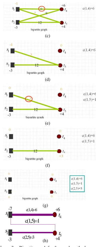
1
s
4t
5t
2s
-7
-3
+6
+4
c(1,5)=1
c(1,4)=6 c(2,5)=3 1s
4t
5t
2s
-7 -3 +6 +4Finally, the greedy method terminates until the current capacity of all sources are zero. In other words, the total driving current of all sources is equal to the total sinking current of all sinks.
B. Example to illustrate the operation
We take the following example to illustrate the concept of the graph-based method. Figure 3(a) and (b) denote the original circuit with two sources (black squares) and two sinks (dotted circles) and the complete bipartite graph. Figure 3(c) is the results when we select the edge with 6 current values. The current value of source 1 is update to “-1” (i.e. -7+6). The corresponding results are shown in Figure 3(d) after removing a edge for the complete bipartite graph. Figure 3(e) and (f) are the results when we iterative update the current for the sources and remove the other edge for the complete bipartite graph. Finally, we observe the total currents of the source are all assigned to all sinks by the graph-based method, see Figure 3(g) and (h). (a) (b) (c) (d) (e) (f) (g) (h)
IV.EXPERIMENTAL RESULTS
Our greedy graph-based approach is implemented by using C++ language on an Intel Core2 Duo 1.87G and 1.86G machine having 3GB main memory. The objective of the problem is to minimize the total wiring area of the current-driven wire planning with Kirchhoff’s law. Because we are lack of the benchmarks and source codes in [8][9][10][11], the different benchmarks, which contain the sources, targets and obstacles, are modified from papers. The minimal wire width set to be 1um. Because of the lack of the real data, the RMS current values of sources and targets are randomly determined within the user-defined range. Obviously, our graph approach reduces the wiring area with the obstacles. For all benchmark, the statistics such as the number of obstacles, terminals, sources, targets are shown in Table 1.
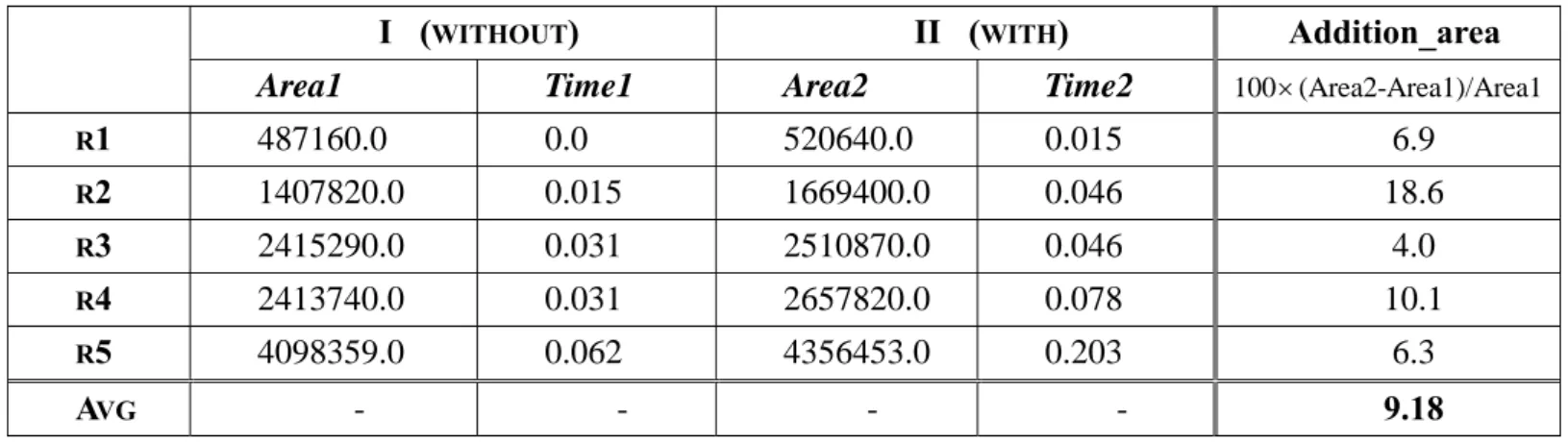
First, we explore the effective of our graph-based method for improvement on the total wiring area without and with the obstacles. The obstacle ratios of the chip are from 8.2 to 39.4%. To deserve to be mentioned, the huge ratio of obstacles appears in R5. But the additional wiring area is only 4%. In Table 2, compared to the results without obstacles, we observe that the additional total wiring area with obstacles is increased only 9.18% in average. Hence, the proposed method is stably planning the wiring area for analog circuit.
Second, we investigate the relationship between the distribution of the obstacles and the additional wiring area. In Table 3, the additional wiring areas of R2 and R3 are 18.6 and 4.0% while the ratios R of R3 and R4 are 21.7% and 39.4%. ob
It means that the benchmark with the large ratio ob
R does not lead to the large additional wiring area.
In fact, the distribution of obstacles also plays the
important role on the additional area. If most obstacles located at the regions with many sources and targets, the additional wiring area is large. Otherwise, the additional wiring areas are small if most obstacles are located at the border of the chip. Summary, the distribution of the obstacles and the ratios R play the same important role on the ob
additional wiring area.
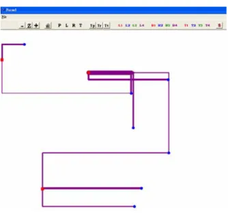
Finally, to avoid the interference between the obstacles and the wire, the proposed method reserves the dead-space for all obstacles. Hence, the benchmark, r1, is taken as the example. The results of wire planning are shown in Figure 4. The results without obstacles are shown in Figure 4(a). Most of the wires go straightly without the less number of bending. The results with the obstacles are shown in Figure 4(b). We observe that most of wires have many number of bending due to the huge number of obstacles. Figure 4(c) show the space between the obstacles and the wires. The proposed method indeed reserves the user-defined space to improve the interference.
V.CONCLUSIONS
In this paper, we propose the graph-based method which determines the proper widths for all wires to avoid the electromigration while minimizing the total wiring area. First, the reservation space technique is used to reduce the interferences between the obstacles and wires. Second, the graph-based method are utilized to determine the topology among the sources and targets according to circuit information after the greedy method is used to generate the feasible routing path with obstacles. Compared to the results without obstacles, our graph-based method leads to additional total area by 9.18% in average.
REFERENCE
[1] T. Adler, H. Brocke, L. Hedrich and E. Barke,
“A Current Driven Routing and Verification Methodology for Analog Applications,” in
Proc. of ACM/IEEE Design Automation Conference, pp. 385-389, 2000.
[2] T. Adler and E. Barke, “Single Step Current
Driven Routing of Multiterminal Signal Nets for Analog Applications,” in Proc. of Design, Automation and Test in Europe, pp. 446-450,
2000.
[3] J.R. Black, “Electromigration Failure Models
in Aluminum Metallization for Semiconductor Devices,” in Proc. of the IEEE, pp. 1587-1594,
1969.
[4] J.R. Black, “Physics of Electromigration,” in
Proc. of IEEE 12th Annual Reliability Physics Symposium, pp.142-149, 1974.
[5] S. Chen, X.L. Hong, S.Q. Dong, Y.C. Ma, Y.C.
Cai, C.K. Cheng, J. Gu, “A Buffer Planning Algorithm with Congestion Optimization,”
Proc of ACM/IEE Asia and South Pacific Design Automation Conference, pp. 615-620,
2004.
[6] C. Chiang, Q.Su, and C. S. Chiang,
“Wirelength Reduction by Using Diagonal Wire,” in Proc. of ACM Great Lakes Symposium on VLSI, pp.104-107, 2003.
[7] A. Davoodi and A. Srivastava, “Effective
Graph Theoretic Techniques for the Generalized Low Power Binding Problem,” in
Proc. of ACM International Symposium on Low Power Electronics and Design,
pp.152-157, 2003.
[8] M. Ekpanyapong and S.K. Lim, “Integrated
Retiming and Simultaneous Vdd/Vth Scaling for Total Power Minimization?” in Proc. of ACM the International Symposium on Physical Design, pp.142-148, 2006.
[9] G. Jerke, J. Lienig, and J. Scheible,
“Reliability-driven layout decompaction for Electromigration failure avoidance in complex mixed-signal IC designs,” in Proc. of ACM/IEEE Design Automation Conference, pp.
181–184, 2004.
[10] T.Y. Ho, C.F. Chang, Y.W. Chang, and S.J.
Chen, “Multilevel Full-Chip Routing for the X-based Architecture,” in Proc. of ACM/IEEE Design Automation Conference, pp. 597-602,
2005.
[11] H.H. Huang Y.C. Chen and T.M. Hsieh, “A
Congestion-Driven Buffer Planner with Space Reservation,” in Proc. of IEEE International Symposium on Circuits and Systems, pp.
5435-5438, 2006.
[12] H.H. Huang, S.P. Chang, Y.C. Lin and T.M.
Hsieh, “Timing-Driven X-Architecture Router among Rectangular Obstacles,” in Proc. of IEEE International Symposium on Circuits and Systems, pp. 1804-1807, 2008.
[13] J. Lienig, “Introduction to Electromigration
-Aware Physical Design,” in Proc. of ACM International Symposium on Physical Design,
pp.39-46, 2006.
[14] J. Lienig and G. Jerke, “Current-Driven Wire
Planning for Electrimigration Avoidance in Analog Circuits,” in Proc of ACM/IEE Asia and South Pacific Design Automation Conference, pp. 783-788, 2003.
[15] J. Lienig, G. Jerke, T. Adler, “Electromigration
Avoidance in Analog Circuits: Two Methodologies for Current-Driven Routing,” in
Proc. of ASPDAC/VLSI Design, pp. 372-37,
2002.
[16] J. Lienig, G. Jerke and T. Adlert,
“AnalogRouter: A New Approach of Current-Driven Routing for Analog Circuits,” in Proc. of Design, Automation and Test in Europe, pp. 819-819, 2001.
[17] Z. Shen, C.N. Chu and Y.M. Li, “Efficient
Rectilinear Steiner Tree Construction with Rectilinear Blockages,” in Proc. of IEEE International Conference on Computer Design,
pp. 38-44, 2005.
[18] J.T. Yan Z.W. Chen and D.H. Hu,
“Electromigration-Aware Rectilinear Steiner Tree Construction for Analog Circuits,” in
Proc. of 18-th VLSI Design and CAD Symposium, CD-ROM, 2008.
[19] Y.H. Cheng and Y.W. Chang, “Integrating
buffer planning with floorplanning for simultaneous multi-objective Optimization,” in
Proc. of ACM/IEEE Asia South Pacific Design Automation Conference, pp. 624-627, 2004.
[20] A. Devgan, “Efficient coupled noise estimation
for on-chip interconnects,” in Proc. of IEEE/ACM International Conference on computer-Aided Design, pp. 147–151, Nov.
Table 1. Benchmark circuits.
circuit No. of obstacle R ob No. of terminal No. of source No. of target
R1 10 8.2 10 3 7
R2 10 21.7 50 16 34
R3 10 39.4 70 23 47
R4 10 29.2 100 33 67
R5 300 10.7 200 66 134
Rob denote the ratio between the obstacle and the chip area.
Table 2. Comparison of the wiring area of greedy graph-based method without and with obstacle.
Table 3. Explore relationship betweenR and additional area. ob ob
R (%) I (WITHOUT) II (WITH) Addition_area
R1 8.2 487160.0 520640.0 6.9
R2 21.7 1407820.0 1669400.0 18.6
R3 39.4 2415290.0 2510870.0 4.0
R4 29.2 2413740.0 2657820.0 10.1
R5 10.7 4098359.0 4356453.0 6.3
I (WITHOUT) II (WITH) Addition_area Area1 Time1 Area2 Time2 100 (Area2-Area1)/Area1×
R1 487160.0 0.0 520640.0 0.015 6.9 R2 1407820.0 0.015 1669400.0 0.046 18.6 R3 2415290.0 0.031 2510870.0 0.046 4.0 R4 2413740.0 0.031 2657820.0 0.078 10.1 R5 4098359.0 0.062 4356453.0 0.203 6.3 AVG - - - - 9.18
(a) The wire planning without obstacles
(b) The wire planning with obstacle
(c) Local view of (a)