高介電常數材料(HfAlO)沉積前後表面處理之研究
71
0
0
全文
(2) 高介電常數材料(HfAlO)沉積前後表面處理之研究. Investigation Investigation of Surface Treatment Treatment Before and After After Highigh-k(HfAlO) Dielectric Deposition. 研 究 生 : 陳彥銘. Student:Yen-Min Chen. 指導教授 :羅正忠. Advisor:Jen-Chung Lou. 國 立 交 通 大 學 電子工程學系. 電子研究所碩士班. 碩 士 論 文 A Thesis Submitted to Department of Electronics Engineering & Institute of Electronics College of Electrical and Computer Engineering National Chiao Tung University in partial Fulfillment of the Requirements for the Degree of Master of Science in Electronics Engineering July 2007 Hsinchu, Taiwan, Republic of China. 中. 華 民. 國. 九 十 六. 年. 七. 月.
(3) 高介電常數材料(HfAlO) 高介電常數材料(HfAlO)沉積前後表面處理之研究 (HfAlO)沉積前後表面處理之研究. 研 究 生: 陳 彥 銘. 指導教授: 指導教授: 羅 正 忠 博士. 國 立 交 通 大 學. 電子工程學系. 電子研究所碩士班. 摘要. 近年來很多研究致力於發展可替代二氧化矽介電層材料,用高介電常數取 代二氧化矽的方法使得半導體的元件能夠持續發展下去,並且克服物理上 縮小的限制,在高介電常數的材料中,二氧化鉿是較有潛力的高介電常數 材料,它有較高的介電係數跟跟載子能障,且與矽反應所需能量較高,如 果我們在沉積二氧化鉿時,參雜一些三氧化二鋁可以提高結晶溫度,增加 熱穩定性,但由於鋁堆積在介電層與矽之間的介面,依然有固定負氧化物 電荷的問題,使得遷移率下降。因此在介電層與矽基板之間的介面層就變. i.
(4) 得很重要,它的品質會影響到元件的特性還有可靠度等。所以在本論文 中,我們比較用二氧化氮和紫外光加臭氧表面處理形成的一層薄膜類似二 氧化矽,看哪種表面處理對元件的特性有較好的影響。 在另一方面,經過表面處理可能會改變介電層的主要鍵結,減少在金屬與 介電層介面或介電層中的缺陷,我們用 NH3 電漿與紫外光加臭氧兩種表面 處理伴隨之後適當快速熱退火溫度來改變介電層中的主要鍵結,看是否對 電性能有正面的影響。從磁滯效應,漏電流,電容,可靠度,等效二氧化 矽厚度等特性來看,紫外光加臭氧的前處理以及 NH3 電漿伴隨 800℃的後 處理能夠達到較好的電性。. ii.
(5) Investigation of Surface Treatment Treatment Before and After HighHigh-k(HfAlO) Dielectric Deposition. Student: Yen-Min Chen. Advisor: Dr. Jen-Chung Lou. Department of Electronics Engineering and Institute of Electronics National Chiao Tung University, Hsinchu, Taiwan. Abstract In recent years, a lot of research effort has been focused on developing alternative gate dielectric materials to replace SiO2. Using high dielectric constant provide the way to make the semiconductor roadmap go on, and overcome the present physical limits of semiconductor scaling down. Among High-k materials, HfO2 can be used due to its relatively high dielectric constant, its relatively high free energy of reaction with Si, and its relatively high band gap, and if we add Al during deposition process to form HfAlO can increase crystallization temperature, and have better thermal stability than HfO2, but HfAlO also introduces negative fixed oxide charges due to Al accumulation at the HfAlO-Si interface, resulting in mobility degradation, therefore the control of SiO2-like interface between high-κ dielectrics and silicon substrate pays more and more important, since the device performances and reliability characteristics are strongly affected by the interface quality. In this thesis we compare Nitridation of the Si surface using N2O and Oxidation of the Si surface using UV ozone prior to the deposition of high-κ gate dielectrics to see iii.
(6) which is good for the electrical properties of devices. In the other hand the interface treatment can change the texture bonding, and reduce defects such as dangling bonds at the interface between metal gate and dielectric as well as incorporation of extra impurities. The changes of interface and incorporation will upset a balance within the primary interface, we use UV ozone and NH3. two treatment accompany with appropriate RTA temperature to change the texture bonding and see which improve the electrical properties effectively. In this thesis we find a suitable surface treatment before and after HfAlO deposition and appropriate annealing temperature to improve electrical characteristics. From the hysteresis , leakage current density, capacitance, reliability, EOT, etc. the UV ozone pre-treatment and NH3 post treatment with 800℃ RTA has excellent electrical characteristics.. iv.
(7) 誌謝 首先感謝我的指導教授羅正忠博士,在老師的課程與平時的指導中,得 到許多知識,以及做研究的方法與觀念態度,也感謝老師提供的實驗室資 源,不時的給我指導,建立深厚的研究基礎, 讓我在這兩年的碩士生涯 中,能順利的完成這篇碩士論文,在這也謝謝我的口試委員龔正教授,張 國明教授,能夠在百忙之中,抽空前來聽學生口試,此外還要感謝世璋學 長無條件的指導,在困難時給我適時的援助,不論在學問上或做人處事上 都受益良多,還要感謝 韶華,一桀學長,忠樂,阿國,振欽,俊宏,人 傑,建彰,在課業上對我的幫忙,以及 裕威,卓基,澤宇,猗靂,怡蓁, 意婷,奕穎,盈鋅,郁晴,維謙,慎千,在生活上的幫忙,能夠替我紓解 平日生活的壓力,沒有你們,也是無法讓我順利畢業的,另外也要對國家 奈米實驗室,交大奈米中心的各個工程師以及阿姨致上深深的謝意,在機 台有問題有妳們的幫忙,才得以讓實驗順利進行。最後,最應該感謝的還 是我的家人父親陳添進先生,母親黃秀英女士,感謝你們多年的栽培,讓 我在學業上能夠劃下一個完美的句點,還有哥哥禹伸的激勵與支持,有家 人們的支持,才能讓我無後顧之憂的完成碩士學位。 ,. v.
(8) Contents Abstract (Chinese) ..……………..……..…………………..…………….……i Abstract (English) ..…………………………….……………….…………….iii Acknowledgment (Chinese) ………………………...………………….……..v Contents …………………………………...………………….……………....vi Table Captions………………………………………………………………..viii Figure Captions ……………………………………………………................ ix. Chapter.1 Introduction 1.1 General Background ……………………………………………...1 1.2 Motivation ……………………………...........................................3 1.3 The choice of Hig-k Materials………….........................................3 1.4 Fermi Level pinning ………………………………………………5 1.5 Organization of This Thesis…………………………………….....7 Chapter.2 Experimental Procedures and Measureme 2.1. Properties of Hafnium Aluminum Oxide …………………...….13. 2.2. Experiment Process of PMOSFET with Treatment Before HfAlO Deposition…………………………………………..….13. 2.3. Experiment Process of Capacitance with Treatment Before and After HfAlO Deposition………………………………………..14. 2.4. Interface Treatments Before HfAlO Deposition………………..15. 2.5. Interface Treatments After HfAlO Deposition. 2.6. Electrical Measurement…………………………………….…...16. 2.7. Reliability Measurement…………………………………….…..16 vi. ……………….15.
(9) Chapter.3 Result and Discussion 3.1. The Electrical Characteristics of Surface Treatment Before HfAlO Deposition ………………………………………...23. 3.2. Electrical Properties with Surface Treatment After HfAlO Deposition ……………………………………..........25. 3.3. Electrical Properties of Post Dielectric Annealing (PDA)………….26. 3.4. The Trapping Phenomenon of Observation under SILC Stress……27. 3.5. Surface Composition Analysis by X-ray Photoelectron Spectrometer...........................................................................................28. 3.6. The Instruction of Leakage Current Conduction Mechanism............29. 3.6.1 Schottky Emission……………………………………………......29 3.6.2 Frenkel-Poole Emission…………………………………………..30. Chapter.4 Conclusions and Recommendations for Future Works 4.1. Conclusion…………………………………………………………....51. 4.2. Suggestions for Future Work………………………………………. ..52. Reference ……………………………………………………...……...53. vii.
(10) Table Captions Chapter 1 Table 1-1 properties comparison of SiO2 and HfO2. viii.
(11) Figure Captions. Chapter 1. Fig 1-1. The bandgap of high-k materials. Fig 1-2. The critical Fermi level of metal gate on dielectric.. Fig 1-3. Schematic illustration of the Fermi level pinning observed in poly-Si and n-like, p-like MSix gates. Chapter 2. Fig 2-1. The leakage current of ALD 30nm of HfO2 and HfAlO. after rapid thermal. annealing of 800℃ and 950℃ Fig 2-2. The diagram of process flow of pMOS transistor. Fig 2-3. The cross section of pMOS transistor.. Fig 2-4. The diagram and structure of process flow of capacitance. Chapter 3. Fig 3-1. UV ozone system schematic diagram. Fig 3-2. Id-Vd characteristics with UV ozone and N2O treatment. VG-Vth= 0 ~ -2 V,. Fig 3-3. The transconductance characteristic of HfAlO samples with UV ozone. a Fig 3-4. and N2O surface treatment Id-Vg characteristics of PMOSFET with UV ozone treatment.. ix.
(12) Fig 3-5. Id-Vg characteristics of PMOSFET with N2O treatment.. Fig 3-6. Charge pumping measurement Icp. Fig 3-7. Mobility characteristic of PMOSFET with N2O and UV ozone. E. treatment. Fig 3-8. The relationship between mobility and Nit of HfAlO with UV ozone and N2O surface treatment. Fig 3-9. The C-V curves of O3 and NH3 treatment with 800℃ RTA after HfAlO deposition. Fig 3-10. The J-V curves of O3 and NH3 treatment with 800℃ RTA after HfAlO deposition. Fig 3-11. The leakage current after a gate injection stress of UV ozone and NH3 treatment. Electron trapping is observed in ozone treat samples. Fig 3-12. The normalize C-V curve of HFAlO with UV ozone, NH3 treatment and without treatment samples. Fig 3-13. The C-V curves of as deposited HfAlO. Fig 3-14. The C-V curves of HfAlO after PDA. Fig 3-15. The J-V curves of HfAlO before PDA and after PDA. Fig 3-16. The leakage current after gate injection stress of as-deposited HfAlO. Fig 3-17. The leakage current after gate injection stress of HfAlO with different PDA temperature. Fig 3-18. The J-E curves of as deposited HfAlO samples under SILC stress. Fig 3-19. The J-E curves of HfAlO samples with O3 surface treatment under SILC stress. Fig 3-20. The J-E curves of HfAlO samples with NH3 surface treatment under SILC stress x.
(13) Fig 3-21. The electron binding energies of Si 2p orbital before and after UV ozone surface treatment. Fig 3-22. The electron binding energies of O (1s) orbital before and after UV ozone surface treatment. Fig 3-23. The electron binding energies of C orbital before and after UV ozone surface treatment. Fig 3-24. The electron binding energies of O (1s) orbital with NH3 treatment with different RTA temperature. Fig 3-25. The electron binding energies of N(1s) orbital with NH3 treatment with different RTA temperature. Fig 3-26. The electron binding energies of HF(4f) orbital with NH3 treatment With different RTA temperature. Fig 3-27. Schematic band diagram of Schottky emission. Fig 3-28. Schematic band diagram of Frenkel-Poole emission. Fig 3-29. The conduction mechanism fitting of HfAlO samples with UV ozone treatment .. Fig 3-30. The conduction mechanism fitting of HfAlO samples with NH3 treatment .. xi.
(14) Chapter 1. Introduction. 1.1 General Background. The novel metal-oxide-semiconductor (MOS) technology has kept developing alone the moore’s law “the device will scale down every eighteen month” By the improvement of semi-conductor technology, in order to lower costs, the devices in the integrated circuit must be increased, therefore the size of devices must be scaled down. In respect of dielectric, for maintaining the fixed power density, when the length of channel. decreased,. the. thickness. of. dielectric. also. must. be. decreased,. especially when the thickness of oxide dielectric is lower than 2nm. The viability of SiO2 will face severe challenge such as increasing gate leakage has become a serious issue because of tunneling effect. Even if thermal oxide have several advantages , for example high quality interface, good thermal stability, being amorphous phase throughout the integration process and can have low leakage current, but the thickness of. SiO2 will reach the predicted limits of scaling, therefore high-k. dielectric are possible replaced for SiO2 because of its high dielectric constant. In recent years, a lot of research effort has been focused on developing alternative gate dielectric materials to replace SiO2. Using high dielectric constant provide the way to make the semiconductor roadmap go on, and overcome the present physical limits of semiconductor scaling down. Therefore the applications of high dielectric constant materials become a trend in semiconductor technology below the 100nm 1.
(15) dimensions. [1]~[4]. 1.2 Motivation. With the improvement of the process technology, when the devices scale down, how to suppress the leakage current effectively is our target. The shrinkage of channel length is the most effective way to promote the driving current of a transistor. Another way to improve the Ids is increasing the Cox (eq-1) by scaling down oxide thickness (eq-2), therefore finding High-k materials, and making them have thicker true thickness but have thinner EOT (Equivalent Oxide Thickness), is one of our researching direction.. Ids = 1/2Coxµn(W/L)(VGS-Vt)(VDS). [eq-1-1]. Where µn is the effective mobility, Cox is the gate capacitance, W is the channel width, L is channel length. Obviously, drive current is inversely proportional to the channel length L. Therefore, the shrinkage of channel length is the most effective way to promote the driving current of a transistor.. [eq-1-2] Generally there are several point we should care about high-k materials (1) low. 2.
(16) leakage current. (2) low interface trap density. (3) low bulk trap. (4) good thermal stability. (5) good reliability. But now the subject matter of high-k materials is the high interface trap density lead to high leakage current and not available to work on devices. Therefore, this thesis is researching different surface treatment after depositing high-k materials to lower interface trap and abate Fermi level pinning effect. We expect that it is useful to increase high-k materials feasibility and will replace SiO2 in the future.. 1.3 The Choice of High-K Materials. There are many factors we should think about when we choose high-k materials. First, the most of high-k materials don’t have wide enough bandgap, therefore it is easy for both electron and hole through the dielectric, and lead to large leakage current. The bandgap of high-k materials are present in. Fig1-1.. Second, materials with slightly high-k value than thermal oxide don’t have low leakage enough to conform to our criteria, and large k value materials have poor thermal stability generally, and will suffer from larger fringing field and degrade short channel characteristics [5], the fringing effect will make extra field lines terminate in the S/D region and share the charge controllability with the gate. This will lower the potential in the channel for electron, and influence the gate control ability. Third, most of high-k would react with the Si, there are two possible reaction, one is [eq1], after the high temperature process, the metal in high-k materials would separate out, and the oxygen would react with the Si to form an interfacial layer between silicon subtract and high-k. 3.
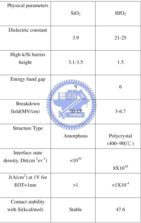
(17) MOx + Sii → M + SiO2. [eq1-3]. The other is the high-k materials react with Si to form silicide [eq4], the formation of the silicide would provide the transport path to carrier, and induce large leakage current. MOx + Sii → MSiy + SiO2. [eq1-4]. The interfacial layers would lower dielectric constant, therefore the dimension size will hard to scale down. Fourth, the interface quality and morphology between high-k and Si substrate should be considered. The quality would affect the carrier mobility in the channel, and make mobility degradation, lower the device performance. Another aspect, the film morphology is also important, during the all process, the device has to go through many high temperature thermal treatment, including annealing, dopant activation annealing, the thermal budget will affect the film morphology, high temperature process would make high-k dielectric change phase, from the amorphous phase to the polycrystalline phase, lead to large grain boundaries which supply leakage path and induce large leakage current. Considering all of above, we should choose the appropriate high-k material with more advantage and less drawback to device. Among High-k materials, HfO2 can be used due to its relatively high dielectric constant(~25), its relatively high free energy of reaction with Si, and its relatively high band gap(5.68ev), the properties comparison of SiO2 and HfO2 is showed in table 1-1. If we add Al during deposition process to form HfAlO can increase crystallization temperature, and the concentration of Al is higher, the crystallization temperature is higher too . If the crystallization. 4.
(18) temperature is low, grain boundaries in crystallized gate dielectric can be the fast paths for oxygen or dopants diffusion into gate dielectric and even into FET channel region in silicon substrate causing uncontrolled interfacial layer growth at the high-K/Si interface, threshold voltage instability and defect generation. Adding Al during deposition process can also prevent the formation of Hf silicide between dielectric and Si substrate. Therefore, HfAlO can have better thermal stability than HfO2, but HfAlO also introduces negative fixed oxide charges due to Al accumulation at the HfAlO-Si interface, resulting in mobility degradation.. 1.4 Fermi Level Pinning. There is a problem when we use high-k dielectric, the phenomenon is called Fermi level pinning (FLP) and it will make the effective work function of gate materials be controlled difficultly. It means that Φm,eff. differs from Φm,vac, therefore the. flatband voltage is almost independent upon metal gates, FLP is a consequence of interfacial reaction or interfacial charge exchange between gate electrode and gate dielectric, the reasons of Fermi-level pinning is intrinsic charge exchange. The MIGS (metal induced gap states) and VIGS (virtue gap states) theory are used to explain the intrinsic charge exchange, The origin of the VIGS is from the dangling bonds of uncoordinated surface atoms. These dangling bonds produce surface states which continuously disperse in the energy gap of dielectrics. The surface states are confined at the surface to exponentially decay into vacuum and into solid . MIGS assumes that the exponentially decaying bulk states are the main component of the 5.
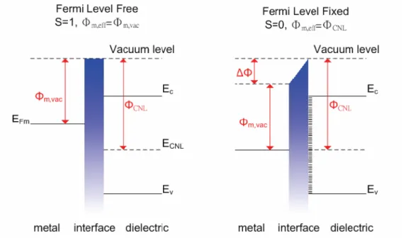
(19) surface states of the dielectric and that the states of the metal in contact with the dielectric couple to its surface states exchanging in order to maintain local charge neutrality. Free electrons in the metal penetrate into the dielectric at the interface and cause the interface charges. The amount of transferred charges is dependent upon the charge neutrality level (ECNL) and metal Fermi level (EFm). ECNL is a branch point of surface energy level, which is usually near the mid-gap of dielectric energy band. No charge will be transferred across the interface when the EFm is coincided with ECNL. With the surface level above or below ECNL, the net charge of the surface is negative and positive on the dielectric side, respectively. In the case where EFm is above ECNL, the dipole layer created at the interface will be negative on the dielectric side. This dipoles will tend to drive the EFm close to ECNL, and hence the effective work function (Φm,eff) will differ from the work function in vacuum (Φm,vac). The effective work function takes account the effects of interfacial dipoles and is determined by. Φm,eff =ΦCNL + S(Φ S(Φm,vac-ΦCNL). [eq-1-4]. Where S is the dielectric pinning strength, it is the function of the surface density of states. N, the surface states penetration depth δ, and the permittivity of the. dielectric. (eq 1-5). And it also can be estimated from the empirical (eq 1-6) S=( S=(1+e2Nδ/εs). [eq-1-5]. S= [1 + 0.1 (ε (ε∞-1)2 ] -1. [eq-1-6]. 6.
(20) whereε∞ [6] is the electronic component of the dielectric constant.. Figure 1-2 shows two critical conditions, Fermi Level Free S=1, and Fermi Level Fixed S=0. A high-k dielectric will lower the slope parameter S and highly pin the Em,eff in the ECNL since the electronic component of the dielectric constant is high. This indicates that high-k materials will suffer from serious Fermi-level pinning effect, and induce effective work function close to ΦCNL. To obtain suitable effective work function, metal gates on high-k materials for pMOSFETs (nMOSFETs) should have higher (lower) work function to compensate the effects of Fermi-level pinning. Another theory is that Fermi level pinning in high work function materials is governed by the O vacancy generation and subsequent formation of interface dipole near gate electrodes due to the electron transfer, and it in low work function is governed by O interstitial formation, therefore the work function pinning free region appears due the difference in the mechanism of Fermi level pinning of high and low work function materials. And the type of metal silicide is also affect the pinning position, n-like metal silicides. are usually located. between the pinning position of n+ and p+ poly-Si gate, and those of p-like metal silicides are located near the pinning position of p+-poly-Si gates , the pinning position is shown in Figure1-3. 1.5 Organization of This Thesis .In this thesis have four chapters in this dissertation. In chapter 1 , we make an introduction to describe the background of the Semiconductor technology and. 7.
(21) discuss the possible issues that we may meet during the dimensions scaling down. In addition , we would talk about the hopeful solutions to overcome the physical limits. The possible solution is the alternative high dielectric constant materials. They would replace the traditional SiO2 material in the gate materials.In chapter 2 , we will introduce the properties of the high dielectric constant material hafnium oxide ( HfAlO ), and describe the experimental procedures, electrical measurements, material analysis. In chapter 3 , we will investigate the electrical properties of HfAlO thin film including two surface treatment UV ozone treatment and N2O treatment. before HfAlO deposition and two interface treatment UV ozone treatment and NH3 treatment accompany with RTA treatment after HfAlO deposition We will discuss the experimental results.At the end of this thesis, conclusions are given in chapter 4.. 8.
(22) 1.6. 3.3. Fig 1-1 The bandgap of high-k materials. 9.
(23) Physical parameters SiO2. HfO2. 3.9. 21-25. 3.1-3.5. 1.5. 9. 6. 10-15. 3-6.7. Amorphous. Polycrystal (400~900℃). Dielectric constant. High-k/Si barrier height Energy band gap. Breakdown field(MV/cm) Structure Type. Interface state density, Dit(cm-2ev-1). <1010 8X10¹⁰. J(A/cm2) at 1V for EOT=1nm. >1. <1X10⁻⁴. Stable. 47.6. Contact stability with Si(kcal/mol). Table 1-1 properties comparison of. 10. SiO2 and HfO2.
(24) Figure 1-2. The critical Fermi level of metal gate on dielectric. the effective work function of metal on dielectric is the same as in vacuum while the interface is perfect. The work function is fixed to the dielectric-charge-neutral level while the interface-state density is high. the interface states are caused by both intrinsic states (MIGS, ViGS) and extrinsic states (defect levels).. 11.
(25) Fig 1-3. Schematic illustration of the Fermi level pinning observed in poly-Si and n-like, p-like MSix gates 12.
(26) Chapter 2. Experimental Procedures and measurements 2-1. Properties of Hafnium Aluminum Oxide. HfAlO film was deposited by electron-beam evaporation method. The background pressure of the main chamber was 10−6–10−7 Pa, and the substrate temperature was kept at 300 °C. High purity sintered HfO2 and Al2O3 pellets were coevaporated at the rate of 0.2–0.5 Å/ s, We use Hafnium aluminum oxide (HfAlO) to replace Hafnium oxide (HfO2), because of the some poor characteristics of HfO2.[7] When the HfO2 is thin, it exhibit poor thermal stability and tend to crystallize at low temperature of 400-500℃, this will cause significant increases in leakage current, therefore it can increase crystallization temperature by the incorporation of Al2O3 forming the HfAlO alloy [8]-[12].. The comparison of leakage current in different annealing temperature of this two materials is showed in Fig 2-1. we can observed the leakage current of HfO2 at higher temperature is larger than HfAlO at same RTA temperature.. 2-2. Experiment Process of PMOSFET with Treatment Before HfAlO Deposition MOS transistors was fabricated on 4-inch p-type Si with ( 1 0 0 ) orientation.. After removing the native oxide, RCA clean was performed with HF-dip last, followed by UV ozone and N2O treatment. After surface treatments sample with a high temperature 900oC 60 seconds was used for density interface oxide. After. 13.
(27) surface treatment HfAlO was deposited at room temperature and 7.6E-3 torr by ion sputter system. Followed by a high temperature 900oC post deposition annealing (PDA) in the nitrogen ambient for 30 seconds in order to improve the film quality. A 200nm undoped polycrystalline silicon (poly-Si) layer was directly deposited by low pressure chemical vapor deposition (LPCVD) on top of HfAlO films After the gate electrode was patterned by lithography and etching processing. Then implant As 20 KeV dose 5E15 #/cm2 after that activation was done at 950 oC by rapid thermal annealing (RTA) for 30seconds in the nitrogen ambient. After a 500nm SiO2 passivation was done by PECVD. Define the contact hole by the lithography and etching passivation SiO2 and high k layer in order to silicon contact whit metal. Al was deposited by thermal evaporation system. Metal pad is defined by lithography and etching. Backside contact was formed by thermal evaporation. Fig 2-2 , Fig2-3 show the cross section and the process flow of pMOS transistor.. 2-3. Experiment Process of Capacitance with Treatment Before and After HfAlO Deposition. Wafers were cleaned by standard RCA processes with HF-last for the removal of the particles and native oxides. and UV ozone was used to grow an ultra-thin ozone oxide about 9~11Å, after UV ozone surface treatments, a high temperature 900oC 60 seconds was used for densify ozone oxide. HfAlO was then deposited at room temperature and 7.6E-3 torr by ion sputter system, followed by UV-ozone or plasma NH3 treatment and then a different high temperature (as deposition, 800oC, 900oC,1000oC) post deposition annealing (PDA) in the nitrogen ambient for 60 seconds were investigated, before Aluminum metal gate deposition which was created by a thermal evaporation system. After gate electrodes patterned and. 14.
(28) backside contact was formed by thermal evaporation. The process flow and structure are shown in Fig 2-3, the area of capacitors is 4.5216×10⁻⁴ cm2. 2-4. Interface Treatments Before HfAlO Deposition. The control of SiO2-like interface between high-κ dielectrics and silicon substrate pays more and more important, since the device performances and reliability characteristics are strongly affected by the interface quality. Nitridation of the Si surface using N2O prior to the deposition of high-κ gate dielectrics has been shown to be effective in achieving the low EOT (equivalent oxide thickness) and preventing boron penetration [13], [14]. However this technique results in higher interface charges [15], which leads to higher hysteresis and reduced channel mobility. Ozone-formed oxide (ozone oxide) has superior characteristics. Even when the formation temperature is less then 400°C, ozone oxide has a high film density comparable to that of the device-grade oxide film formed at higher temperature, a low interface trap density, and a much thinner structural transition layer near the SiO2/Si interface [16]. The ozone surface treatment was employed to improve the interface quality between HfAlO and silicon substrate.. 2-5. Interface Treatments After HfAlO Deposition. The interface treatment can be performed with the surface treatment before metal deposition and it can be plasma treatment or reactive gas annealing. The interface treatment can change the texture bonding, and reduce defects such as dangling bonds at the interface between metal gate and dielectric as well as incorporation of extra impurities. The changes of interface and incorporation will upset a balance within the primary interface. According the past research the direct contact of high-k materials 15.
(29) and Si-substrate will have many issues. We need high quality interface of dielectric/Si. or metal/dielectric with low density of interface states (Dit~2x10¹⁰. states/cm2) arising from unsaturated surface bonds and other electrically active imperfections. Interface states will lead to low on-current because of carrier mobility is limited by scattering at the interface with the vertical electric fields present in the channel. Therefore in this thesis we try two surface treatment including ozone plasma and NH3 plasma after HfAlO deposition to make the higher quality interface between metal gate and high-k dielectric, or change the texture bonding of HfAlO.. 2-6. Electrical Measurement. The Capacitance-Voltage (C-V) and Current-Voltage (I-V) characteristics were measured by Hp-4284 and Hp-4156. The dielectric constant (k-value) is then calculated from the measured capacitance at accumulation mode. The equivalent oxide thickness (EOT) was extracted by fitting the measured high-frequency (100 kHz) capacitance-voltage (C-V) data under accumulation condition. UCLA CVC simulation program was utilized to obtain the accurate flat band voltage (VFB). The C-V hysteresis phenomenon was measured by sweeping the gate voltage from accumulation to inversion then back. The tunneling leakage current density-electric field (J-E) and the reliability characteristics of MOS capacitors were measured by semiconductor parameter analyzer HP 4156C.. 2-7. Reliability Measurement. We observe the reliability from stress-induced leakage current (SILC),, measurements. SILC were measured at room temperature, gate bias=--4 for RTA after. 16.
(30) surface treatment and -3V for RTA before surface treatment, the J-E curves were measured at 10 sec 20sec 50sec 100sec 200sec 1000sec respectively during stress.. 17.
(31) 10-2. PDA 800 for HfAlO PDA 950 for HfAlO PDA 800 for HfO2. 10-3. PDA 950 for HfO2. 2. Gate current (A/cm ). 10-1. 10-4 10-5 10-6 10-7 10-8 10-9 -3.5. -3.0. -2.5. -2.0. -1.5. -1.0. -0.5. 0.0. Gate voltage. Fig 2-1. The leakage current of ALD 30nm of HfO2 and HfAlO after rapid thermal annealing of 8000℃ and 9500℃. 18.
(32) Define by Lithography and pattered. Define Active region. RCA Clean with HF-last. One is Ozone surface treatment and the other is N2O treatment.. Surface Treatment. High_k Deposition. RTA 800oC 60seconds was used.. Post Deposition Annealing. A 200nm poly silicon was deposited by LPCVD.. Poly Gate Deposition. Define by Lithography and pattered. Define Gate & Patterning. Implant As 20KeV dose:5e15#/cm2. Ion implant. RTA 950oC 30seconds was used and S/D was formed.. Activation. Passivation Oxede Deposition. 19. A 500nm silicon dioxide was deposited by PECVD..
(33) Define by Lithography then etching passivation oxide and high_k.. Define Contact hole & Patterning. 500nm aluminum was deposited by thermal evaporation system.. Aluminum Deposition. Define by Lithography and pattered. Define metal and etching meatal. 500nm aluminum was deposited by thermal evaporation system.. Backside contact. Fig 2-2. The diagram of process flow of pMOS transistor. 20.
(34) Al Pad Passivation Oxide FOX. FOX. Poly Gate S. D. Surface treatment High k Gate dielectric Si Substructure. Al Backside Contact. Figure 2-3 The cross section of pMOS transistor.. 21.
(35) Si-Substract Uv-ozone treatment and densify by RTA 900℃ ℃ 60s flowed HfAlO deposition (100Å). HfAlO. uv-ozone oxide. Si-Substrate Si-Substract Surface treatment by UV-ozone or NH3. HfAlO. Si-Substrate Si-Substract RTA 800℃ ℃ 60s. Al. HfAlO HfAlO. Si-Substract Al. Top electrode Al 5000Å deposition by E-gun Backside contact Al 5000Å deposition by coater Fig 2-4. The diagram and structure of process flow of capacitance. 22.
(36) Chapter 3. Result and Discussion. 3-1 The Electrical Characteristics of Surface Treatment Before HfAlO Deposition Nitridation of the Si surface using N2O prior to the deposition of high-κ gate dielectrics has been shown to be effective in achieving the low EOT and preventing boron penetration [17], [18]. However this technique results in higher interface charges [19], which leads to higher hysteresis and reduced channel mobility. So we use UV ozone to oxidation, ozone and atomic oxygen, produced by exposure of atmospheric oxygen to ultraviolet radiation, Figure 3-1 showed the schematic diagram of UV ozone system. The ozone generator (AnserosPAP-2000) decomposed the oxygen molecular to generate ozone gas by high electrical field. The ozone gas was mixed with UV lamp in chamber. By changing the oxygen flow and ozone generation power, the ozone concentration in the chamber could be adjusted. Ozone-formed oxide (ozone oxide) has superior characteristics. Even when the formation temperature is less then 400°C, ozone oxide has a high film density comparable to that of the device-grade oxide film formed at higher temperature [20], a low interface trap density [21], and a much thinner structural transition layer near the SiO2/Si interface [22]. The ozone surface treatment was employed to improve the interface quality between HfAlO and silicon substrate. Figure 3-2 shows the drain 23.
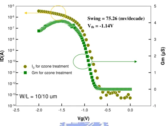
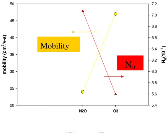
(37) current (Id) versus the drain voltage (Vd) characteristic for UV ozone surface treatment and N2O surface treatment. The drain current is larger for the UV ozone surface treatment. Fig 3-3 shows the transconductance characteristics, we observe that transconductance peak value of UV ozone treatment is higher than samples with N2O rsurface treatment. Figure 3-4 and Figure 3-5 shows the drain current (Id ) versus the gate voltage (Vg) of. pMOSFETs with and UV ozone treatment and N2O. treatment. We can see that the substhreshold swing (S.S.) of. UV-ozone treatment. is 75.26 mV/decade which is better than the 91.2mV/decade of N2O treatment. In this section, we also research the relationship between charge pumping and mobility through devices in different surface treatment.. Unlike SiO2 films, high-k. films are more susceptible to charge trapping. Charge trapping is arguable one of the most important issue in CMOS devices with high-k gate dielectrics, because of the large amount of bulk traps present in the high k films [23]-[26]., and they may cause mobility degradation [27]-[30] and Vth instability [31]-[40], it used to use charge pumping to measure interface state density in MOSFET devices by utilizing the exclusion of gate leakage to calculate interface state density in high-k dielectric. We consider an p-channel device of gate length L and width W Evaluate mobility by Spilt-CV technique. Figure 3-7 shows electron mobility with UV ozone and N2O surface treatment measured by split-CV method. From the mobility we can find that UV ozone treatment have higher mobility, it may be due to the UV ozone treatment have lower Icp and Nit shows in Fig 3-6 and from Fig 3-8 we can make a conclusion that high interface states lead to low mobility. . We compare to this two samples on electrical characteristic above. We found that UV ozone treatment effectively improve the electrical characteristics, such interface state density, electric mobility, transconductance and etc.. 24.
(38) 3-2 Electrical Properties with Surface Treatment After HfAlO uuuDeposition We use uv-ozone, NH3 two surface treatment after HfAlO deposition. Figure 3-9 shows the comparison of the C-V curves of the samples with UV ozone or NH3 surface treatment , both ozone and NH3 surface treatment will reduce leakage current , but samples with NH3 post treatment accompany annealing reduce more, in Figure 3-10, the comparison of J-V curve of the samples with UV ozone or NH3 surface treatment , the NH3 treatment samples have lower leakage with thinner EOT , to sum up, samples with NH3 treatment have large capacitance and lower leakage current with thinner EOT. It may be due to RTA after NH3 treatment will make N diffuss into the HfAlO and form HfAlOxN and make partial change of the local coordination from O-Hf-O to O-Hf-N. The increase of O-Hf-N component drastically degraded the gate leakage current in HfAlOx(N) film [41]. Fig 3-11 shows the leakage current after gate injection stress with UV ozone, and NH3 treatment , trapping is observed obviously in UV ozone treatment samples. It may be due to there are large fixed charge and interface states at interface, therefore the trapping is observed after gate injection stress. We also look from the other side ,Figure 3-12 shows the normalize C-V curve, The C-V curve of NH3 surface treatment was similar to that of HfAlO, indicating that no additional fixed charge was generatede.. 25.
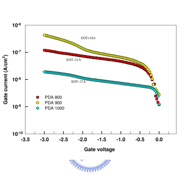
(39) 3-3. Electrical Properties of Post Dielectric Annealing (PDA). Fig 3-13 shows the capacitance-voltage curves of the as deposited HfAlO sample after NH3 surface treatment. There is clear that the scan from inversion to accumulation has a little shift with the scan from accumulation to inversion scan, this suggest that the interface quality is poor, and the film may be a mixing phase of amorphous and polycrystalline at 400℃ deposition, it may be have many imperfect bonds and defects due to incomplete crystal structure and it will lead to plentiful interface states exist at interface to be the trap centers and reduce the mobility. Therefore we try post dielectric annealing at different temperature to see weather can be improving the quality of interface and lower the interface states. Fig 3-14 shows the C-V curve of HfAlO samples with 800℃ 900℃ 1000℃ PDA, and it is clear that the shift is reduced compare to the samples without PDA. PDA treatment at higher temperature after NH3 treatment improved the flat-band voltage shift. Besides improve the quality of interface, we also observe the PDA 1000℃ capacitance at accumulation is smaller than PDA 800℃, It suggests that the increasing thickness of interfacial layer would raise the CET and reduce the dielectric constant. Fig 3-15 shows the current density- voltage curve of the HfAlO samples with different PDA temperature 800℃ 900℃ 1000℃. Higher annealing temperature as 800℃ 900℃ lead to higher leakage due to high annealing temperature trigger small grains to merge into a large grain, and it will provide short leakage path with the boundaries around the large grains which lead the carries tunnel from top electrode to bottom electrode, Therefore the leakage current would increase. But for 1000℃ the leakage current is fall away, it may be due to the thicker interfacial layer resist leakage current, 26.
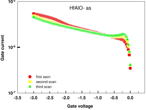
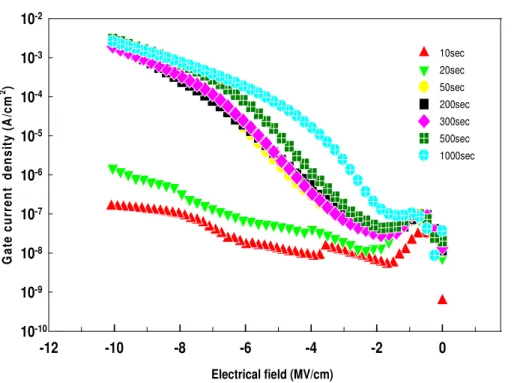
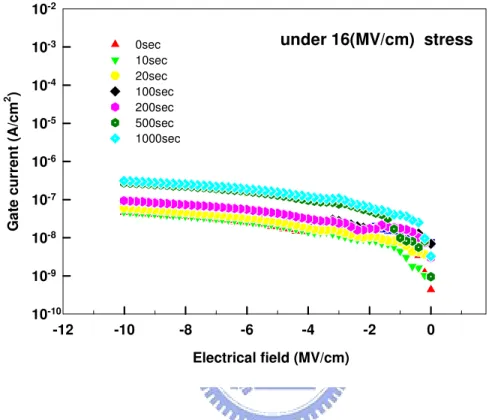
(40) therefore the curve will drop. Fig 3-16. shows the current- electrical field curves of. the HfAlO with no PDA, We can observe that samples with no post dielectric annealing have more trap and the interface quality is not good lead to the obvious different with first scan and second scan, and electron trapping is saturated after the second injection. Fig 3-17 , shows the current-electrical field curves of the HfAlO with different PDA temperature, 800℃ 900℃ 1000℃, it is clear that the result of first scan and second scan are almost the same, therefore trapping is eliminated after annealing, it may due to high temperature can reduce defects in high-k, so PDA can suppress the trapping.. 3-4. The Trapping Phenomenon of Observation Under SILC Stress. For Figure 3-18 ~ Figure 3-20 shows the J-E curves of as deposited samples and with, O3 and NH3 surface treatment under SILC stress. The result we compare samples with treatment and without treatment, that the trapping phenomenon after surface treatment is not severe as the as deposited HfAlO, therefore surface treatment can reduce trap generation under stress .In the other aspect we observed NH3 treatment is superior to UV ozone treatment in suppressing both electron, hole trappings, and interface trap creation under high-field stress. Interface hardness against hot-carrier bombardment and neutral electron trap generation are also improved.. 27.
(41) 3-5. Surface Composition Analysis by X-ray Photoelectron Spectrometer. We use X-ray photoelectron spectrometer (XPS) to analysis composition of surface films, prior to and after periods of UV/ozone treatment, Fig 3-21 shows the Si(2p) binding energies before and after exposure to UV ozone, and after surface exposure to UV ozone, the XPS Si(2p) binding energy shifted toward that of SiO2 (103.6ev) [42], consistent with the formation of silicon that is coordinated to four oxygen atoms. The sampling depth of XPS, however, is only of the order of 7 Å and thus indicates near complete conversion to form a SiO2 surface layer that is at least 7 Å thick, and Figure3-22, Figure 3-23 show the electron binding energies of. O(1s). and C xps spectra, The main O 1s binding energy is the Si-O type with a binding energy of 534.1 eV we can see the reduction in the amount of carbon and an increase in the amount of oxygen within the converted surface film, the reason for reduction of carbon is may be due to UV/ozone treatment removes up to 89% of the carbon from the resultant surface film [43], leading to an overall stoichiometry close to that of SiO2. Fig 3-26 shows the Hf (4f) binding energy with NH3 treatment accompany with RTA and w/o NH3 treatment, there is shift after NH3 treatment. This result suggests a partial change of the average local coordination structure from O-Hf-O to O-Hf-N after high temperature annealing with NH3 treatment because the elecronegativity of nitrogen is relatively low compared to that of oxygen. The results of the N 1s and O 1s XPS spectra also support this interpretation, shown in Fig 3-24, Fig 3-25. The main O 1s binding energy is the Hf-O type with a binding energy of. 28.
(42) 523.3 ev , therefore the film may turn to the HfAlOx(N) after NH3 treatment and RTA .. 3-6 The Instruction of Leakage Current Conduction Mechanism. For the micro electrical devices, the goal for using insulating thin film is hope this film can insulate completely and without any leakage current, including TiO2 HfO2 SiO2, etc has larger band gap and maintain the structure of amorphous or polycrystalline to reduce leakage current, but on reality there are many physical mechanism can make carriers move in the insulting dielectric and form the leakage current, especially in the very thin film or electrical field is large. There are two classes of leakage current mechanisms in the insulating thin film, one is electrode-limited conduction mechanism, it is determined by the character of emission electrode, for example Schottky emission [44] [45] field emission, it is also called tunneling, and thermionic field emission. Among them, tunneling is divided into direct tunneling and Fowler-Nordheim tunneling (F-N tunneling). The other is Transport-limited conduction mechanism, it is determined by the character of material, for example Ohmic conduction,. Frenkel-Poole emission [46][47],. Hopping conduction and ionic conduction. In this thesis we discussion and analysis the Schottky emission and F-P emission.. 3-6.1 Schottky Emission Under the function with electric field, the electron of metal cross the potential energy barrier from metal electrode to the conduction band of insulator, it is called Scottky emission. Consider a electron at x place from metal surface, use the law of virtual image, it will produce equal positive charge at –x place from metal surface, 29.
(43) the gravitation between electron and positive charge is called image force, the image force would lower energy barrier, it is Schottky effect Fig 3-27 Shows the diagram of Schottky emission, therefore electrons across the potential energy barrier easier via field-assisted and increase leakage current. The leakage current equation is showed in (eq.3-1). [eq. 3-1]. Where β= (e3 /4Πε0ε)1/2 ,A* is effective Richardson constant, ε0 is the permittivity of free space,εis the high frequency relative dielectric constant, KB is the Boltzmann constant(1.38 × 10⁻²³ J/K), ψs is the contact potential barrier. We can find the slope of the leakage current equation. (eq 3-2), so we can draw the log(J/T2) versus E1/2 curve to see whether can receive a straight line to judge whether is the Schottky emission mechanism.. ln. J βs φ = E + lnA* - s 2 T K BT K BT [eq 3-2]. 3-6.2 Frenkel-Poole Emission The theorem of Frenkel-Poole effect is similar to Schottky-emission, the different is that electron is excited from trap center to the conduction band of dielectric by way of thermal excitation via field-assisted, Fig 3-28 shows the diagram of. 30.
(44) Frenkel-Poole emission Usually the dielectric with bigger energy band gap have larger probability to happen Frenkel-Poole emission.. In Fig 3-29, Fig 3-20 the conduction mechanism of the UV ozone-treated and NH3-treated HfAlO was extracted from fine Frenkel-Poole fitting. The current from the Frenkel-Poole. J = B × Eeff × exp( ⇒ ln( J / Eeff ) =. or. ln( J / E eff ) = E act × (. − q (φ B − qEeff / πε HfAlOε 0 ) kT. q q / πε HfAlOε 0 kT. ); B = qµN T. qφ Eeff − B + ln( B ) kT . q ) + ln(aB) ; E act = − (φ B − aqE eff / πε HfO 2 ε 0 ) kT. emission is of the form. where B is a constant related to the trapping density and carrier mobility in the HfAlO film, φB is the barrier height, Eeff is the effective electric field in the SiO2 film, ε 0 is the free space permittivity, εHfAlO is the dielectric constant of HfAlO, k is the Boltzmann constant (1.38 × 10⁻²³ J/K), Eact is a field-dependent effective activation , and T is the temperature (K)., From an Arrhenius plot of Eact [i.e., ln(J/Eeff) vs. (q/kT)], we can obtain Eact and B. The barrier height φB and dielectric constant εHfAlO of HfAlO can then be calculated from the intercept of the y axis and the slope of the fitting curves in the plot of Eact vs.. Eeff , according. to E act = q aqπε k ε 0 ( Eeff ) − qφ B . As indicated in Fig.3-29, Fig 3-30 we obtained excellent linearity for each current characteristic. This tendency indicates that the Frenkel-Poole conduction mechanism is dominant in the Ozone-treated and 31.
(45) NH3-treated samples. It may be due to there are large tunneling effect in the interface. We calculated the value the value of φB for electrons was 0.33 eV. and 0.46 eV. O3. O3 O2. O3 Generator. PUMP UV Lamp. N2. O3 Destructor. Figure 3-1. Wafer PUMP. Hot plate. UV ozone system schematic diagram. 32.
(46) 20. 0V. 0. -0.5V. -20. -1V. -60 -80. -1.5V. -100 -120 -140. N2O O3. Vg-Vt=-2V. -160 -180 -5. -4. -3. -2. -1. 0. Vd(V). Fig 3-2. Id-Vd characteristics with UV ozone and N2O treatment. VG-Vth= 0 ~ -2 V,. 5. 4. 3. 2 Gm for N2O treatment Gm for ozone treatment. 1. 0. W/L = 10/10 um -1 -2.5. -2.0. -1.5. -1.0. -0.5. 0.0. Vg(V). Fig 3-3. The transconductance characteristic of HfAlO samples with UV ozone 33. Gm (µ µS). ID (µ µA). -40.
(47) and N2O surface treatment. 10-5. 5. Swing = 75.26 (mv/decade) Vth = -1.14V. 10-6 10-7. 4. ID(A). Fig10 3-3 -8. 3. 10-9 2 10-10 ID for ozone treatment 10-11. Gm (µ µ S). a. 1. Gm for ozone treatment. 10-12 0 10-13. W/L = 10/10 um. 10-14 -2.5. -1 -2.0. -1.5. -1.0. -0.5. 0.0. Vg(V). 3-4. 10-5. 3.5. 10-6. 3.0. 10-7. 2.5. 10-8. ID (A). Id-Vg characteristics of PMOSFET with UV ozone treatment.. Swing = 91.2 (mv/decade) Vth = -0.747. 2.0. 10-9. 1.5 ID for N2O treatment. 10-10. 1.0. Gm for N2O treatment 10-11 10-12. 0.5 0.0. W/L = 10/10 um. 10-13 -2.5. -0.5 -2.0. -1.5. -1.0. -0.5. 0.0. Vg(V). Fig 3-5. Id-Vg characteristics of PMOSFET with N2O treatment. 34. Gm (µ µS). Fig.
(48) 120. Vth=-0.747. O3 Nit=-5.594X10¹¹. 100. N2O Nit=-7.07X10¹¹. Icp(nA). 80 60 40 20 0. -1.8. -1.6. -1.4. -1.2. -1.0. -0.8. -0.6. -0.4. -0.2. Gate voltage. Fig 3-6. Charge pumping measurement Icp. 200 effective for N2O treatment. 180. mobility (cm2/v-s). universal for N2O treatment 160. effective for O3 treatment. 140. universal for O3 treatment. 120 100 80 60 40 20 0 0.0. 0.2. 0.4. 0.6. 0.8. 1.0. 1.2. effective field (MV/cm). Fig 3-7 E. Mobility characteristic of PMOSFET with N2O and UV ozone treatment 35.
(49) 50. 7.2 7.0. 45. 40. 6.6. Mobility. 6.4. 35. Nit. 30. 6.2. Nit(1011). mobility (cm2/v-s). 6.8. 6.0 5.8. 25 5.6 20. 5.4 N2O. Fig 3-8. O3. The relationship between mobility and Nit of HfAlO with UV ozone and N2O surface treatment. 36.
(50) 800. 600. C (P F ). 400. 200 NH3 O3. 0. as. -3. -2. -1. 0. 1. 2. 3. Gate voltage. Fig 3-9. The C-V curves of O3 and NH3 treatment with 8000℃ RTA after HfAlO deposition. 10-6. Gate current (A/cm2). EOT= 21A 10-7. 10-8. EOT= 23A EOT= 20A. NH3. 10-9. O3 as. 10-10 -2.5. -2.0. -1.5. -1.0. -0.5. 0.0. Gate voltage. Fig 3-10. The J-V curves of O3 and NH3 treatment with 8000℃ RTA after HfAlO deposition. 37.
(51) 10-4 O3 treatment first scan O3 treatment second scan. 10-5. O3 treatment third scan NH3 first scan. Gate current. 10-6. NH3 second scan. 10-7 10-8 10-9 10-10 10-11 -2.5. -2.0. -1.5. -1.0. -0.5. 0.0. Gate voltage. Fig 3-11. The leakage current after a gate injection stress of UV ozone and NH3 treatment. Electron trapping is observed in ozone treat samples. 38.
(52) 1.2. as deposited HfAlO NH3 treatment first scan. normalize capancitance. 1.0. NH3 treatment second scan. 0.8 0.6 0.4 0.2 0.0 1. -2.5. -2.0. -1.5. -1.0. -0.5. 0.0. 0.5. Gate voltage (v). Fig 3-12. The normalize C-V curve of HFAlO with NH3 treatment and without treatment samples. 39. 1.0. 1.5.
(53) 700 600 500. C(PF). 400 300 200 100 C-R C-F. 0. -5. -4. -3. -2. -1. 0. 1. 2. 3. Gate voltage. Fig 3-13. The C-V curves of as deposited HfAlO. 1000 PDA 800 C-F PDA 800 C-R PDA 900 C-F PDA 900 C-R PDA 1000 C-F PDA1000 C-R. 800. C(PF). 600. 400. 200. 0. -3. -2. -1. 0. 1. Gate voltage. Fig 3-14. The C-V curves of HfAlO after PDA. 40. 2. 3.
(54) 10-6. Gate current (A/cm2). EOT=18A. 10-7 EOT~21A. 10-8. EOT~27A. PDA 800 PDA 900 PDA 1000. 10-9. 10-10 -3.5. -3.0. -2.5. -2.0. -1.5. -1.0. -0.5. 0.0. Gate voltage. Fig 3-15. The J-V curves of HfAlO before PDA and after PDA. 41.
(55) 10-5. Gate current. HfAlO- as. 10-6. first sacn second scan third scan. 10-7 -3.5. -3.0. -2.5. -2.0. -1.5. -1.0. -0.5. 0.0. Gate voltage. Fig 3-16. The leakage current after gate injection stress of as-deposited HfAlO. 10-5. HfAlO with different PDA temperature. Gate current. 10-6. 10-7. 10-8 first sacn 800 second scan 800 first scan 900 second scan 900 first scan 1000 second scan 1000. 10-9. 10-10 -3.5. -3.0. -2.5. -2.0. -1.5. -1.0. -0.5. 0.0. Gate voltage. Fig 3-17. The leakage current after gate injection stress of HfAlO with different PDA temperature. 42.
(56) 10-2 10sec. G ate current density (A/cm 2 ). 10-3. 20sec 50sec. 10-4. 200sec 300sec. 10-5. 500sec 1000sec. 10-6 10-7 10-8 10-9 10-10 -12. -10. -8. -6. -4. -2. 0. Electrical field (MV/cm). Fig 3-18. The J-E curves of as deposited HfAlO samples under SILC stress. 10-2. under 16 (MV/cm) stress. 2. Gate current density (A/cm ). 10-3 10-4 10-5 10-6 10-7 10-8 10-9 10-10 -12. 0 sec 10sec 20sec 100sec 200sec 500sec 1000sec. -10. -8. -6. -4. -2. 0. Electrical field (MV/cm). Fig 3-19. The J-E curves of HfAlO samples with O3 surface treatment under SILC stress. 43.
(57) 10-2. 10-4. 2. Gate current (A/cm ). under 16(MV/cm) stress. 0sec 10sec 20sec 100sec 200sec 500sec 1000sec. 10-3. 10-5 10-6 10-7 10-8 10-9 10-10 -12. -10. -8. -6. -4. -2. 0. Electrical field (MV/cm). Fig 3-20. The J-E curves of HfAlO samples with NH3 surface treatment under SILC stress. 44.
(58) without ozone treatment with ozone treatment. Si (2p) o. Si. intensity. R. 101.5ev. 103.6ev o. R o. o. Si. o. o. 90. 95. 100. 105. 110. 115. 120. Binding energy. Fig 3-21. The electron binding energies of Si 2p orbital before and after UV ozone surface treatment. uv ozone treatment as deposited. O(1s). intensity. Si-O 534.1 ~ 534.2 ev. 520. 525. 530. 535. 540. 545. Binding energy (ev). Fig 3-22. The electron binding energies of O (1s) orbital before and after UV ozone surface treatment. 45.
(59) uv-ozone treatment as deposited. intensity. C. 275. 280. 285. 290. 295. 300. Binding energy. Fig 3-23. The electron binding energies of C orbital before and after UV ozone surface treatment. 46.
(60) O (1 s ). Hf-O 532.1~532.3 ev. intensity. as d e p o s it e d w it h N H 3 t r e a t m e n t. 520. 525. 530. 535. 540. 545. B in d in g e n e r g y (e v ). Fig 3-24. The electron binding energies of O (1s) orbital with NH3 treatment with different RTA temperature. N (1s). as deposited with NH3 treatment. 380. 385. 390. 395. 400. 405. 410. 415. X Data. Fig 3-25. The electron binding energies of N(1s) orbital with NH3 treatment with different RTA temperature. 47.
(61) with NH 3 treatment as deposited. intensity. 16.4ev (O-HF-N). O-Hf-O. 5. 10. 15. 20. 25. 30. Binding energy. Fig 3-26. The electron binding energies of HF(4f) orbital with NH3 treatment with different RTA temperature. 48.
(62) Metal. Fig 3-27. Metal. Figure 3-28. Dielectric. Substrate. Schematic band diagram of Schottky emission. Dielectric. Substrate. Schematic band diagram of Frenkel-Poole emission 49.
(63) -15. -16. ln(J/Eeff). -17. -18. -19. 25C 75C. -20. 125C 150C. -21 0.8 Figure. 1.0. 1.2. 1.4. 1.6. 1.8. 2.0. 2.2. 2.4. Eeff1/2(MV/cm)1/2. Fig 3-29. The conduction mechanism fitting of HfAlO samples with UV ozone treatment .. -17.0. NH3 surface treatment. ln(J/Eeff). -17.5. -18.0. -18.5. 25C 75C 125C 150C. -19.0. -19.5 0.8. 1.0. 1.2. 1.4 Eeff. Fig 3-30. 1.6. 1/2. (MV/cm). 1.8. 2.0. 2.2. 1/2. The conduction mechanism fitting of HfAlO samples with NH3 treatment . 50.
(64) CHAPTER 4. Conclusions and Recommendations for Future Works 4-1 Conclussion. The high dielectric constant material HfAlO shows the property of low leakage with thinner EOT with UV ozone treatment before HfAlO deposition and NH3 with 800℃ PDA treatment after HfAlO deposition. Nitridation of the Si surface using N2O prior to the deposition of high-κ gate dielectrics has been shown to be effective in achieving the low EOT and preventing boron penetration. However this technique results in higher interface charges, which leads to higher hysteresis and reduced channel mobility. So we use UV ozone treatment before HfAlO deposition. NH3 treatment accompany RTA will make N diffuss into the HfAlO and form HfAlOxN, it make partial change of the local coordination from O-Hf-O to O-Hf-N. The increase of O-Hf-N component drastically degraded the gate leakage current in HfAlOx(N) film, and samples with NH3 surface treatment accompany RTA treatment didn’t shift Vt of HFAlO, it may be due to less additional fixed charge in the film, the Vt of UV ozone treatment have larger shift, it may be due to that O vacancy formation induced interface dipoles and subsequent electron transfer across the interface definitely causes substantial Vth shifts. NH3 treatment, So we use NH3 treatment accompany RTA treatment after HfAlO deposition. The chemical state of N incorporated HfAlO films was investigated and the physical properties were investigated. N was gradually added in the interfacial region at temperature below 51.
(65) 800 °C, while it was significantly incorporated into the film at a temperature of 900 °C. Moreover, the N incorporated into the film is relatively more unstable than that in the interfacial region when the NH3 is used in the nitridation process.. 4.2 Suggestions of Future Work. 1. More physical analysis to understand the properties of HfAlO film after NH3 and RTA treatment. 2. Another Metal gate replace with Al gate to study the capancitancd and device characteristics. 3. Comparing the properties the deposition of HfAlOxNy with the deposition of HfAlO with NH3 and RTA treatment. 52.
(66) Reference. [1] Laegu Kang, Katsunori, and Jack C. Lee, “MOSFET devices with polysilicon on single-layer HfO2 high-κ dielectrics,” IEDMS, p. 35 (2000) [2] C. Hobbs, H. Tseng, and P. Tobin, “80 nm Poly-Si gate CMOS with HfO2 gate dielectric,” IEDMS, p. 651 (2001) [3].H. Lee, Y.H. Kim, and D.L. Kwong, “MOS devices with high quality ultra thin CVD ZrO2 gate dielectrics and self-aligned TaN and TaN/Poly-Si gate electrodes,” Symposium on VLSI Technology Digest, p. 137 (2001) [4] G.D. Wilk, R.M. Wallace, and J.M. Anthony, “High-κ gate dielectrics: current status and materials properties considerations,” J. Appl. Phys., vol. 89, no. 10, p.5243 (2001) [5] V. Heine, ”Theory of Surface States,” Phys. Rev. vol. 138, p.A1689-A1696, June 1965. [6] W. Mönch,”Electronic Properties of Ideal and Interface-Modified Metal-Semiconductor Interfaces,” J. Vac. Sci. Techno. B, vol. 14, p.2985, July/Aug. 1996 [7] W.Zhu. T.P.Ma, T.Tamagawa and Y.Di”HfO2 and HfAlO for CMOS: Thermal. Stability and Current Transport” IEDM Tech 01-463 2001 [8] S. De Gendt, J. Chen, R. Carter, E. Cartier, M. Claes, T. Conard, A. Delabie, W. Deweerdd, V. Kaushik, A. Kerber, S. Kubicek, J. W. Maes, M. Niwa, L. Pantisano, R. Puurunen, L. Ragnarsson, T. Schram, Y. Shimamtot, W. Tsai, E. Rohr, S. Van Elshocht, T. Witters, C. Zhao and M. Heyns, “Implementation of high-k gate dielectrics –a status update”, p.10, IWGI,2003 [9] W. Zhu, T. P. Ma, T. Tamagawa, Y. Di, J. Kim, R. Carruthers, M. Gibson, and T Furukawa, Tech. Dig, 2001 [10] H. Y. Yu, M. F. Li, B. J. Cho, C. C. Yeo, M. S. Joo, D. L. Kwong, J. S. Pan, C. H. Ang, J. Z. Zheng and S. Ramanathan, Appl. Phys. Lett 81,p.376, 2002 [11] H. Y. Yu, N. Wu, M. F. Li, Chunxiang Zhu, B. J. Cho, D. L. Kwong, C. H. Zheng and S. Ramanathan, Appl. Phys. Lett 81,p.3628, 2002 [12] M. Y. Ho, H. Gong, G. D. Wilk, B. W. Busch, M. L. Green, W. H. Lin, A. See, S. K. Lahiri, M. E. Loomans, P. I. Raisanen, and T. Gustafsson, Appl. Phys. Lett81, p.4218, 2002. 53.
(67) [13] Lyaaght, P.S.; Foran, B.; Bersuker, G.; Tichy, R.; Larson, L.; Murto, R.W.Huff, H.R, “Physical characterization of high-k gate dielectric film systems processed by RTA and spike anneal”, Advanced Thermal Processing of Semiconductors, 2002. RTP 2002. 10th IEEE International Conference of , 2002 p.93 -98. [14] Lee, C.H.; Luan, H.F.; Bai, W.P.; Lee, S.J.; Jeon, T.S.; Senzaki, Y.; Roberts,D.; Kwong, D.L.;” MOS characteristics of ultra thin rapid thermal CVD ZrO2 and Zr silicate gate dielectrics” , Electron Devices Meeting, 2000. IEDM Technical Digest. International , 2000, p.27 -30. [15] D. Buchanan, et al., “80 nm poly-silicon gated n-FETs with ultra-thin Al2O3 gate dielectric for ULSI applications,” IEDM Tech. Dig., p.223 (2000) [16] K. Nakamura, S. Ichimura, A. Kurokawa, K. Koike, G. Inoue and T. Fukuda, J. Vac. Sci. Technol. A, vol. 17 p.1275 (1999) [17] A. Callegari, E. Cartier, M. Gribelyuk, H. F. Okorn-Schmidt, and T. Zabel, d s. “Physical and electrical characterization of hafnium oxide and hafnium silicate sputtered films,” J. Appl. Phys., vol. 90, no. 12, p. 6466 (2001). [18] E. P. Guseri, D. A. Buchanani, E. Cartier, et al., “Ultra thin high-κ gate stacks a for advanced CMOS devices,” IEDM Tech. Dig., p.451 (2001) [19] D. Buchanan, et al., “80 nm poly-silicon gated n-FETs with ultra-thin Al2O3 s. gate dielectric for ULSI applications,” IEDM Tech. Dig., p. 223 (2000). [20] K. Nakamura, A. Kurokawa and S. Ichimura, Thin Solid Films, vol. 343/344, p.361 (1999) [21] T. Nishiguchi, H. Nonaka and S. Ichimura, Appl. Phys. Lett., vol. 81, p. 2190 s. (2002). [22] K. Nakamura, S. Ichimura, A. Kurokawa, K. Koike, G. Inoue and T. d. s. Fukuda, J.. [23] R. Degraeve, A. Kerber, Ph. Roussel, E. Cartier, T. Kauerauf, L.Pantisano, ffff. and G. Groeseneken, “Effect of bulk trap density on HfO2 reliability and. w. wwwyield”, ffff fIEDM dTech. Dig. ,p.935-938, 2003 [24] A.Shanware, M.R. Visokay, J. J. Chambers, A. L. P. Rotondaro, J. McPherson, r. L Colombo, G. A. Brown, C. H. Lee, Y. Kim, M. Gardner, and R. W. Murto, d. ddd“Characterization and comparison of the charge trapping in HfSiON and HfO2 ddddd gate. dielectrics”, IEDM Tech. Dig.,p.939-937, 2003. [25] H. Lee, K.Koh, N. I. Lee, M. H. Cho, Y. K. Cho, H.S. Shin, M. H. Kim, K. ddd Fujihara, H. K. Kang, and J. T. Moon, “ Effect of polysilicon gate on the rrrrrrflatband dddvoltage shift and mobility degradation for ALD Al2O3 gate rrrrrrdielectric”, IEDM. dd\Tech. Dig., p.645-648, 2000. 54.
(68) [26] d. Sufi Zafar, Alessandro Callegrari, Evgeni Gusev, and Massimo V. fischetti, “Charge trapping in high k gate dielectric stacks”, IEDM Tech. Dig., pp.. ddddd517-520, 2002 E. Gusev, D. A. Buchanan, and E. Cartier, “Ultrathin high-K ddd. gate stacks for advanced CMOS devices”, IEDM Tech. Dig., p.451, 2001. [27] H. J. Cho, C. Y. Kang, R. Choi, Y. H. Kim, M. S. Akbar, C. H. Choi, S. J. dddd Rhee, and J. C. Lee, “The effects of nitrogen in HfO2/sub 2/for improved dddd ssssssMOSFET performance’, IEEE semiconductor Device Research Symposium”, dddddp.68, 2003 [28] Y. Morisaki, T. Aoyama, Y. Sugita, K. Irino, T. Sugii, and T. Nakamura, dddd“Ultra-thin (Teffinv =1.7nm) poly-Si-gated SiN/HfO2/SiON high-k stack ddddddielectrics with dielectrics with high thermal stability (1050oC)”, IEDM Tech. dddddDig., p.861, 2002 [29] M. Koyama, K. Suguro, M. Yoshiki, Y. kamimuta, M. Koike, M. Ohse, C. eeeeeHongo, and A. Nishiyama, “Thermally stable ultra-thin nitrongen incorporated eeeeeZrO2 gate dielectric prepared by low temperature oxidation of ZRN” IEDM eeeeeTech. Dig., p.549, 2001 [30] R. Choi, C. S. Kang, B. H. Lee, K. Onishi, R. Nieh, S. Gopalan, E. Dharmarajan, ddddand J. C. Lee, “High-Quality Ultra-thin HfO2 Gate Dielectric MOSFETs with ddddTaN Electrode and Nitridation Surface Preparation”, VLSI Tech. Symposium, ddddp.12, 2001 [31] M. Krishana and V. Kol’dyaev, “Modeling kinetics of gate oxide reliability using jjjjjjjjstretched exponents”, IRPS, pp421, 2002 [32] W. J. Zhu, T. P. Ma, S. Zafar, and T. Tamagawa, “Charge trapping in ultrathin ffffff hafnium oxide”, EDL, Vol.23, p.597, 2002 [33] E. P. Gusev and C. P. D’Emic, “Charge detrapping in HfO2 high-k gate dielectric ffffffstacks”, Appl. Phys. Lett., Vol.83, p.5223, 2003 [34] A. Kerber, E. Carter, L. Pantisano, M.Rosmeulen, R. Degraeve, T.Kauerauf, G. ffffffGroeseneken, H. E. Maes, and U.Schwalk, “Characterization of the Vt-instability ffffffin SiOe/HfO2 gate dielectrics”, IRPS p.41, 2003 [35] Changhwan Choi, C. S Kang, C. Y. Kang, R. Choi, H. J. Cho, Y. H. Kim, S. J. ffffffRhee, M. Akbar and Jack C. Lee, “The Effects of Nitrogen and Silicon Profile on ffffffHigh-K MOSFET Performance and Bias Temperature Instability”, IEEE VLSI, ffffff2004 [36] Rino Choi, R. Harris, B.H. Lee, C. D. Young, J. H. Sim, K Matthews, M. ffffffPendley and G. Bersuker, “THRESHOLD VOLTAGE INSTABILITY OF ffffffHFSIO DIELECTRIC MOSFET UNDER PULSED STRESS”, IEEE IRPS, p.634,2005. 55.
(69) [37] Xuguang Wang, Jeff Peterson, Prashant Majhi, Mark I. Gardner and Dim-Lee ffffffKwong, “Threshold vottage instability in HfO2 high-k gate stacks with TiN ffffffmetal Gate: Comparison between NH3 and O3 interface treatment”, IEEE, 2004 [38] G. Groeseneken, H.E. Maes, N. Beltran and R. F.Dekeersmaecker, “A reliable ffffffapproach to charge-pumping measurements in MOS transistor”, IEEE ffffffTransactions on Electron Devices, Vol. ED-31, p.42-53 ,1984 [39] J. P. Han, E. M. Vogel, E. P. Gusev, C. D’Emic, D. W. Heh, and J. S. Suehle, fffff“Energy Distribution of Interface Traps in High-K Gated MOSFETs”, ffffffSymposium on VLSI Technology Digest of Technical Papers, p.161, 2003. [40] Hyung-Suk Jung, Sung Kee Han, Min Joo Kim, Jong Pyo Kim, Yun-Seok Kim, ffffffHa Jin Lim, Seok Joo Doh, Jung Hyoung Lee, Mi Young Yu, Jong- Ho Lee, ffffffNae-In Lee, Ho-Kyu Kang, Seong Geon Park and Sang Bom Kang, “PBTI & ffffffHCI Characteristics for high k gate Dielectrics with Poly-Si & MIPS (Metal ffffffInserted Poly-Si Stack) Gate”, Annual Intemational Reliability Physics ffffffSymposium, p.50, [41] Kunihiko Iwamaoto1, Tomoaki Nishimura2, Koji Tominaga, Tetsuji Yasuda, Koji Kimoto, Toshihide Nabatame1 and Akira Toriumi “Influence of Nitrogen Bonds ddddon electrical properties of HfAlOx(N) films fabricated through LL-D&A process ddddusing NH3” Mat. Res. Soc. Symp. Proc. Vol. 786 © 2004 Materials Research ddddSociety [42] M. Ouyang, C. Yuan, R. J. Muisener, A. Boulares, and J. T. Koberstein*, AA“Conversion of Some Siloxane Polymers to Silicon Oxide by UV/Ozone AAAPhotochemical Processes” Chem. Mater., Vol. 12, No. 6, 2000 [43] Seok Joo Doh, Hyung-Suk Jung, Yun-Seok Kim, Ha-Jin Lim, Jong Pyo Kim, hhhhJung Hyoung Lee,Jong-Ho Lee, Nae-In Lee, Ho-Kyu Kang, Kwang-Pyuk Suh, hhhhSeong Geon Park1, Sang Bom Kang1,Gil Heyun Choi1, Young-Su Chung2, hhhhHion-Suck Baik2, Hyo-Sik Chang3, Mann-Ho Cho3,Dae-Won Moon3, Hong hhhhBae Park4, Moonju Cho4, Cheol Seong Hwang4 “Improvement of NBTI and hhhhElectrical Characteristics by Ozone Pre-treatment and PBTI issues in HfAlO(N) hhhhHigh-k Gate Dielectrics “ IEEE 2003 [44] J. G. Simmons, in L. I. Maissel and R. Glang (Eds.), Handbook of Thin Film Technology, Chap. 14, p. 25, McGraw-Hill, New York (1970). [45] P. Hesto, in: G. Barvotlin, A. Vapaille (Eds.), Instabilities in Silicon Devices, Ch. 5, vol. 1, p. 263, North-Holland, Amsterdam (1986). [46] J. G. Simmons, in L. I. Maissel and R. Glang (Eds.), Handbook of Thin Film Technology, Ch. 14, p. 28, McGraw-Hill, New York (1970).. 56.
(70) [47] S. M. Sze, Physics of Semiconductor Devices, Ch. 7, p. 402, Wiley, New York (1981).. 57.
(71) 個 人 簡. 姓. 名:陳彥銘. 性. 別:男. 歷. 出生年月日:民國 71 年 3 月 15 日. 籍. 貫:台灣省台北市. 住. 址 : 台北市和平東路三段287號. 學. 歷: 延平高中 國立交通大學土木工程學士. (89.9-93.6). 國立交通大學電子工程研究所碩士. (94.9-96.6). 碩士論文題目:. 高介電常數材料(HfAlO)沉積前後表面處理之研究 Investigation of Surface Treatment Before and After High-k(HfAlO) Dielectric Deposition. 58.
(72)
數據

+7

相關文件
Elements of Computing Systems, Nisan & Schocken, MIT Press, www.nand2tetris.org , Chapter 9: High-Level Language slide 2.. Where we
Elements of Computing Systems, Nisan & Schocken, MIT Press, www.nand2tetris.org , Chapter 9: High-Level Language slide 2.. Where we
Tsung-Min Hwang, Wei-Cheng Wang and Weichung Wang, Numerical schemes for three dimensional irregular shape quantum dots over curvilinear coordinate systems, accepted for publication
2003~2010: Control experiment Initial state effects such as Cronin effect, (anti-)shadowing and saturation. 2010~today: Discussion of possibility to create QGP in small
We will give a quasi-spectral characterization of a connected bipartite weighted 2-punctually distance-regular graph whose halved graphs are distance-regular.. In the case the
• Concept of High Conflict Complainants, their characteristics and relationship with Personality Disorders.. • Tips in handling High Conflict
Generic methods allow type parameters to be used to express dependencies among the types of one or more arguments to a method and/or its return type.. If there isn’t such a
1 As an aside, I don’t know if this is the best way of motivating the definition of the Fourier transform, but I don’t know a better way and most sources you’re likely to check
