IEEE TRANSACTIONS ON ENERGY CONVERSION, VOL. 28, NO. 2, JUNE 2013 257
Five-Level Inverter for Renewable Power
Generation System
Jia-Min Shen, Member, IEEE, Hurng-Liahng Jou, Member, IEEE, Jinn-Chang Wu, Member, IEEE, and Kuen-Der Wu
Abstract—In this paper, a five-level inverter is developed and
applied for injecting the real power of the renewable power into the grid to reduce the switching power loss, harmonic distortion, and electromagnetic interference caused by the switching opera-tion of power electronic devices. Two dc capacitors, a dual-buck converter, a full-bridge inverter, and a filter configure the five-level inverter. The input of the dual-buck converter is two dc capacitor voltage sources. The dual-buck converter converts two dc capac-itor voltage sources to a dc output voltage with three levels and balances these two dc capacitor voltages. The output voltage of the dual-buck converter supplies to the full-bridge inverter. The power electronic switches of the full-bridge inverter are switched in low frequency synchronous with the utility voltage to convert the output voltage of the dual-buck converter to a five-level ac volt-age. The output current of the five-level inverter is controlled to generate a sinusoidal current in phase with the utility voltage to inject into the grid. A hardware prototype is developed to verify the performance of the developed renewable power generation sys-tem. The experimental results show that the developed renewable power generation system reaches the expected performance.
Index Terms—Harmonic distortion, inverters, power electronics.
I. INTRODUCTION
T
HE conventional single-phase inverter topologies for grid-connection include half-bridge and full bridge [1]–[4]. The half-bridge inverter is configured by one capacitor arm and one power electronic arm. The dc bus voltage of the half-bridge in-verter must be higher than double of the peak voltage of the out-put ac voltage. The outout-put ac voltage of the half-bridge inverter is two levels. The voltage jump of each switching is the dc bus voltage of the inverter. The full-bridge inverter is configured by two power electronic arms. The popular modulation strategies for the full-bridge inverter are bipolar modulation and unipolar modulation [3], [5]–[7]. The dc bus voltage of the full-bridge inverter must be higher than the peak voltage of the output ac voltage. The output ac voltage of the full-bridge inverter is two levels if the bipolar modulation is used and three levels if the unipolar modulation is used. The voltage jump of each switch-ing is double the dc bus voltage of the inverter if the bipolar modulation is used, and it is the dc bus voltage of the inverter ifManuscript received July 13, 2011; revised February 17, 2012, April 30, 2012, and August 13, 2012; accepted March 6, 2013. Date of publication April 3, 2013; date of current version May 15, 2013. This work was supported by the National Sciences Council of Taiwan. Paper no. TEC-00360-2011.
J.-M. Shen, H.-L. Jou, and K.-D. Wu are with the National Kaohsiung Uni-versity of Applied Sciences, Kaohsiung 80778, Taiwan (e-mail: jiaminshen@ gmail.com; [email protected].; [email protected]).
J.-C. Wu is with the National Kaohsiung Marine University Kaohsiung 81143, Taiwan (e-mail: [email protected]).
Digital Object Identifier 10.1109/TEC.2013.2252352
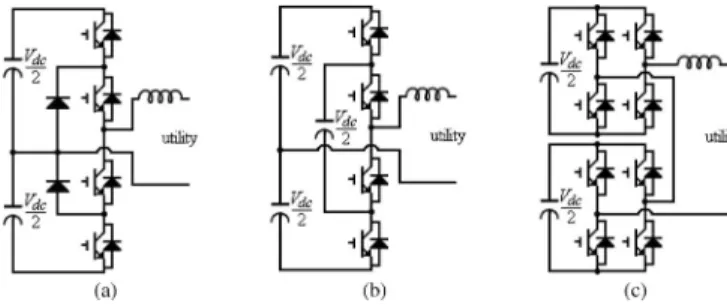
Fig. 1. Circuit configuration of conventional single-phase multilevel inverter. (a) Diode clamped. (b) Flying capacitor. (c) Cascade H-bridge.
the unipolar modulation is used. All power electronic switches operate in high switching frequency in both half-bridge and full-bridge inverters. The switching operation will result in switching loss. The loss of power electronic switch includes the switching loss and the conduction loss. The conduction loss depends on the handling power of power electronic switch. The switching loss is proportional to the switching frequency, voltage jump of each switching, and the current of the power electronic switches. The power efficiency can be advanced if the switching loss of the dc–ac inverter is reduced.
Multilevel inverter can effectively reduce the voltage jump of each switching operation to reduce the switching loss and increase power efficiency. The number of power electronic switches used in the multilevel inverter is larger than that used in the conventional half-bridge and full-bridge inverters. More-over, its control circuit is more complicated. Thus, both the performance and complexity should be considered in designing the multilevel inverter [8], [9]. However, interest in the multi-level inverter has been aroused due to its advantages of better power efficiency, lower switching harmonics, and a smaller fil-ter inductor compared with the conventional half-bridge and full-bridge inverters.
The conventional single-phase multilevel inverter topologies include the diode-clamped, the flying capacitor, and the cascade H-bridge types [10]–[15], as shown in Fig. 1. Fig. 1(a) shows the basic configuration of a diode-clamped multilevel inverter. As can be seen, it is configured by two dc capacitors, two diodes, and four power electronic switches. Two diodes are used to con-duct the current loop, and four power electronic switches are used to control the voltage levels. The output voltage of the basic diode-clamped multilevel inverter has three levels. The voltage difference of each level is Vdc/2 (the voltage on a
ca-pacitor). Since the voltages of two dc capacitors are used to form the voltage level of the multilevel inverter, the voltages of these two dc capacitors must be controlled to be equal. The control for balancing these two dc capacitors is very important 0885-8969/$31.00 © 2013 IEEE
258 IEEE TRANSACTIONS ON ENERGY CONVERSION, VOL. 28, NO. 2, JUNE 2013
in controlling the diode-clamped multilevel inverter, and it is very hard under the light load [16]–[19]. If the five-level output voltage is expected, extra two diodes and four power electronic switches are required [11], [20]. Fig. 1(b) shows the circuit con-figuration of a basic flying capacitor multilevel inverter. As can be seen, it is configured by three dc capacitors and four power electronic switches. The voltage on each dc capacitor is con-trolled to be Vdc/2, and the output voltage of the basic flying
capacitor multilevel inverter has three levels. The voltage differ-ence of each level is also Vdc/2 (the voltage on a dc capacitor).
These three dc capacitors must be controlled for maintaining their voltages to be Vdc/2 in the charge and discharge processes.
Therefore, its control circuit is more complicated. If five-level output voltage is required, an extra dc capacitor and four power electronic switches are required [11], [13], [14]. Fig. 1(c) shows the circuit configuration of the basic cascade H-bridge multi-level inverter [8]–[11], [15], [21]. As can be seen, it is config-ured by two full-bridge inverters connected in cascade. The dc bus voltage of each full-bridge inverter is Vdc/2, and the
out-put voltage of each full-bridge inverter can be controlled to be
Vdc/2, 0, and−Vdc/2. Thus, the voltage levels of the output
volt-age of the cascade full-bridge multilevel inverter are Vdc, Vdc/2,
0, −Vdc/2, and−Vdc. This topology has advantages of fewer
components being required compared with other multilevel in-verters under the output voltage with the same levels, and its hardware circuit can be modularized because the configuration of each full bridge is the same. However, this topology has the disadvantages that two independent dc voltage sources are required.
In this paper, a five-level inverter is developed and applied for injecting the real power of the renewable power into the grid. This five-level inverter is configured by two dc capacitors, a dual-buck converter, a full-bridge inverter, and a filter [22]. The five-level inverter generates an output voltage with five levels and applies in the output stage of the renewable power gen-eration system to generate a sinusoidal current in phase with the utility voltage to inject into the grid. The power electronic switches of the dual-buck converter are switched in high fre-quency to generate a three-level voltage and balance the two in-put dc voltages. The power electronic switches of the full-bridge inverter are switched in low frequency synchronous with the utility to convert the output voltage of the dual-buck converter to a five-level ac voltage. Therefore, the switching power loss, harmonic distortion, and electromagnetic interference (EMI) caused by the switching operation of power electronic devices can be reduced, and the control circuit is simplified. Besides, the capacity of output filter can be reduced. A hardware prototype is developed to verify the performance of the developed renewable power generation system.
II. CIRCUITCONFIGURATION
Fig. 2 shows the circuit configuration of the five-level inverter applied to a photovoltaic power generation system. As can be seen, it is configured by a solar cell array, a dc–dc converter, a five-level inverter, two switches, and a digital signal processor (DSP)-based controller. Switches SW1and SW2are placed
be-tween the five-level inverter and the utility, and they are used to disconnect the photovoltaic power generation system from the utility when islanding operation occurs. The load is placed between switches SW1 and SW2. The output of the solar cell
array is connected to the input port of the dc–dc converter. The output port of the dc–dc converter is connected to the five-level inverter. The dc–dc converter is a boost converter, and it per-forms the functions of maximum power point tracking (MPPT) and boosting the output voltage of the solar cell array. This five-level inverter is configured by two dc capacitors, a dual-buck converter, a full-bridge inverter, and a filter. The dual-dual-buck converter is configured by two buck converters. The two dc ca-pacitors perform as energy buffers between the dc–dc converter and the five-level inverter. The output of the dual-buck converter is connected to the full-bridge inverter to convert the dc voltage to ac voltage. An inductor is placed at the output of the full-bridge inverter to form as a filter inductor for filtering out the high-frequency switching harmonic generated by the dual-buck converter.
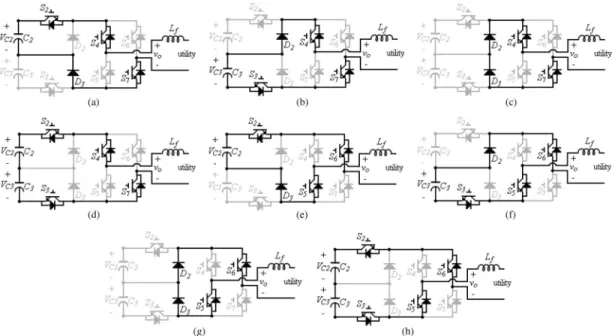
III. OPERATIONPRINCIPLE OFFIVE-LEVELINVERTER The operation of this five-level inverter can be divided into eight modes. Modes 1–4 are for the positive half-cycle, and modes 5–8 are for the negative half-cycle. Fig. 3 shows the operation modes of five-level inverter. As can be seen, the power electronic switches of the full-bridge inverter are switched in low frequency and synchronously with the utility voltage to convert the dc power into ac power for commutating. As seen in Fig. 3(a)–(d), the power electronic switches S4and S7 are in
the ON state, and the power electronic switches S5 and S6 are
in the OFF state during the positive half-cycle. On the contrary, the power electronic switches S4 and S7 are in the OFF state,
and the power electronic switches S5and S6are in the ON state
during the negative half-cycle. Since the dc capacitor voltages
VC 2and VC 3are balanced by controlling the five-level inverter,
the dc capacitor voltages VC 2 and VC 3 can be represented as
follows:
VC 2= VC 3 =
1
2Vdc. (1)
The operation modes of this five-level inverter are stated as follows.
Mode 1: Fig. 3(a) shows the operation circuit of mode 1.
The power electronic switch of the dual-buck converter S2 is
turned ON and S3is turned OFF. DC capacitor C2is discharged
through S2, S4, the filter inductor, the utility, S7, and D3 to
form a loop. Both output voltages of the dual-buck converter and five-level inverter are Vdc/2.
Mode 2: Fig. 3(b) shows the operation circuit of mode 2.
The power electronic switch of the dual-buck converter S2 is
turned OFF and S3is turned ON. DC capacitor C3is discharged
through D2, S4, the filter inductor, the utility, S7, and S3to form
a loop. Both output voltages of the dual-buck converter and five-level inverter are Vdc/2.
Mode 3: Fig. 3(c) shows the operation circuit of mode 3. Both
SHEN et al.: FIVE-LEVEL INVERTER FOR RENEWABLE POWER GENERATION SYSTEM 259
Fig. 2. Circuit configuration of the developed photovoltaic power generation system.
Fig. 3. Operation modes of the five-level inverter. (a) Mode 1. (b) Mode 2. (c) Mode 3. (d) Mode 4. (e) Mode 5. (f) Mode 6. (g) Mode 7. (h) Mode 8.
are turned OFF. The current of the filter inductor flows through the utility, S7, D3, D2, and S4. Both output voltages of the
dual-buck converter and five-level inverter are 0.
Mode 4: Fig. 3(d) shows the operation circuit of mode 4. Both
power electronic switches S2and S3of the dual-buck converter
are turned ON. DC capacitors C2and C3are discharged together
through S2, S4, the filter inductor, the utility, S7, and S3to form
a loop. Both output voltages of the dual-buck converter and five-level inverter are Vdc.
Modes 5–8 are the operation modes for the negative half-cycle. The operations of the dual-buck converter under modes 5–8 are similar to that under modes 1–4, and the dual-buck converter can also generate three voltage levels Vdc/2, Vdc/2, 0,
and Vdc, respectively. However, the operation of the full-bridge
inverter is the opposite. The power electronic switches S4 and
S7are in the OFF state, and the power electronic switches S5and
S6are in the ON state during the negative half-cycle. Therefore,
the output voltage of the five-level inverter for modes 5–8 will be−Vdc/2,−Vdc/2, 0, and−Vdc, respectively.
Considering operation modes 1–8, the full-bridge inverter converts the dc output voltage of the dual-buck converter with three levels to an ac output voltage with five levels which are
Vdc, Vdc/2, 0,−Vdc/2, and−Vdc.
The operation of power electronic switches S2and S3should
guarantee the output voltage of the dual-buck converter is higher than the absolute of the utility voltage. The waveforms of output voltage of five-level inverter and utility voltage are shown in Fig. 4.
Due to the operation of full-bridge inverter, the voltage and current in the dc side of full-bridge inverter are their absolute values of the utility voltage and the output current of the five-level inverter. When the absolute of the utility voltage is smaller than Vdc/2, the output voltage of the dual-buck converter should
change between Vdc/2 and 0. Accordingly, the power electronics
of five-level inverter is switched between modes 1 or 2, and mode 3 during the positive half-cycle. On the contrary, the power electronics of five-level inverter is switched between modes 5 or 6, and mode 7 during the negative half-cycle. One of the power
SHEN et al.: FIVE-LEVEL INVERTER FOR RENEWABLE POWER GENERATION SYSTEM 265
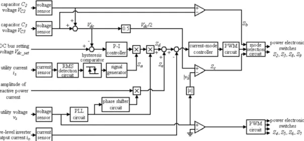
Fig. 17. Control block diagram of five-level inverter with the function of supplying reactive power.
62109-2 standard [26], the displace power factor must be higher than 0.95 and the reactive power is not required to be controlled if the dc–ac inverter capacity is smaller than 3.68 kVA. Since the capacity of the prototype in this paper is 1.2 kW, the dc– ac inverter generates ac power with the unity power factor is acceptable. If the five-level inverter must supply reactive power to the utility, two power electronic switches must replace the diodes D2and D3. So, the circuit configuration of the developed
photovoltaic power generation system shown in Fig. 2 must be changed to Fig. 16. Besides, a reactive power control loop must be added in the control circuit of five-level inverter shown in Fig. 6. Therefore, the control block diagram of five-level inverter must be changed to Fig. 17.
The switching operations of the replaced power tronic switches are complementary to those of power elec-tronic switches S2 and S3, respectively. Accordingly, the
five-level inverter can supply active power and reactive power simultaneously.
VII. CONCLUSION
A photovoltaic power generation system with a five-level in-verter is developed in this paper. The five-level inin-verter can perform the functions of regulating the dc bus voltage, convert-ing solar power to ac power with sinusoidal current and in phase with the utility voltage, balancing the two dc capacitor voltages, and detecting islanding operation. The experimental results ver-ify the developed photovoltaic power generation system, and the five-level inverter achieves the expected performance.
REFERENCES
[1] D. Puyal, L. A. Barragan, J. Acero, J. M. Burdio, and I. Millan, “An FPGA-based digital modulator for full- or half-bridge inverter control,”
IEEE Trans. Power Electron., vol. 21, no. 5, pp. 1479–1483, Sep. 2006.
[2] O. Lopez, F. D. Freijedo, A. G. Yepes, P. Fernandez-Comesaa, J. Malvar, R. Teodorescu, and J. Doval-Gandoy, “Eliminating ground current in a transformerless photovoltaic application,” IEEE Trans. Energy Convers., vol. 25, no. 1, pp. 140–147, Mar. 2010.
[3] B. R. Lin and C. L. Huang, “Implementation of a Shunt-series compen-sator for nonlinear and voltage sensitive load,” in Proc. IEEE Power
Electron. Motion Control Conf., 2006, pp. 1–5.
[4] U. S. Selamogullari, D. A. Torrey, and S. Salon, “A systems approach for a stand-alone residential fuel cell power inverter design,” IEEE Trans.
Energy Convers., vol. 25, no. 3, pp. 741–749, Sep. 2010.
[5] J. Gafford, M. Mazzola, J. Robbins, and G. Molen, “A multi-kilowatt high-frequency ac-link inverter for conversion of low-voltage dc to utility power voltages,” in Proc. IEEE Power Electron. Spec. Conf., 2008, pp. 3707– 3712.
[6] T. H. Ai, J. F. Chen, and T. J. Liang, “A random switching method for HPWM full-bridge inverter,” IEEE Trans. Ind. Electron., vol. 49, no. 3, pp. 595–597, Jun. 2002.
[7] C. Y. Chen, Y. H. Lin, J. F. Chen, and R. L. Lin, “Design and implemen-tation of DSP-based voltage frequency conversion system,” in Proc. Int.
Symp. Comput. Commun. Control Autom., May 2010, pp. 435–438.
[8] M. Chithra and S. G. B. Dasan, “Analysis of cascaded H bridge multilevel inverters with photovoltaic arrays,” in Proc. Int. Conf. Emerging Trends
Elect. Comput. Technol., Mar. 2011, pp. 442–447.
[9] N. Yousefpoor, S. H. Fathi, N. Farokhnia, and S. H. Sadeghi, “Application of OHSW technique in cascaded multi-level inverter with adjustable dc sources,” in Proc. Int. Conf. Electric Power Energy Convers. Syst., 2009, pp. 1–6.
[10] S. De, D. Banerjee, K. Siva Kumar, K. Gopakumar, R. Ramchand, and C. Patel, “Multilevel inverters for low-power application,” IET Power
Electron., vol. 4, no. 4, pp. 384–392, Apr. 2011.
[11] A. Nami, F. Zare, G. Ledwich, A. Ghosh, and F. Blaabjerg, “Comparison between symmetrical and asymmetrical single phase multilevel inverter with diode-clamped topology,” in Proc. IEEE Power Electron. Spec. Conf., Jun. 2008, pp. 2921–2926.
[12] E. Ozdemir, S. Ozdemir, and L. M. Tolbert, “Fundamental-frequency-modulated six-level diode-clamped multilevel inverter for three-phase stand-alone photovoltaic system,” IEEE Trans. Ind. Electron., vol. 56, no. 11, pp. 4407–4415, Nov. 2009.
[13] A. Nami, F. Zare, A. Ghosh, and F. Blaabjerg, “A hybrid cascade converter topology with series-connected symmetrical and asymmetrical diode-clamped H-Bridge cells,” IEEE Trans. Power Electron., vol. 26, no. 1, pp. 51–65, Jan. 2011.
[14] A. A. Boora, A. Nami, F. Zare, A. Ghosh, and F. Blaabjerg, “Voltage-sharing converter to supply single-phase asymmetrical four-level diode-clamped inverter with high power factor loads,” IEEE Trans. Power
Elec-tron., vol. 25, no. 10, pp. 2507–2520, Oct. 2010.
[15] P. Samuel, R. Gupta, and D. Chandra, “Grid interface of wind power with large split-winding alternator using cascaded multilevel inverter,” IEEE
Trans. Energy Convers., vol. 26, no. 1, pp. 299–309, Mar. 2011.
[16] O. Bouhali, B. Francois, E. M. Berkouk, and C. Saudemont, “DC link capacitor voltage balancing in a three-phase diode clamped inverter con-trolled by a direct space vector of line-to-line voltages,” IEEE Trans.
266 IEEE TRANSACTIONS ON ENERGY CONVERSION, VOL. 28, NO. 2, JUNE 2013
[17] G. P. Adam, S. J. Finney, A. M. Massoud, and B. W. Williams, “Capacitor balance issues of the diode-clamped multilevel inverter operated in a quasi two-state mode,” IEEE Trans. Ind. Electron., vol. 55, no. 8, pp. 3088–3099, Aug. 2008.
[18] G. P. Adam, S. J. Finney, B. W. Williams, and M. T. Mohammed, “Two-level operation of a diode-clamped multi“Two-level inverter,” in Proc. IEEE Int.
Symp. Ind. Electron., Jul. 2010, pp. 1137–1142.
[19] C. Xia, X. Gu, T. Shi, and Y. Yan, “Neutral-point potential balancing of three-level inverters in direct-driven wind energy conversion system,”
IEEE Trans. Energy Convers., vol. 26, no. 1, pp. 18–29, Mar. 2010.
[20] X. Ruan, B. Li, Q. Chen, S. C. Tan, and C. K. Tse, “Fundamental consider-ations of three-level dc–dc converters: Topologies, analyses, and control,”
IEEE Trans. Circuits Syst. I: Reg. Papers, vol. 55, no. 11, pp. 3733–3743,
Dec. 2008.
[21] F. Khoucha, M. S. Lagoun, A. Kheloui, and M. El Hachemi Benbouzid, “A comparison of symmetrical and asymmetrical three-phase H-bridge multilevel inverter for DTC induction motor drives,” IEEE Trans. Energy
Convers., vol. 26, no. 1, pp. 64–72, Mar. 2011.
[22] H. D. Sun, M. Y. Park, J. H. Park, H. G. Kim, T. W. Chun, and E. C. Nho, “Novel H-bridge multi-level inverter with dc-link switches,” in Proc. IEEE
Int. Conf. Power Electron. ECCE Asia, 2011, pp. 1734–1741.
[23] J. M. Shen, H. L. Jou, and J. C. Wu, “Grid-Connected power converter with islanding detection and active power filter functions,” in Proc. IEEE
Int. Symp. Power Electron. Distrib. Generation Syst., Jun. 2010, pp. 501–
506.
[24] G. J. Yu, Y. S. Jung, J. Y. Choi, and G. S. Kim, “A novel two-mode MPPT control algorithm based on comparative study of existing algorithms,”
Solar Energy, vol. 76, no. 4, pp. 455–463, 2004.
[25] IEEE Recommended Practice for Utility Interface of Photovoltaic (PV)
Systems, IEEE Std 929-2000, 2000.
[26] Safety of Power Converters for Use in Photovoltaic Power Systems—Part
2: Particular Requirements for Inverters, IEC 62109-2, Ed.1, 2011.
Jia-Min Shen (M’08) was born in Tainan, Taiwan, in
1982. He received the B.S.E.E. degree, the M.S.E.E. degree, and the Ph.D.E.E. degree from National Kaohsiung University of Applied Sciences, Kaoh-siung, Taiwan in 2005, 2007, and 2012, respectively.
He is currently with the R&D Department, Ablerex Electronics Company, Kaohsiung, Taiwan. His re-search interests include power electronics applica-tions and DSP control.
Hurng-Liahng Jou (M’99) was born in Taiwan, in
1959. He received the B.S.E.E. degree from Chung Yuan University, Jonglih, Taiwan, in 1982, and the M.S.E.E degree and the Ph.D.E.E. degree from Na-tional Cheng Kung University, Tainan, Taiwan, in 1984 and 1991, respectively.
He is currently a Professor in the Department of Electrical Engineering of National Kaohsiung Uni-versity of Applied Sciences, Kaohsiung, Taiwan. His research interests include power electronics applica-tions and power quality improvement.
Jinn-Chang Wu (M’07) was born in Tainan,
Tai-wan, in 1968. He received the Graduate degree from National Kaohsiung Institute of Technology, Kaohsiung, Taiwan, in 1988, and the M.S.E.E. and the Ph.D.E.E. degrees from National Cheng Kung University, Tainan, Taiwan, in 1992 and 2000, respectively.
He is currently an Associate Professor in the Department of Microelectronics Engineering, Na-tional Kaohsiung Marine University, Kaohsiung, Taiwan. His research interests include power qual-ity and power electronics applications.
Kune-Der Wu was born in Tainan, Taiwan, in 1954.
He received the B.S.E.E. degree from Tamkang Uni-versity, Taipei, Taiwan, in 1977, and the M.S.E.E. de-gree from National Cheng Kung University, Tainan, Taiwan, in 1980.
He is currently an Associate Professor in the De-partment of Electrical Engineering, National Kaohsi-ung University of Applied Sciences, KaohsiKaohsi-ung, Tai-wan. His research interests include power electronics applications and power quality improvement.