Materials Chemistry and Physics 49 ( 1997) 29-32
Growth and electron effective mass measurements of strained Si and
%94Ge0.06
on relaxed Si 0.62Ge0.38
buffers grown by rapid thermal
chemical vapor deposition
C.W. Liu a, V. Venkataraman b
a Nationai Taiwan Universily, Department of Electrical Engineering, Taipei. Taiwan
b Indian Institute of Science, Bangaiore, Dept. of Physics, Bangalore, India
Received 16 July 1996; revised 30 August 1996; accepted 30 August 1996
Abstract
We report the growth and the electron cyclotron resonance measurements of n-type Si/Sio,62Geo,38 and Si,,Ge o.os/Sio.62Geo.38 modulation- doped heterostructures grown by rapid thermal chemical vapor deposition. The strained Si and SiO,wGeO,O, channels were grown on relaxed %.&eo.38 buffer layers, which consist of 0.6 km uniform Si o.ezGe,.3, layers and 0.5 pm compositionally graded relaxed SiGe layers from 0 to 38% Ge. The buffer layers were annealed at 800°C for 1 h to obtain complete relaxation. A 75 A Si(SiGe) channel with a 100 A spacer and a 300 A 2 X 10” cm- 3 n-type supply layer was grown on the top of the buffer layers. The cross-sectional transmission electron microscope reveals that the dense dislocation network is confined to the buffer layer, and relatively few dislocations terminate on the surface. The plan- view image indicates the threading dislocation density is about 4X lo6 cme2. The far-infrared measurements of electron cyclotron resonance were performed at 4 K with the magnetic field of 4-8 T. The effective masses determined from the slope of the center frequency of the absorption peak versus applied magnetic field plot are 0.203m, and O.l93m, for the two dimensional electron gases in the Si and Sio,94Ge0,0s channels, respectively. The Si effective mass is very close to that of a two dimensional electron gas in an Si MOSFET (O.l98m,). The electron effective mass of Si0.94Geo,06 is reported for the first time and is about 5% lower than that of pure Si.
Keywords: Graded relaxed buffer; SiGe; Cyclotron resonance; Electron effective mass
1. Introduction
Recently, there has been remarkable progress in SiGe tech- nology. The fr (cutoff frequency) andf,, (maximum fre- quency of oscillation) of Si/SiGe heterojunction bipolar transistors (HBT) have reached 117 GHz [ l] and 160 GHz
[ 21, respectively. This possibly offers S&based KS with low cost and high speed to wireless communication markets. Moreover, the electron mobility and hole mobility of 5.2X lo5 [3] and 5.5 X lo4 cm2 V-’ s-l [4], respectively, have been demonstrated in modulation-doped structures, which provide perfect material systems to study the physics of two dimensional hole/electron gases. To study the carrier transport in the H3T devices or in the two dimensional carrier gases, the carrier effective masses have to be determined. The hole effective masses of strained SiGe on Si have been reported by several workers, but some controversy is not yet resolved [ 51. The effective mass of two dimensional elec-
0254-0584/97/$17.00 0 1997 Elsevier Science S.A. All rights reserved
PIISO254-0584(96)01905-O
trons in Si has been studied in the Si MOSFET [ 61 structures and in the strained-Si/relaxed-SiGe heterostructures [ 71. However, to the best of our knowledge, there is no report of electron effective masses of SiGe in any structures.
The cyclotron resonance (CR) technique has been widely used to measure the electron effective masses in semicon- ductors. Because of the lack of high-quality bulk SiGe mate- rials, we have to perform the CR measurements in SiGe epilayers on Si substrates. Owing to the small conduction band offset [ 8 ] between compressively strained SiGe and relaxed Si, electron confinement in strained-SiGe/relaxed-Si heterostructures is limited and CR cannot be performed. Theoretical calculations [S] and experimental results [ 31 showed that there was significant conduction band offset in tensilely strained-sir -,Ge,/relaxed-Sir -,Ge, heterostructu- res as long as x < y. We have, therefore, fabricated such het- erostructures by rapid thermal chemical vapor deposition (RTCVD) and investigated the electron effective masses in such structures.
30 C. W. Liu, V. Venkataraman / Muterials Chemistry and Physics 49 (1997) 29-32
2. Growth
All samples used in this study were grown by RTCVD. The growth system consists of a cold wall quartz tube with a loadlock. The wafer is supported on a quartz stand and heated by tungsten halogen lamps. The wafer temperature is accu- rately determined by monitoring infrarid transmission through the wafer. The growth pressure is 6 Torr and the gases used are dichlorosilane (SiCl,H,) for silicon and ger- mane mixture (0.8% GeH4 in H,) for germanium. The n- type doping is accomplished by adding phosphine mixture (70 ppm PH, in HZ) into the gas mixture. Details of the growth system can be found in Ref. [ 91. The relaxed
Si0.62Ge0.38 layers were grown on 100 mm lightly-doped p-
type ( 100) Si wafers at 625°C after an initial high temperature (1000°C) cleaning in hydrogen. A compositionally graded buffer was used to reduce the threading dislocation density of relaxed Sio.,,Geo,3s layers. The Ge content of the buffer layer was graded form 0% at the Si substrate to 38% at the top of the graded layer over a distance of = 0.5 km, and then a uniform Si0,62Ge0,38 layer with the thickness of ~0.6 pm was deposited on the graded layer. Before the growth of active layers (electron channels), the structure was annealed in situ for 1 h at 800°C to ensure complete relaxation. X-ray diffrac- tion shows the (400) SiGe peak of the 1 h annealed samples (8OO”C, in furnace with forming gas flow) shifts toward the (400) peak of Si substrate by 0.1” compared with the as- grown sample with the same buffers, but not annealed. No more shift is observed for the same sample annealed for another 9 h at 800°C. This indicates 1 h annealing time is sufficient at 800°C to relax the as-grown film completely. Modulation-doped structures were grown to confine electrons in the Si or Sio.94Geo.os channels. A 75 A tensiley strained Si or Sio,a4Geo,a, channel was grown on the buffer, followed by an undoped 100 A Si,,,,Ge0,38 relaxed spacer and a heavily phosphorus-doped 3OO.A Sio,62Ge0,,, supply layer. The dop- ing level in the supply layer was approximately = 2 X 10” cme3, estimated by spreading resistance meas- urements. A schematic cross-section of the entire structure is shown in Fig. 1.
n+ - Si o,62 Geo.3~ cap - 300 .k (relaxed)
i - Sin.62 Ge0.38 spacer (relaxed)
---SDEG ---
i - Sil-,Ge, channel N 75 A (strained)
in-situ annealed at 800°C for 1 hr
uniform relaxed Si 0.62 Ge 0.38 - 0.6 fml
graded SiGe buffer 0 - 38 % N 0.5 p’m
p-type Si substrate
Fig, 1. Sample structures for effective mass measurements. The samples
consist of 100 A spacers, =2X lOI crne3 n-type caps, and SiI-,Ge,chan-
nels (0% or 6%) grown at 625°C.
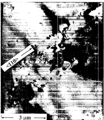
Fig. 2. A plan-view TEM image of a relaxed buffer layer. A defect band clearly exists along the (1 IO) direction.
The threading dislocation density was characterized by plan-view transmission electron microscope (TEM) . The average separation between threading dislocations is about 5 pm, indicating the threading dislocation density is around 4 X lo6 cm-*. However, the threa.ding defects are not distrib- uted uniformly within the same [sample, and ‘defect bands’ exist at the surface with a th:reading defect density of
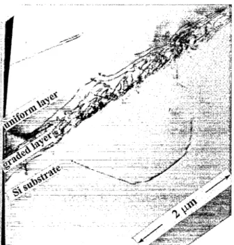
= 10’ cm-* (Fig. 2). The defect bands are aligned along the misfit dislocation directions, i.e. ( 110) directions. The origin of these defect bands is not clear at this point. The cross- sectional TEM (Fig. 3) shows th.at a dense network of misfit dislocations is confined in the graded buffers. Some dislo- cations penetrate deeply into the Si substrates. This is contra- dictory to Matthews and Blakeslee’s theory [ IO], in which they assumbd the dislocations were confined in the epilayers, because of relatively small thickness of the epilayers as com- pared to substrates. Similar resulrs were also observed in the samples prepared by UHV (ultra high vacuum) CVD and a modified Frank-Read source [ 1 I.1 was proposed to explain this phenomenon. Relatively few dislocations terminated on the surface. The uppermost (active) layer appears largely dislocation free.
3. Cyclotron measurements
To measure the electron concentration and mobility, Hall measurements were carried out by using Van der Pauw geom- etry with Au:Sb contacts. A 50 A Au layer, followed by
1500 A Au:Sb alloys (0.6-24% !Sb), and a 1000 A Au layer was thermally evaporated and lifted off to form contact pads.
C. W. Liu, V. Venkatararnarl/ Materials Chemistry and Physics 49 (1997) 29-32 31
Fig. 3. A cross-sectional TEM image of a relaxed buffer layer. The dense network of dislocations is confined in the graded buffer layers and the top of uniform layer is relatively dislocation free. Some dislocations penetrate into the Si substrate.
Owing to the poor adhesion of Sb to the SiGe surface, the initial Au layer is crucial to avoid fall-off of the contact pads. Finally, the contacts were annealed at 350-4OO”C for lo-
15 min to form ohmic contacts down to 10 K. Both samples showed typical modulation-doped behavior. The mobility increases monotonically for both samples with decreasing temperature, reaching 20 000 and 6420 cm2 V- ’ s - ’ at 10 K for Si and Si,,BdGeO.OG channels, respectively. The carrierden- sity decreases with decreasing temperature and reaches 1.2X 10¹² and 1.4 X lOI cme2 at 10 K for Si and Si0.94Ge0.0s channels, respectively. Some parallel conduction was observed for the Si,,94Ge0.0s sample, but was removed after etching the supply layer. The magnetotransport experiments have been performed in similar structures and showed well- defined Shubnikov-de Hass oscillation in the longitudinal resistance and quantized Hall plateaux in the transverse resis- tance [ 12].
The Si and Sio.94Geo.os layers grown on relaxed Si0.62GeD.38 buffers yield the tensile strain in the channels, which breaks the sixfold degeneracy in the bulk materials. The twofold conduction valleys along the growth direction is lower in energy than the fourfold conduction valleys perpendicular to the growth direction. At low temperature (4 K) , the electrons in these two samples occupied the lowest valleys (confirmed by magnetotransport experiments [ 121) and the effective mass measured in the two dimensional electron gas is the transverse electron mass (light mass). Fig. 4 shows the nor- malized transmission spectra (T(B) /T(O)) at 4 K with applied magnetic fields from 4 to 8 T for the two dimensional electron gas in the Si channel, The electron effective mass in Si can be determined by the slope of the plot of absorption peak frequency (in the unit of cm- ’ ) as a function of mag-
L 1.4 1 Si Channel 1.3 - ‘.’ - 4T 5-r 6T7-r 8T 4 "70 I 20 30 40 50 60 I Frequency (cm-‘)
Fig. 4. Normalized cyclotron resonance spectra at 4 K of the Si channel with applied magnetic field from 4 to 8 T.
oy , I I I I I
0 2 4 6 8
Magnetic field (T)
Fig. 5. Absorption peak frequency as a function of applied magnetic field for Si and Si0,,Geo.06 channels. From the slopes, the effective masses of the two dimensional electron gases are determined.
netic field (Fig. 5), using w, = eB/m"c, where w, is the absorption frequency, e is the electron charge, B is the applied magnetic field, m* is the effective mass, and c is the speed of light. The average effective mass is 0.203m,, slightly higher than that of the two dimensional electron gas in Si MOSFETs
[6] (O.l98m,) with an electron concentration of 1 X 1Ol2 cmm2 and that of Si/SiGe modulation-doped struc- tures [7] (O.l95m,) with electron concentrations of 1.6- 3.5 X 10” cmW2, This might be due to the higher electron
concentration in our sample, because previous studies [ 6,7] showed the electron effective mass of Si increases as the carrier concentration increases. Note that due to broad line- width ( = 12 cm-‘), the estimated error bar is 5% in our experiments. It is possible that the slightly higher value of electron effective mass in our experiments is due to theuncer- tainty in the measurements.
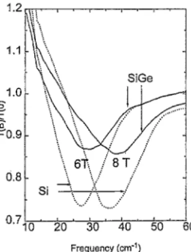
The absorption spectra of the two dimensional electron gas in the S&.d%o~ channel are shown in Fig. 6 at 4 K with magnetic fields of 6 and 8 T. The effective mass of Si0,94Ge0.0, obtained from the plot of absorption peak as a function of applied-field is O.l93m,. Compared to the absorption spectra
C. W. Liu, V. Venkataraman / Materials Chemistry and Physics 49 (1997) 29-32
Frequency (cm-‘)
Fig. 6. Normalized cyclotron resonance spectra at 4 K of the SiO.saGea.os channel with applied magnetic fields of 6 and 8 T. Compared with the absorption spectra of Si samples at 6 and 8 T (dotted line), the absorption spectra of Si,,g,Ge,,O, consistently shift about 5% of the center frequency toward the high frequency side.
of Si samples at 6 and 8 T (Fig. 6)) the absorption spectra of Si,,,,Ge0,06 consistently shift about 5% of the center fre- quency toward high frequency side. Therefore, we conclude that electron effective mass (0.193~~~) of Si0.94Ge,,0s is about 5% lower than that of Si (0.203m,), despite of the error bar of measurements. Two effects may be responsible to the lower electron effective mass of Sio,94Geo,oS: the different Ge content in the channels (0 versus 0.06) and the different strain (0.04 X 0.38 versus 0.04 X 0.32,0.04 is the misfit between Si
and Ge) due to different lattice constant between the Si ( Si,,94Ge0.06) channel and the Si,,,Ge,.,, relaxed buffer. Although the strain effect has been theoretically studied in some direct valleys [ 131, it is still not known in indirect conduction valleys. The change of effective mass solely due to the Ge content as in the bulk SiGe can not be determined.
4. Summary
We have successfully fabricated the strained Si( Sio,94Ge0,0s) /relaxed Si0,62Ge0,38 modulation-doped
structures with low threading dislocation densities and high electron densities in Si and Si0,94Ge0,0s channels. The cyclo- tron resonance measurements indicate the electron effective mass of strained Si,,94Ge0,0s on relaxed Si0,62Ge0,38 buffer is O.l93m,, which is about 5% lower than that of strained Si on the same buffer.
Acknowledgements
The wafer supply from Professor J.C. Sturm (Princeton University), the CR assistance of Dr S.H. Song (Princeton University), and the TEM assistance of Dr J.T. McGinn (David Sarnoff Research Center) are gratefully appreciated. One of the authors (C.W. Liu) would like to thank the support of National Science Council of ROC under contract No. 85 2215-E-005-002 for publishing this paper.
References
[l] E. Crabbe, B.S. Meyerson, J.M.C. Stork and D.L. Harame, Teclz. Dig. Int. Electron. Dev. Meet., IEEE, Piscataway, N.J., U.S.A., 1993, p. 83. [2] A. Schuppen, U. Erben, A. Gruhle, H. Kibble, H. Schumacher and U. Konig, Tech. Dig. Int. Electron. Dev. Meet., IEEE, Piscataway, N.J.,
U.S.A., 1995, p. 743.
[3] K. Ismail, M. Arafa, K.L. Saenger, J1.0. Chu and B.S. Meyerson,Appl.
Phys. Lett., 66 (1995) 1077.
[4] Y.H. Xie, Don Moroe, E.A. Fitzgerald, P.J. Silverman, F.A. Thiel and G.P. Watson, Appl. Phys. Letf,, 63 (1993) 2263.
[5] T.E. Whall, A.D. Plews, N.L. Mattey and E.H.C. Parker, Appl. Pkys.
L&r., 65 (1994) 3362.
[6] J.P. Kotthaus, G. Abstreiter, J.F. Koch and R. Ranvaud, Phys. Rev.
Lat., 34 (1975) 151.
[7] S.Q. Murphy, 2. Schlesinger, S.F. Nelson, J.O. Chu and B.S. Meyerson, Appl. Pkys. L&t., 63 (1993) 222.
[8] C.G. van de Walle and R. Martin, Pkys. Rev. B, 34 (1986) 5G21. [9] JC, Sturm, P.V. Schwartz, E.J. Prinz and H. Manoharan, J. Vat. Sci.
Tecknol. B, 9 (1991) 2011.
[lo] J.W. Matthews and A.E. Blakeslee, J. Cryst. Growth, 27 (1974) 118. [ 1 l] F.K. LeGoues, B.S. Meyerson, J.F. Morar and P.D. Kirchner, J. Appl.
Pkys., 71 (1992) 4230.
[12] V. Venkataraman, C.W. Liu and J.C. Sturm, J. Vuc. Sci. Tech. B, 11
( 1993) 1176.