利用脈衝雷射濺鍍光電半導體硒化鎵於不同基板之研究
57
0
0
全文
(2) material, such as GaSe, without strong bonding allows the possibility to remove the constraint of lattice mismatch between the 2D thin film and three-dimensional (3D) substrate. More recently the growth of a high quality thin film of GaSe is virtually always obtained by molecular beam epitaxy (MBE). Reflection high-energy electron diffraction, x-ray photoelectron spectroscopy, and transmission electron microscopy were used to study the interface reaction and demonstrate that layered compound GaSe on 3D silicon substrate belongs to VdEW epitaxy. Although MBE is powerful for fabricating GaSe thin films, the pulsed laser deposition (PLD) method is reported in this study. In our group, the growths of GaSe thin films have been developed for two years. The pretty good quality of GaSe thin films were fabricated and their structural and optical properties, such as x-ray diffraction, atomic force microscopy, photoluminescence and Raman spectra, were demonstrated. According to structural analysis, a grain size of about 5720Å is obtained which is similar to the result of the film grown by MBE in ref.12 and even better than that in ref.13. High quality of GaSe thin films were already obtained in our research group.. 1.2. Research Motivation In the passed two years, our group makes efforts in fabricating high quality thin. films of GaSe.14,15) A large number of experimental parameters were achieved completely and their characteristics of as-grown thin films were demonstrated. Besides, the behaviors of annealing process were also observed before. But the growth modes of GaSe thin film, using PLD method, do not understand clearly. In addition, the thickness of their sample is almost larger than 80nm. Thus in our. 2.
(3) experiment, the GaSe thin films were deposited at the thickness below 80nm. It is attractive to understand when the films are thinner. Although, according to koma’s deduction, GaSe thin film should belong to VdEW epitaxy and several research groups confirm it by using MBE system. The growth mechanism of PLD is different from MBE. Compared to the MBE technique, PLD does not only involve the physical process between the target material and the impacted high-power pulsed radiation while laser ablation, 16) but also the formation of plasma plume with high energetic species and even transfer of the ablated material through the plasma plume onto the heated substrate surface. However, there are different sizes of different ionic or molecular clusters in the plume during depositing onto the substrate. It makes huge variation between growth system of MBE and PLD. In this thesis, we try to find the growth behavior by PLD technique and this will give us more information to deal with the heterostructure formed by 2D materials on the 3D substrates. Experimentally, very thin films of GaSe could be prepared by controlling film growth deposition time on the substrate. Besides the growth mode of Gase thin film, we also want to verify how the lattice mismatches affect the film quality of GaSe during deposition process. Thus, three different kind of hexagonal- like substrate, Si (111), c-cut GaN, and Sapphire, were used and lattice mismatches between GaSe and these substrates are 2%, 15%, and 25.8%, respectively.. 1.3 The basic property of GaSe In III-VI compounds semiconductors, gallium selenide has a number of exciting properties for nonlinear optical applications and excellent review has been compiled by Fernelius.17,18,19) Light transmits this material in the range extending from 0.65 to. 3.
(4) 18 micrometer wavelength range and optical absorption coefficient remains below 1cm-1 throughout the transparency range. The high nonlinear optical coefficient and large birefringence are also reported.20) Therefore, GaSe could easily satisfy phase matching relations and hence has possibility for effectively converting input beams into its sum and difference frequencies. GaSe exist as a layered material with several polytypes designated as β, γ, δ and ε. A great deal of studies have made by several research groups to understand the polytypes in this compound. β and ε have been reported to have hexagonal structures with lattice parameter a=3.755Å and c=15.95Å which corresponds to a group P63 /mmc. The γ type structure is rhombohedral with space group R3m, and δ type GaSe is hexagonal with space group P63 mc. Most of the papers covered in this work deal with the ε type. Most of the work covered in the papers deal with the ε phase. The ε type GaSe is a negative uniaxial crystal (no >ne, where no and ne denote the refractive indices in the ordinary and extraordinary direction) with point group 6m2(D3h ) or 62m(Table1-2). Figure.1-1 shows structure of GaSe, and atomic configuration of GaSe layers. Its layer structure consists of four close-packed monoatomic sheets in the sequence Se-Ga-Ga-Se. The strong bounding between two sheets of the same layer is supposed to be covalent with some ionic contribution. But the bonds between the complete four- fold layer is believed to be essentially of the Vander Waal type. Fig. 1-1(a) shows a single layer of the GaSe which has sp3 bound and its formal electronic configuration is listed in Table 1-3. The bond between the Ga atoms is perpendicular to the plane of the sheet. These Ga-Ga dimmers are then connected together by the Se atoms whose forming bond length is 2.35Å and the bond length between the Se and the Ga atoms is 2.47Å. Figure 1-1 (b)-(d) show the unit cell is hexagonal with a lattice constant of a=3.755Å (Table1-1). The layer distance, which is 4.73 Å (from Se atom to Se atom) in thickness, interacts through a van der 4.
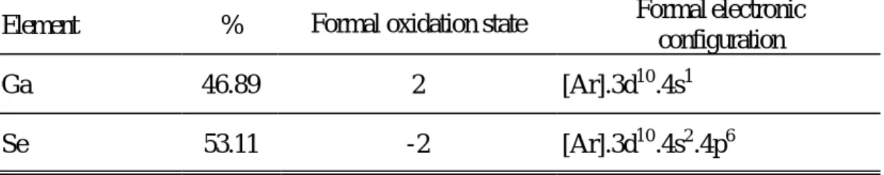
(5) Waals potential and the distance between Se atoms on different layers to be 3.0Å.. Table1-1 GaSe CRYSTAL DATA Crystal Symmetry. Hexagonal. Point Group. 62m. Lattice Constants (Å). a0 = 3.755 c0 = 15.95. Table 1-2 NONLINEAR OPTICAL PROPERTIES Laser damage threshold (MW/cm2 ). Indices of refraction at. 28. 1.06(μm) no 2.9082. at pulse duration (ns) 150. ne 2.5676. at wavelength (μm) 9.3. n0 2.8340. Nonlinearity (pm/V) 63. 5.3(μm). ne 2.4599 10.6(μm) no 2.8158 ne 2.4392. Phase matching angle for TypeⅠ SHG at 1.06μm, (deg). 14. Table 1-3 GaSe (density: 5.03g/cm3 ) Formal electronic configuration. %. Formal oxidation state. Ga. 46.89. 2. [Ar].3d10 .4s1. Se. 53.11. -2. [Ar].3d10 .4s2 .4p6. Element. 5.
(6) Chapter 2. 2.1. Theoretical background. Pulse Laser Deposition (PLD) Laser, as a source of pure energy in the form of monochromatic and coherent. photons, is enjoying ever increasing popularity in devise. In material science, lasers also play a significant role as a an active tool by coupling its radiation energy into the material being processed, leading to various application such as PLD(Pulsed Laser Deposition). Figure2-1 shows a schematic diagram of an experiment setup. A high -power laser is used as an external energy source to vaporize materials and to deposite thin films. A set of optical components is used to focus and raster the laser beam over the target surface. In general, the pulsed laser deposition is simple due to a few parameters need to be controlled during the growth process. The target used in PLD are small compared with the large size require ment for other sputtering techniques. It is quite easy to produce multi- layer films of different materials by rotating the target consistent of two materials. Besides, by controlling the number of pulses, a fine control of film thickness can be achieved. Thus a fast response in exploiting new material system is a unique feature of PLD among other deposition methods. The most important feature of PLD is that the stoichiometry of the target can be retained in the deposition films. This is the result of the extremely high heating rate of the target surface(~108 K/s) due to pulsed laser irradiation. It leads to the congruent evaporation of the target irrespective of the evaporation point of the constituent element or compounds of the target. And because of the high heating rate of the ablated materials, laser deposition of crystalline film demands a much lower temperature than other mentioned film 6.
(7) growth techniques. The principle of pulsed laser deposition, in contrast to the simplicity of the system set-up, is a very complex physical phenomenon. It does not only involve the physical precess of the laser- material interaction of the impact of high-power pulsed radiation on solid target, but also the formation plasma plasma with high energetic species and even the transfer of the ablated material through the plasma plume onto the heated substrate surface.16) Thus, the thin film formation precess in PLD generally can be divided into the following four stages. 1. Laser radiation interaction with the target. 2. Dynamic of the ablation materials. 3. Deposition of the ablation materials with the substrate. 4. Nucleation and growth of a thin film on the substrate surface. Each step in PLD is critical to the formation of high quality crystalline, stoichiometric, uniform and small surface roughness of thin film. In the first stage, the laser beam is focus onto the surface of target. At sufficiently high flux densities and short pulse duration, all elements in the target are rapidly heated up to their evaporation temperature. Materials are dissociated from the target surface and ablated out with stoichiometry as in the target. The instantaneous ablation rate is highly dependent on the fluorescence of the laser shining on the target. The ablation mechanism involve many complex physical phenomena such as collisional, thermal, and electronic excitation, exfoliation and hydrodynamics. During the second stage the emitted materials tend to move towards the substrate according to the laws of gas-dynamic and show the forward peaking phenomenon. The spot size of laser and temperature of plasma have significant effects on the deposition film uniformity. The target-to-substrate distance is another parameter that governs the angular spread of the ablation materials. 7.
(8) The third stage is important to determine the quality of the film. The ejected high-energy species impinge onto the substrate surface and may induce various type of damage to the substrate. These energetic species sputter some of the surface atoms and a collision region is formed between the incident flow and the sputtered atoms. Film grows after a thermalized region is formed. The region serves as a source for condensation of particles. When the condensation rate is higher then the rate of particles supplied by the sputtering, thermal equilibrium condition can be reached quickly and film grows on the substrate surface at the expenses of the direct flow of the ablation particles and the thermal equilibrum obtained. Nucleation-and-growth of crystalline films depends on many factors such as the material density, energy, ionization degree, and the type of the condensing material, as well as the temperature and the physico-chemical properties of the substrate. The two main thermodynamic parameters that determine to a great extent the growth mechanism are the substrate temperature T and the supersaturation m. m = kT • ln. R Re. (2-1). where k is the Boltzman constant , R is the actual deposition rate, and Re is the equilibrium value at temperature T. At the extremely high deposition rate in PLD, the plasma flux super-saturation may be reached, which is the small size of the nuclei (practically one atom) (Metev, 1989). The nucleation process depends on the interfacial energies between the three phases present-substrate, the condensing material and the vapor.. The minimum-energy. shape of a nucleus is like a cap. The critical size of the nucleus depends on the driving force (i.e. the deposition rate and the substrate temperature). And the crystalline film growth depends on the surface mobility of the adatom (vapor atoms). Normally, the adatom will diffuse through several atomic distances before sticking to. 8.
(9) a stable position within the newly formed film.. The surface temperature of the. substrate determines the adatom's surface diffusion ability. High temperature favors rapid and defect free crystal growth, whereas low temperature or large super-saturation crystal growth may be overwhelmed by energetic particle impingement, resulting in disordered or even amorphous structures. For the properties of the film, the stage of initial film growth up to the moment of substrate surface covering with a continuous layer is very important. When the time constants of filling the successive monolayers are known that it’s possible to determine the dependence on the experimental conditions of the mean film thickness, N (in number of mono-layers) at the moment of 99% covered substrate (Kashchiev, 1978). Physically, N can be interpreted as the “mean thickness” at which a growing thin discontinuous film reaches continuity. For the concrete model of PLD, N has been found to be given :(Metev and Meteva, 1989) 1/ 3. vN N = 0.5 0 R . − 3E des + 2 Esd ∗ exp 3kT . (2-2). where v being the adatom vibrational ferq. ; N0 is the density of adsorptions on the substrate; R is the actual deposition rate; Edes, the activation energy for adsorb-atom desorption; and Esd, the activation energy of adatom surface diffusion. The R-T-dependence of N has a useful presentation that may be called a growth diagram (Kashchiev, 1978). That is in lnR versus 1/T coordinates we can draw lines of equal mean film thickness (at the moment of 99% covered substrate) called isopaches, and defined by the condition N(R, T)=const. One of the iso-pachs is named “critical,” and it divides the growth diagram into regions of high island growth (for R<Rc, T>Tc) and of low (for R>Rc, T<Tc) island growth (where Rc and Tc are critical values of R and T, respectively). In the first region (high- island growth) the thin film reaches continuity with a mean thickness that cleavages strongly with R and 9.
(10) T, in the second region (low island growth) this thickness does not exceed a few monolayers. At still higher R of lower T, a transition from low island growth to continuous (liquid-like) growth is expected to take place (Kashchiev, 1978). Thus, depending on the experimental conditions, such as density of the plasma fluxes (which determines the deposition rate R) and the substrate temperature, thin films of single crystalline (high island growth mode), polycrystalline (low island growth mode), or amorphous (liquid-like growth mode) structures can be synthesized.. 2.2. Van der Waals Epitaxy (VdWE) In thin film technology the control of the structure and electronic properties of. the heterointerfaces are of great importance, especially when structurally and/or chemically dissimilar materials are combined in nm-structures. High quality semiconductor interfaces can be prepared by the controlled growth of one materials on the other if the lattice parameters of the substrate and overlayer of similar symmetry differ by less than ~1%. Beyond this limit, stress or strain in the overlayer leads to defect formation at or near the interface. The basic idea behind VdWE is that the lattice mismatch conditions can be removed if the two materials do not establish chemical bonding at the interface. This can be accomplished when the interface is structurally and compositionally decoupled, by passivating the surface of the covalent substrate, and introducing stacked layers of crystallographically two-dimensional materials with predominantly Van der Waals interactions. This explains the great interest in buffer layers which can improve the quality of the grown films. The layers chalcogenides are promising materials to be used for this purpose. Layered chalcogenides have a distinct two-dimensional structure in common. They consist of. 10.
(11) predominantly covalent bonded slabs held together by van der waals-type force. On one slab, for example, consists of the sequence Se-Ga-Ga-Se. The epitaxy of layered materials on each other is called van der waals epitaxy (VdWE). Usually there appear dangling bonds on a clean surface of a substrate as is seen in Fig2-2(a), and this makes it difficult to grow good heteroepitaxial films without good lattice match in the constitute materials. The kind of epitaxy which can resolve the present difficult is Van der Waals Epitaxy(VdWE).. Conventional epitaxy (3D on 3D) (a). VdWE (2D on 2D) (b). quasi VdWE (2D on 3D) (c). Fig.2-2 Schematic illustration of conventional and van der Walls epitaxy In Fig.2-2(b), materials, having no dangling bonds on their clean surfaces, are expected to be grown on other materials which have large littice mismatch. It is also expected in VdWE that a very abrupt interface with small amounts of defects can be fabricated because of the nonexistence of dangling bonds(Fig.2-2(c)). Nucleation and epitaxy growth of semiconductors are usually governed by directional chemical bond formation at the interface. Therefore, the crystal symmetry and related atomic position at the surface/interface determine the direction of (hetero-polar) interface chemical bonds conserving the symmetry. In contrast, at VdWE hetero- interface the bonding is sufficient to give orientation to the film, but is evidently too weak to strain it. So it seems to be a powerful technique for preparing good quality hetero-structures. 11.
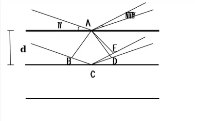
(12) 2.3. X-ray diffraction Considering now the path difference between successive planes when the. incident beam remains fixed at the Bragg angle θ as in Fig. 2-3, but with the diffracted ray leaving at an angle θ+∆θ, corresponding to the intensity I in the spectrum line an angular distance ∆θ away from the peak. The path difference between waves from successive planes is now21). BC + CE = d ⋅ sin θ + d ⋅ sin( θ + ∆θ ) = d ⋅ sin θ + d sin θ cos ∆θ + d cos θ sin ∆θ. (2-3). with BC and CE is the path difference between the successive incident beams, and d is the interplanar distance. If ∆θ is not too large, we can write cos ∆θ ≅ 1 and sin ∆θ ≅ ∆θ, in which case. BC + CE = 2d sin θ + d cosθ ⋅ ∆θ = nλ + d cos θ ⋅ ∆θ. (2-4). which λ is the wavelength of the incident X-ray. Therefore the phase δ per interplanar distance is 2π 2π nλ + d cos θ ⋅ ∆θ λ λ 2π = 2πn + d cos θ ⋅ ∆θ λ. δ =. (2-5). Since a phase difference of 2πn produces the same effect as a zero phase, we can write the effective phase difference as δ =. 2π d cosθ ⋅ ∆ϑ λ. (2-6). We obtained the result that the distribution of intensity I in a spectrum line a distance R from the grating is effectively φ I = ( )2 R. 1 Nδ 2 1 sin 2 δ 2. sin 2. (2-7). the maximum intensity is 12.
(13) φ I max = ( ) 2 N 2 R. (2-8). where φ is the amplitude at unit distance from the grating, N the total number of grating apertures, and δ the phase change per aperture. I I max. =. 1 N2. 1 Nδ 2 1 sin 2 δ 2. sin 2. (2-9). Since (1/2)Nδ will change much faster than (1/2)δ, the function will reach its first minimum before (1/2)δ is very large. If we replace sin(1/2 δ) by (1/2)δ, and will get I I max. =(. sin. 1 Nδ 2 )2. (2-10). 1 Nδ 2. The ratio I/Imax will fall to 1/2 when 1 Nδ 1 2 = 1 2 Nδ 2. sin. (2-11). The solution to the equation yields the required phase change corresponding to the half maximum. It may be obtained 1 2π N d cosθ ∆θ = 1.39 2 λ. (2-12). or, since D= Nd 2 ∆θ =. 0.89λ D cos θ. (2-13). The β s is taken as the width at half maximum from ∆θ to −∆θ, and βs =. 0.89λ D cos θ. ( radians). (2-14). 13.
(14) where λ is the wavelength of the x-ray source, and D is the size of the particles.. ∆θ. θ d. Fig. 2-3. The crystalline planes of the materials. Considering hexagonal unit cell which is characterized by lattice parameters a0 and c0 . The plane spacing equation for the hexagonal structure is. 1 4 h 2 + hk + k 2 l 2 + 2 = d 2 3 a2 c. (2-15). Combining Bragg’s law (λ=2 d sin θ) with (2-15) yields :. 1 4 h 2 + hk + k 2 l 2 4 sin 2 θ + 2 = = d 2 3 a2 λ2 c. (2-16). Rerranging gives. λ2 4 h 2 + hk + k 2 l 2 + 2 } sin θ = { 4 3 a2 c 2. (2-17). Thus the lattice parameters can be estimated from (2-17).. 14.
(15) 2.4. Raman spectroscopy Raman scattering involves a change in photon frequency.. When light. encounters the surface of a semiconductor, most of the light is reflected, transmitted, absorbed, or Rayleigh scattered, because of first-order elastic interactions with electrons, phonons, and impurities. There is no change in photon frequency; but a small part of the light interacts inelastically with phonon modes, producing outgoing photons whose frequencies are shifted from the incoming values. Raman-scattered photons.. These are the. They gain energy by absorbing a phonon (anti-Stokes. shifted), or lose energy by emitting one (Stokes shifted), according to the energy and momentum conservation rules: ws = wi ± Ω q s = qi ± K where wi and ws are the incoming and scattered photon frequencies respectively, qs and qi are the incoming and scattered photon wavevectors respectively, and Ω and K are the phonon frequency and wavevector respectively.. Raman scattering is. inherently a weak process, but lasers provide enough power that the spectra can be routinely measured. The frequency-shifted photons can be described as carrying side-bans at the phonon frequency, which arise from the nonlinear interaction between the radiation and the semiconductor lattice. Cardon (1975a) points out that the classical theory of this nonlinear Raman interaction depends on the polarizability of the lattice, which is the change in its electric susceptibility χ due to excitation of the crystal. This means that the dielectric functionε(w) varies slightly with lattice spacing . If u is a coordinate describing the phonon normal modes, this dependence can be written as a Taylor series expansion:. 15.
(16) 1 d 2ε dε ε (w, u ) = ε (w ) + u + 2 2 du du . 2 u + ... . Since P=εE, this means that the dipole moment induced by the radiation electric field is:. ~ dε ~ 1 d 2ε ~ ~ p = ε ( w)E + uE + 2 u 2 E 2 du du It is the small non- linear terms uE, u2 E, … that generate the weak Raman side-bands. The phonon coordinate for a mode with frequency Ω has the form E=E0 coswt. Then the induced dipole moment contains terms [cosΩt]n coswt, where n=1,2,3,…. From standard trigonometric identities, these terms can be expressed in. an alternate form cos(w ± nΩ)t, n=1,2,3,… ,so that the light re-radiated by the oscillating polarization vector has components at the frequencies w ± nΩ.. The. leading term represents Raman-shifted bands at frequency w+ Ω and w- Ω, the anti-Stokes and Stokes line. The other weaker terms represent the interaction of the phonton i-th multiple phonons (n= 2, 3, … ) All the Raman parameters-band frequencies and intensities, line-shape and line-width, polarization behavior-can be used to characterize the lattice and impurities in a semiconductor. The intensity gives information about crystallinity, since it may be reduced in crystals damaged by ion bombardment or other means.. The. line-widths increase when a material is damaged or disordered, because these conditions increase phonon damping or change the rules for momentum conservation in the Raman process. All these capabilities can be used as a judgment for layered microstructures as well as bulk material, subject only to the limitation that the penetration depth of the exciting radiation ranges from a few hundred nanometers to a micrometer.. 16.
(17) Atomic Force Microscopy22). 2.5. The success of the scanning tunneling microscopy has led to the invention of a host of other “scanning probe” microscopes, which relies on mechanically scanning a sharp tip over a sample surface. The atomic force microscopy is one of the most successful of these new devices. From Figure2-4, description of the principle operation of an STM as well as that of an AFM. The tip follows contour B, in one case to keep the tunneling current constant (STM) and in the other to maintain constant force between tip and sample (AFM, sample, and tip either insulating or conduction). The STM itself may probe forces when a period force on the adatom varies its position in the gap and modulates the ac voltage on the tip, or from an externally applied magnetic field for adatoms with a magnetic moment.. 2.6. Measurement of Thin Film Thickness. 2.6.1. Ellipsometry24,25,26). Also known as polarimetry and polarization spectroscopy, the technique of ellipsometry is a century old and has been used to obtain the thickness and optical constant of films. The method consist of measuring and interpreting the change of polarization state that occurs when a polarized light beam is reflected at non- normal incidence from a film surface.. 2.6.2. Interferometry of Transparent Films27,28). Transparent films are ideally suited for interferometry because interference of light occurs naturally between beams reflected from the two film surface. Since 17.
(18) different interfaces are involved for the beams that interface, precautions must be taken to account for phase changes on reflection.. 18.
(19) Chapter 3. 3.1. Experiment details. Sample preparation. 3.1.1. Target preparation. The target is GaSe crystal, which was grown by Vertical Bridgeman method. Because the ejected plume has large kinetic energy due to its weak bonding force in this orientation during the process of deposition, the (001) orientation of the GaSe crystal was placed normal to the target. In order to maintain flatness and clean of target surface, we lifted off the cleaved surface of crystal before sputtering every time. By this way the plume would not emit in random direction or be quenched due to the pits of the target surface.. 3.1.2. Thin film growth. The thin film of GaSe were prepared by pulsed laser deposition utilizing a KrF excimer laser (Lamda Physics LPX2001 whose data sheet is list in Table 3-1).. Table3-1 LPX210i. Puls. Max.. (KrF). Energy Rep.. Average Puls Duration. Beam. Beam. Power. (nominal). Dimensions. Divergence. 5W. 25ns,FWHM. 5-12 x 23. 1 x 3 mrad. mm2 (VxH). (VxH). Rate. Specifications 700mJ. 100. 19.
(20) High quality c-cut sapphire wafers, Si(111) and GaN(0001) were used as substrates. All the substrates have 10*10mm2 or 20*10mm2 in size and are cleaned before putting on the substrate holder for deposition. We clean our three kinds of substrate in different methods. We describe these clean process as follows. For Si(111) substrates: (1) Rinsed in D.I.water by supersonic oscillator in 5 min. (2) Rinsed in IPA(Isotropic Alcohol) solutions by supersonic oscillator in 5 min. (3) Rinsed in D.I.water by supersonic oscillator in 2 min. (4) Cooked in NH4 OH:H2 O2 :H2O=1:4:20 solutions between 75o C~85o C in 15min. (5) Repeat the step (1). (6) Dried with the N2 gas. For GaN substrates: (1) Rinsed in D.I.water by supersonic oscillator in 5 min. (2) Rinsed in IPA(Isotropic Alcohol) solutions by supersonic oscillator in 3 min. (3) Soaked in HCl:H2 O=1:1 solutions in 3min. (4) Rinsed in D.I.water by supersonic oscillator in 3 min. (5) Soaked in HF:H 2 0=1:15 in 10 sec. (6) Repeat the step (1) (7) Dried with the N2 gas. For Sapphire substrates: (1) Rinsed in D.I.water by supersonic oscillator in 5 min. (2) Rinsed in ACE(Acetone) by supersonic oscillator in 2 min. (3) Rinsed in IPA(Isotropic Alcohol) solutions by supersonic oscillator in 5 min. (4) Repeat the step(2). (5) Repeat the step(1). 20.
(21) (6) Dried with the N2 gas. The growth of thin films was carried out in a high vacuum system with a base pressure below 2x10⁻⁶ mbar (Figure2-1). In our system, we used a focus lens(f=25) to convergent the laser beam through a window onto the target, which makes 45 degree to the normal of the target. The laser energy is 300mJ per pulse. During the deposition of GaSe epitaxy film process, the substrate temperature was set at 425o C. The substrate is heated by a halogen light bulb through the program enable temperature controller. The frequency is 2 pulses per second. In order to confirm that the laser beam vaporized the target uniformly and efficiently, the distance from the target and substrate is adjusted to be 4 cm, which is an empirical value of through failure trials. At the same time, the laser beam was scanning by a lens which was mounted on a step motor. In order to prevent laser beam being focused on the same spot that leads to film quality non-uniform or poly-crystalline.. 3.2. Comparison of films qualiyies on different substrates. 3.2.1. X-ray diffraction. The crystal structure of the as-grown as well as in-situ annealing thin films were inspected by X-ray diffractometer JPN MAC Science MXP18 offered by NTHU using a Cu Kα X-ray source (λ=1.542A). The maximum voltage of the system is 30KV with a maximun current 20mA. The scanning step is 0.02o and scanning speed is 4 degree/min.. 21.
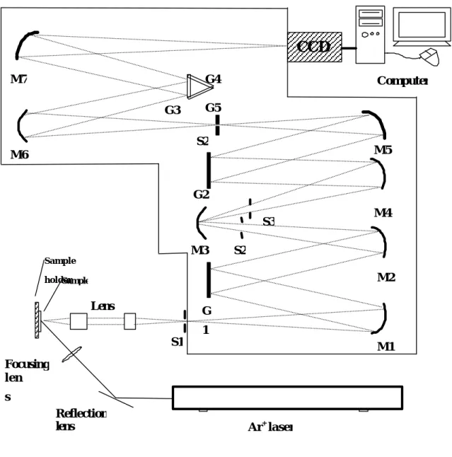
(22) 3.2.2. Atomic Force Microscopy. A Digital AFM is used to analyze the surface of the thin film (Figure3-1). The atomic force microscope is scanned-proximity probe type. The small probe-sample separation (on the order of the instrument ’s resolution) makes it possible to take measurement over small area.. 3.3. Measurements of optical properties Raman detedtion system: The Raman scattering was measured with an Ar- ion. laser(Coherent INNOVA 90) as an excitation source emitting at a wavelength of 488nm. The spectra were measured at room temperature. In Figure3-2, the incident beam was in 45o reflection geometry with the samples mounted on the holder to a spectrometer, which is equipped with a liquid-nitrogen cooled CCD detector array (Phometrics CC200). The laser beam was focused by a converging lens (f=5cm) in beam spot size = 30~50μm (in diameter), an average power about 70mW. The scattered light was collected by a camera lens and image onto the entrance slit of the Spex1877C. As also shown in Figure3-2, the block diagram of our Raman detection system consist of a triplemate (Spex1877C), a liquid-nitrogen cooled charged coupled device (CCD) detector array (Phometric CC200). The scattered light passes through the entrance (S1) to be collimated by a sphere lens M1 ontoG1 and then it is dispersed onto M2. After passing through S2, which determines the bandpass of the filter stage, the light strikes the spatial- filter mirror (M3) and passes through a fixed slit, which eliminates much of stray light. Repeatedly the light is collimated by M4 and dispersed by G2, in an opposing direction to cancel the effects of the initial dispersion, then focused by M5 onto the exit slit of the filter stage (S3) which controls the resolution. 22.
(23) of the spectrograph. In this final stage, the light is again collimated (M6) and dispersed on whichever of the turreted grating (G3, G4, and G5 as grating of 600, 1200, 1800 grooves/mm, respectively) is selected by the user. Which we use here is G4. The camera mirror (M7) projects a flat image onto the focal plane, which can be detected by a CCD. The slit width of S1, S2, S3 used was 0.5, 0.3, 0.1 mm, respectively which led to a resolution of 0.78cm-1 .. 23.
(24) Chapter 4. Results and Discussion. 4.1 Results of X-ray diffraction measurement The optimal growth conditions of as-grown GaSe thin films, which have been determined completely by former researcher in our group, are operated at substrate temperature of 425 0 C, laser deposition rate of 2 Hz, and laser energy density of 1.17 J/cm2 . The best conditions are therefore used to study the behavior of initial growth by changing different deposition times during film growth. Figures 4-1(a), 4-2(a), and 4-3(a) present XRD results of GaSe thin films with different deposition times on the three different substrates. The thickness of these films with different deposition times, 5, 15, 30, 50, and 60 minutes, which were evaluated by Alpha stepper, correspond to the thickness of 10, 30, 56, 95, and 114 nm, respectively (The resolution of Alpha stepper is about 10nm. Thus we measure the sample whose deposition time is longest 4 to 5 times and calculate the average measured thickness values. The samples whose deposition time is shorter were estimated from the deposition rate. It is apparent that the thin film thickness of different deposition time will have an inaccuracy ~10nm). The growth rate could be estimated to be about 1.8 nm/min. Compared with the three different substrates, except the peaks of (002) and (004) planes, the (100) and (101) diffraction peaks only exist in the GaSe/GaN and GaSe/sapphire as the thickness is beyond 30 nm. Furthermore, the length of a-axis (a0 ) was estimated from the (100) diffraction peak position by means of decoupling the (100) and (101) peaks. At the thickness of 10nm and 30nm in GaSe/GaN series, the estimated values of a0 are 3.722 and 3.766 nm, respectively. Besides, the lattice constant a0 of GaSe/Sapphire series is 3.733 and 3.745 nm at those different thicknesses. These values of a0 are almost the 24.
(25) same with the bulk value. As the GaSe film thickness increases the (004) preferred orientation (2θ=22.2610 ) is gradually observable and the diffraction peaks from (100) and (101) planes will be eliminated. The fact is due to the larger lattice mismatch between GaSe thin film and substrate, such as GaN and sapphire, which make atoms mis-aligned during the initial stage of deposition. Oppositely, the silicon substrate with lattice mismatch of 2 % could possess better growth environment for layered GaSe. Besides, when the thickness is increased, FWHM of main peak will get smaller and these fitting results are listed in Table 4-1. The FWHM of diffraction peak corresponding grain size could be described by Scherrer’s formula and listed below: t=. 0 .9 λ B cos θ B. (4-1). where the t is the grain size, λ is the wavelength of incident wave, θB is peak position of (004), and B is broadening of diffraction line measured at half its maximum intensity. Figure4-5(b) shows the grain size of different thickness in the three kind of substrate. According to these analytic results, it is found that the quality of GaSe film with larger thickness will become better even in the GaN and sapphire substrate. Observably, the effects of different lattice mismatch occur below the thickness of 30 nm. Figure4-1(b), 4-2(b), and 4-3(b) show the different deviation of main diffraction peak (004) of GaSe thin film on the Si (111), GaN and Sapphire substrates. The 2θ position of the diffraction peak was fit and shown in Figure 4-4(a). From these results, the 2θ position of the diffraction peak would shift to the value of GaSe bulk (2θ=22.2610 ) with increasing thickness. Clearly, in the different substrates, there are different tendency to arrive the position peak of bulk. But, as the thickness is about 120 nm, the 2θ position of GaSe film on the all substrate will virtually arrive at 22.2610 . It means that the effect of lattice mismatch will be eliminated at the thickness. 25.
(26) above 120 nm. Additionally, the lattice constant of c-axis could be calculated form diffraction peak (004). Due to GaSe belong to hexagonal structure the c-axial length of GsSe could be estimated by plane spacing equation:. 1 4 h 2 + hk + k 2 l 2 + 2 = d 2 3 a2 c. (4-2). And Bragg’s law: λ=2 d sin θ. ( 4-3 ). Combining Bragg’s law(4-3) with (4-2) yields:. 1 4 h 2 + hk + k 2 = d 2 3 a2. l 2 4 sin 2 θ + 2 = λ2 c. (4-4). where ( h k l ) is the Miller index, length of c-axial and a-axial were marked with a and c, λ is the wavelength of x-ray. The calculated results are shown in Figure 4-4(b). It is found that the c-axis would be stretched at the initial stage of growth. It is evident that van der Waals epitaxy does not only allow the growth of epitaxial layers despite large lattice mismatch. Due to the much stronger intralayer vs. interlayer bonding interaction, stress caused from GaSe/substrate lattice mismatch could be released follow the increasing thickness. From the XRD analysis, we can easily observe that the initial growth reveal different behavior due to different lattice mismatch. In the MBE system, the growth behavior of GaSe thin films that grow on different lattice mismatch substrates will be observed and propose the same result. In other words, the growth mode of GaSe thin films is belong to layer by layer according to the measurement of the high resolution TEM, RHEED, soft x-ray photoemission. 23) The growth behavior by MBE system is ascribed to the VdWE type. Due to the much stronger intralayer vs. interlayer bonding interaction, no stress, strain or defect are built up in the growing film. We conclude that GaSe thin film on different lattice mismatch substrates by PLD system is not 26.
(27) belong to layer-by-layer growth mode.. 4.2. Analysis of Raman spectra. 4.2.1. Raman spectra of GaSe films. Figure4-6 shows the Raman scattering of GaSe bulk obtained by Bridgman method which has been successfully fabricated by our groups. Raman spectra of GaSe having been studied in the region 10~330cm-1 is listed in Table4-8 measured in the backscattering geometry from the basal plane of crystal. The 2H(ε)-GaSe crystal belonging to the D1 3h space group has the following normal modes: Γ= A1 ’ + 4A2 ’ + 4E’ + 4E”, where one A2 ’ and one E’ are acoustic modes. The A1’, E’, and E” are Raman active optical phonon modes. A1 ’ modes have the symmetry property of x2 +y2 and z2 ; E’, of xy and x2 -y2 ; and E”, of zx and yz. Because of these symmetry properties, nonpolar A1 ’ and E’ modes may be observed in the backscattering geometry. Among them, however, the E’ (LO) mode should only be observed in the forward scattering geometry because it propagates along the basal plane, and thereby has a vanishing momentum along the c axis. In this chapter, we investigate Raman spectra in the range 100cm-1 ~ 400cm-1 including three specific active mode discussed in next section. And then, we use the software of “peakfit demo ” to fit the two A1’ mode and the E’ (LO) mode. After these work, we can determine the position and FWHM of our original data.. 27.
(28) 4.2.2 Raman active A1’ mode shift and different substrate with varied film thickness dependence of FWHM Figure4-10, 4-11, and 4-12 show thickness dependent Raman shift of GaSe crystalline films on the three series substrate. Firstly, from the vibrational behavior of A1’ (134cm-1 and 307cm-1 ) mode, the atomic displacement vector for interlayer and intralayer is shown in Figure 4-7 and 4-8. Due to the atoms vibrate along the c-axial, the orientation and quality of the thin films could be determined by the A1’ Raman mode shift and its FWHM. Therefore, the line-width of A1’mode is also a characterization of disorder in thin film. In the Raman spectra of GaSe films, the strongest peak of A1 ’ mode, whose Raman line are at ~134 cm-1 , was observed. It reveals that these GaSe films possessed preferred orientation (001) not only on the silicon substrate but also on the GaN and Sapphire substrates. Figure 4-13(b) and 4-14(b) present the fitting results of FWHM of A1’mode at 134 and 308 cm-1 and the software “PeakFit Demo ” was used in this systematic analysis. As the thickness increase, the FWHM will become smaller in the case of all substrates and the qualities of films are getting better gradually. Compare with different substrates, at the same thickness of films, the fitting results indicates that GaSe/Si(111) has less disorder than GaSe/GaN and GaSe/Sapphire due to small lattice mismatch. These results are in substantial agreed with XRD data. Figure 4-13(a) and 4-14(a) show the fitting result of the position of Raman active A1’mode at ~134 and 308 cm-1 , whose vibrated along c-axis. From these results, the position of A1’mode of GaSe films, which were grown on the Si, GaN, and sapphire, approach to the A1’mode of bulk GaSe (~134cm-1 ) as the thickness increase. Moreover, the position of A1’mode of the GaSe/Si(111) series converge to the A1’mode value of bulk faster than GaSe/GaN and GaSe/Sapphire series. At identical thickness, GaSe/Si(111) series is always the closest to the single crystalline value. 28.
(29) Due to the effect of lattice mismatch, only fewer stress exist in the GaSe/Si(111) but larger one are observed in the GaSe/GaN and GaSe/Sapphire. These inclinations of A1’mode of thickness dependence are consistent with XRD results. Additionally, at the initial stage of growth, the vibrational frequency of A1’ modes is lower. As the thickness increase, the frequency of A1’ modes is getting higher gradually. According to the XRD results, the assumption is that the existence of certain force will stretch the c-axis of GaSe thin film at the initial stage of growth. Gauthier et al. proposed the relation between crystallographic parameter c and pressure. Experimentally, the frequency of A1’ modes were shifted to higher value when the c-axis of GaSe crystal was compress at room temperature. In other words, the existence of certain pressure, which compress or stretch the c-axis of GaSe, could result from the shift of frequency of A1’ modes. Therefore, during the initial stage of growth, the lattice mismatch would produce the force to stretch the c-axis of GaSe thin film.. 4.2.3 Different substrate with varied film thickness dependence of E’(LO) mode shift and related stress Figure 4-15(a) presents the fitting results of the position of Raman active E’(LO) mode at ~250.5cm-1 . E’(LO) may be reflected backwards at the interface of GaSe and substrates, and this reflection allows us to observe the E’(LO) mode in the backscattering geometry. Since the vibration mode of E’(LO) is parallel to x-y plane and the vibrational behavior of E’(LO) is shown in Figure 4-9, it should be sensitive to the strain introduced by the stress formed on the film-substrate interface. From these results, the Raman line of E’(LO) mode will approach to the value of GaSe bulk as the thickness increase. This results is consistent with XRD data and fitting result of A1’ mode. As can be seen, the stress exists in thin film due to lattice mismatch 29.
(30) between the GaSe film and substrate could be demonstrated by the deviation of higher frequency of E’(LO) mode. E’(LO) mode shifts to high frequency with increasing stressσfrom the pressure effect on GaSe single crystals reveal that w(σ ) = w(0) +. ∂w σ ∂σ. where w(0)(=250.5cm-1 ) is the E’(LO) mode frequency under the zero pressure. w(σ) is proportional to the pressureσ with. ∂w being estimated to be 2.9805 ∂σ. (cm-1 /GPa). This relation was used to estimate the residual stress in the thin film. These results are also shown in Figure4-15(b). Although the GaSe/GaN and GaSe/Sapphire series have great stress in thickness of 9.5 nm, the residual stress gradually release with the increasing thickness due to the Van der Waals Epitaxy. GaSe/Si(111) has better lattice match, so the stress is minima of these three series in the same thickness. Owing to this property, the residual stress could release quite approach to zero pressure state.. 4.3 Atomic Force Microscopy (AFM) The nucleation and growth of thin films and the properties of the resultant thin films are strongly dependent on the deposition condition such as substrate surface quality. According to the ref.[23] the growth mode of GaSe on GaAs(111) substrate, which were fabricated systematically by MBE, were proposed by Rumaner’s research group. According to the Rumaner’s AFM results, GaSe thin film is growing in a mixed layer by layer and island growth mode. Besides, former researcher in our group achieves using the PLD to fabricate the GaSe on sapphire and growth mode of GaSe/sapphire is in a mixed layer by layer and island growth mode. It was found that the individual islands appear to increase in size and number until eventually they 30.
(31) grow together, during the process of deposition. In generally speaking, the growth mode of GaSe thin films, which deposited by PLD, could be supposed Stransky-Krastanov (SK) mode (i.e. layer plus island) which is shown in Fig. 4-16. Consequently, we consider the growth mode affect the tendency of XRD and Raman spectra data we discuss above. The general pictures of the sequences of the PLD growth can be described as layer plus island growth or the so-called Stransky-Krastanov (SK) steps: (1) Formation of adsorbed monomers; (2) Formation of several complete monolayers; (3) 3D islands grow on top of the first full layers; (4) Nucleations or ions (plasma) or atoms with the high kinetic energy to fill the inter-space between high densities of clusters. (5) Complete monolayers continue forming on the surface of the films. Steps 3, 4, and 5 always simultaneously happened and repeated till the end of the growth. Fig. 4-17 and 4-18 show the AFM images of GaSe thin film on Sapphire, whose deposition times are 2 minutes seconds and 9 minutes, respectively. The AFM observations reveal that the films are composed of many island- like structures (Fig. 4-16). As the deposition continues, the amount of individual islands and the size will be increased. Next, these islands would grow together and form the layered structure, as these islands are getting larger (Fig. 4-18). In order to compare with the effect of different lattice mismatch, the AFM images of the initial growth of GaSe/GaN, and GaSe/sapphire are shown in Fig. 4-19, and Fig. 4-20, respectively. It is apparent to observe the different size of cluster in the different substrate. At the same resolution, the Si(111) series seems more flatness(smaller or more high density cluster). This may be due to the small lattice mismatch between GaSe/Si(111). In the larger lattice 31.
(32) mismatch, such as GaSe/GaN and GaSe/Sapphire, the bigger size of cluster could be obtained easily. Because the stress or strain induced by larger lattice mismatch are more non- uniform than these induced by smaller lattice mismatch. Thus we observe that clusters of GaSe/Si(111) are small than those of GaSe/GaN which can be easily observed from Fig.4-19 and Fig.4-20. Initial stage of fabricating GaSe thin films between these three series is different due to different lattice misma tch. This is the critical step of thin film quality. From the analysis of AFM and XRD, our growth mechanism belongs to conventional epitaxy. Former researches conclude that the GaSe/Sapphire and GaSe/Quartz- glass have the same behavior because the deposition thickness is above 80nm. From the results of XRD and Raman, as the thickness is above 80nm, the quality of GaSe films on small or large lattice mismatch approach closer. After analyzing the thinner GaSe thin film, the different behavior was observed as the thickness below 80nm. When the thickness below 80nm, it is obviously that the thin film quality of different lattice mismatch are different. Hence, the growth mode of critical mechanism is different by MBE system. For this reason, GaSe thin films that deposited by PLD system do not belong to VdWE or qusi-VdWE.. Table4-1: XRD (004) peak FWHM of GaSe thin films on Si(111), GaN and Sapphire substrates with varied thickness.. Substrate thickness(nm) 10 30 56 96 114. Si(111). GaN. 0.27057 0.24777 0.21292 0.19716 0.14462. 0.74365 0.67081 0.25709 0.23683 0.2016. 32. Sapphire 0.83939 0.6847 0.3482 0.29626 0.2708.
(33) Chapter 5. Conclusions. We have successfully fabricated GaSe thin films on Si(111), c-cut GaN, c-cut Sapphire with varied thickness. From XRD analysis, it is obvious that GaSe thin film have (004) plane prefer orientation. Although large lattice mismatch like GaSe/GaN(~15%) and GaSe/Sapphire(~25%) reveal (100) and (101) planes, only (004) and (002) are apparent when the thickness above 56nm. We calculate the c-axis length from the (004) peak position, it is found that the c-axis length become larger than bulk value. At the same thickness, c-axis length of GaSe/Si(111) always closer to bulk value than GaSe/GaN and GaSe/Sapphire. When the thickness is increased, the length of c-axis turns into shorter and closer to bulk value. In addition, the grain size becomes larger when we continue to deposit. And the crystalline become better when thickness of films increase. The crystalline of GaSe thin film can be also evaluated by Raman A1’mode which vibrates along c-axis. The more consistent frequency and linewith of A1’ mode with those of GaSe bulk, the better crystalline GaSe thin film is. We can also see the strongest peak of A1’mode in the Raman spectra. It reveals that the film has high oriented (00l) epitaxially and shift to lower frequency compared with bulk value at initial stage of growth. Due to the vibration of A1 ’mode is parallel to the c-axis, the length of c-axis would be related to Al’mode position. Gauthier et al. proposed the relation between crystallographic parameter c and pressure. The FWHM indicates the tendency is consistent with XRD result. The E’(LO) mode shows the residual stress and the stress will release with the thickness is increased. The result of E’(LO) mode of GaSe thin films on different substrates with varied thickness indicate that this is not like VdWE obviously.. 33.
(34) From AFM, we have confirmed that the growth mode of GaSe is SK. And the clusters size of initial growth are different from substrate. It is speculate that the different cluster size will affect the consequent result we observe in XRD and Raman spectra. The initial growth behavior is distinct from it of MBE. During our research, we use α-stepper to measure the thickness of thin films. Because the resolution of α-stepper is more than 10nm, the thickness of thin film have inaccuracy. When the thickness become thinner (<50nm), the inaccuracy will turn into large. In the future, if the research will be pushed to thinner(<10nm), it is suggested that other tools(Chapter 2.6) could be applied to improve the accuracy of thickness.. 34.
(35) References 1. Ueno K, Okada R, Saiki K, et al., SURF SCI, 514 (1-3) 2002 2. Meng S, Schroeder BR, Bostwick A, et al., PHYS REV B 64 (23) 2001 3. Budiman M, Okamoto T, Yamada A, et al., JPN J APPL PHYS, 37 (10) 1998 4. Allakhverdiev K, Fernelius N, Gashimzade F, et al., J APPL PHYS 93 (6) 2003 5. Shi W, Ding YJJ, Mu XD, et al., APPL PHYS LETT 80 (21) 2002 6. Abidri B, Lacharme JP, Ghamnia M, et al. SURF REV LETT 6 (6) 1999 7. Meng S, Schroeder BR, Olmstead MA, PHYS REV B 61 (11) 2000 8. Jedrecy N, Pinchaux R, Eddrief M, PHYSICA B 248 1998 9. C. Tatsuyama, H. Nishiwki, K. Asai, et al., APP SUR SCI, 117/118 1997 10. Le Thanh Vinh, M. Eddrif, et al., J. APPL. PHYS 81 (11) 1997 11. Ueno, K.; Sakurai, M.; Koma, A., Journal of Crystal Growth Volume: 150, Part 2 1995 12. Izumi T, Nishiwaki H, Tambo T, et al., APPL SURF SCI 104 1996 13. ABE H, UENO K, SAIKI K, et al., JPN J APPL PHYS (10A) L1444-L1447 1993 14. S.H. Li, W.F. Hsieh, C.S. Chang, Fabrication and Characterization of Epitaxial GaSe Thin Film by PLD/A thesis for the degree of master in Electro-Optical Engineering, NCTU June 2001. 15. M.D. Lee, W.F. Hsieh, C.S. Chang, Fabrication and Characterization of layered semiconductor GaSe thin film on chemically prepared Si(111) substrates by PLD/ A thesis for the degree of master in Electro-Optical Engineering, NCTU June 2002. 16. Douglas B. Chrisey, Graham K. Hubler, Pulsed Laser Deposition of Thin Films/A Willy-Interscience Publication.. 35.
(36) 17. Singh, N. B.; Suhre, D. R.; Balakrishna, V.; Marable, M.; Meyer, R.; Fernelius, N.; Hopkins, F. K.; et. al., Progress in Crystal Growth and Characterization of Materials, Volume: 37, Issue: 1, 1998 18. Singh, N.B.; Henningsen, T.; Balakrishna, V.; Suhre, D.R.; Fernelius, N.; Hopkins, F.K.; Zelmon, D.E., Journal of Crystal Growth, Volume: 163, Issue: 4, June, 1996. 19. Singh, N.B.; Narayanan, R.; Zhao, A.X.; Balakrishna, V.; Hopkins, R.H.; Suhre, D.R.; Fernelius, N.C. et. al., Materials Science and Engineering: B, Volume: 49, Issue: 3, October 24, 1997. 20. Kador, L.; Braun, M.; Allakhverdiev, K.R.; Salaev, E. Yu., Optics Communications, Volume: 143, Issue: 1-3, November 1, 1997. 21. N. Aoto, K. Sunouchi, A. koma, Extend abstrates of 15th conf. Of solid state Devices and Materials, Tokyo, 1983. 22. G. Binning, C. F. Quate, Atomic Force Microscope, PHYSICAL REVIEW LETTERS volumn56, number9, 1986. 23. W. Jaegermann, R. Rudolph, A. Klein, C. Pettenkofer, Thin Solid Film, 380(2000) 24. W. A. Pliskin and S. J. Zanin, in Handbook of Thin Films Technology, eds. L. I. Maissel and R. Glang, McGraw-Hill, New York(1970) 25. L. I. Maissel and M. H. Francombe, An Introduction to Thin Films, Gordon and Breach, New York(1973) 26. Azzam L. E. and Bashare N. M., 1977,” Ellipsometry and polarized light”, North-Holland. 27. R. Swanepoel, Determination of the thickness and optical constants of amorphous silicon, J. Phys. E, Vol.16 1983 28. J. C. Manifacier, J Gasiot, et al, A simple method for the determination of the optical constants n, k and the thickness of a weakly absorbing thin film., J. Phys. E, Vol.9 1976. 36.
(37) 29 A. M. kulibekov, H. P. Olijnyk, et al, Phys. Stat. Sol. 235 No.2 2003.. a. 37. b.
(38) c. d. Fig.1-1 Crystallographic structure of GaSe (a) a single layer of GaSe (b) unit cell presented by the broken lines (c) composition of a layer (d) projection of atomic position on a layer plane.. 38.
(39) Figure2-1 Pulsed Laser Deposition system. 39.
(40) Fig.2-4 Atomic Force Microscopy. 40.
(41) Fig.3-1. The AFM feedback loop. 41.
(42) CCD M7. G4 G3. Computer. G5 S2. M5. M6 G2 S3 M3. M4. S2. Sample. M2. holder Sample. Lens. G 1 S1. M1. Focusing len s Reflection lens. Fig. 3-2. Ar+ laser. Raman detection system. 42.
(43) (a). Intensity. Si(111) series ( 0 0 4 ). (002) 114nm 95nm 56nm 30nm 10nm. 10. 15. 20. 25. 35. 40. 2 theta. Intensity. (b). 114nm 95nm 56nm 30nm 10nm 18. 20. 22. 24. 26. 28. 2 theta Fig.4-1: (a) XRD pattern and (b) (004) peak with varied thickness of GaSe thin films on Si(111) substrate. 43.
(44) (a) (004). Intensity. (002) 114nm 95nm 56nm x6. (101). (100). 30nm 10nm. x5 10. 15. 20. 25. 2 theta. 30. 40. Intensity. (b). 114nm 95nm 56nm 30nm 10nm 18. 20. 22. 24. 26. 28. 2 theta Fig.4-2: (a) XRD pattern and (b) (004) peak with varied thickness of GaSe thin films on GaN substrate. 44.
(45) (a) (004). (002). Intensity. 114nm 95nm 56nm. x2 (100). 10. (101). x3. 30nm. x3. 10nm. 15. 20. 25. 2 theta. 30. 35. 40. (b). Intensity. 114nm 95nm 56nm 30nm 10nm. 18. 20. 22. 24. 26. 28. 2 theta Fig.4-3: (a) XRD pattern and (b) (004) peak with varied thickness of GaSe thin films on Sapphire substrate. 45.
(46) (a) 22.30. 2 theta(degree). 22.25. 22.20 Si GaN Sapphire. 22.15. 22.10. 22.05 0. 10. 20. 30. 40. 50. 60. 70. 80. 90. 100. 110 120 130. thickness(nm). (b) 16.12 Si GaN Sapphire. 16.10 16.08. C (A). o. 16.06 16.04 16.02 16.00 15.98 15.96 0 10 20 30 40 50 60 70 80 90 100110120130. thickness (nm) Fig.4-4: (a) XRD (004) peak position and (b) related lattice constant c of GaSe thin films on Si(111), GaN and Sapphire substrates with varied thickness. 46.
(47) (a) 0.9 Si GaN Sapphire. Degree. 0.8 0.7 0.6 0.5 0.4 0.3 0.2 0.1 0. 1 0 2 0 3 0 4 0 50 6 0 7 0 8 0 9 0 1 0 0 110 1 2 0 1 3 0. thickness (nm) (b) 60. grain size (nm). 55. Si GaN Sahhoire. 50 45 40 35 30 25 20 15 10 0. 10 20 30 4 0 5 0 6 0 70 80 90 100 110 120 130. thickness (nm) Fig.4-5: (a) XRD (004) peak FWHM and (b) related grain siez of GaSe thin films on Si(111), GaN and Sapphire substrates with varied thickness. 47.
(48) 2500. 1 3 5 . 1 5 ( A 1 '). intensity(a.u). 2000. 1500. 214.28(E'(TO)). 3 0 7 . 9 8 ( A 1 '). 1000. 500. 0 200. 300. wavenumber(cm. -1. 400. ). Fig.4-6 Raman spectra of GaSe bulk. Fig.4-7: Atomic displacement vector for interlayer and intralayer Raman-active A1’(143cm-1 ) optical mode. 48.
(49) Fig.4-8: Atomic displacement vector for interlayer and intralayer Raman-active A1’(307cm-1 ) optical mode. Fig.4-9: Atomic displacement vector for interlayer and intralayer Raman-active E’(LO)(250.5cm-1 ) optical mode. 49.
(50) A1'mode. E'(LO)mode A1'mode 114nm. Intensity. 95nm 56nm. 100. 150. X3. 30nm. X5. 10nm. 200 250 300 wavenumber(cm-1). 350. 400. Fig.4-10: Raman spectra of GaSe films deposited on Si(111) substrate.. E'(LO)mode A1'mode. A1'mode. 114nm. Intensity. 95nm 56nm. 30nm 10nm. 100. 150. 200 250 300 waveunmber(cm-1). 350. 400. Fig.4-11: Raman spectra of GaSe films deposited on GaN substrate.. 50.
(51) E'(LO)mode A1'mode. Intensity. A1'mode. 114nm 95nm 56nm 30nm 10nm. 100. 150. 200 250 300 wavenumber(cm-1). 350. 400. Fig.4-12: Raman spectra of GaSe films deposited on Sapphire substrate.. 51.
(52) (a). A1'mode(134cm-1). 134 133 132 131 130 129. Si GaN Sapphire. 128 127. 0 10 20 30 40 50 60 70 80 90 100110 120 130. thickness(nm). FWHM of A1'mode(134cm-1). (b) 15 Si GaN Sapphire. 14 13 12 11 10 9 8 0. 10 20 30 40 50 60 7 0 80 90 1 0 0 110 120 130. thickness (nm) Fig.4-13: (a) Position and (b) FWHM of A1’mode(134cm-1 ) peak of GaSe thin films deposited on Si(111), GaN and Sapphire substrates with varied thickness. 52.
(53) (a). A1'(308.1)cm. -1. 308 307 306 305 304 Si GaN Sapphire. 303 302 301 300 0. 10 20 30 40 50 60 70 80 90 100 110 120 130. thickness (nm). FWHM of A1'mode(308.1cm-1). (b) 14. Si GaN Sapphire. 13 12 11 10 9 8. 0 10 20 30 40 50 60 70 80 90 100110 120130. thickness (nm) Fig.4-14: (a) Position and (b) FWHM of A1’mode(308.1cm-1 ) peak of GaSe thin films deposited on Si(111), GaN and Sapphire substrates with varied thickness.. 53.
(54) E'(LO)mode (250.5cm-1). (a). 255. Si GaN Sapphire. 254 253 252 251 250 0. 10 20 30 40 50 60 70 80 90 100 110 120 130. thickness (nm). Stress(GPa). (b). 1.5 1.4 1.3 1.2 1.1 1.0 0.9 0.8 0.7 0.6 0.5 0.4 0.3 0.2 0.1 0.0. Si GaN Sapphire. 0. 10 20 30 40 50 60 70 80 90 100 110 120 130. thickness (nm). Fig.4-15: (a) E’(LO) mode and related (b) stress of GaSe thin film deposited Si(111), GaN and Sapphire with varied thickness. 54.
(55) Figure4-16: Schematic diagram of S.K. groeth mode. Figure4-17: GaSe/Sapphire, Deposition time = 2mins. 55.
(56) Figure4-18: GaSe/Sapphire, Deposition time = 9mins. Figure4-19: GaSe/Si(111), Deposition time = 5 mins 56.
(57) Figure4-20: GaSe/GaN, Deposition time = 5 mins. 57.
(58)
數據
相關文件
You are given the wavelength and total energy of a light pulse and asked to find the number of photons it
Reading Task 6: Genre Structure and Language Features. • Now let’s look at how language features (e.g. sentence patterns) are connected to the structure
refined generic skills, values education, information literacy, Language across the Curriculum (
Wang, Solving pseudomonotone variational inequalities and pseudocon- vex optimization problems using the projection neural network, IEEE Transactions on Neural Networks 17
Define instead the imaginary.. potential, magnetic field, lattice…) Dirac-BdG Hamiltonian:. with small, and matrix
(2) knowing the amount of food, (3) practice of staying awake in the beginning and end of the night, (4) conduct with awareness are also related with Buddhist
Microphone and 600 ohm line conduits shall be mechanically and electrically connected to receptacle boxes and electrically grounded to the audio system ground point.. Lines in
When ready to eat a bite of your bread, place the spoon on the When ready to eat a bite of your bread, place the spoon on the under plate, then use the same hand to take the
