國立交通大學
光電工研究所
博士論文
光電式次兆赫波發射器及其應用
之研究
A Study of Sub-THz Impulse Radio
Photonic Devices and Application
研 究 生:黎宇泰
指導教授:潘犀靈 教授
趙如蘋 教授
光電式次兆赫波發射器及其應用之研究
A Study of Sub-THz Impulse Radio Photonic
Devices and Application
研 究 生:黎宇泰 Student : Yu-Tai Li
指導教授:潘犀靈 博士 Advisor: Prof. Ci-Ling Pan
趙如蘋 博士 Prof. Ru-Pin Chao Pan
國 立 交 通 大 學
光電工程研究所
博 士 論 文
A Thesis
Submitted to Department of Photonics
National Chiao Tung University
in Partial Fulfillment of the Requirements
for the Degree of
Doctor
in
Electro-Optical Engineering
July 2009
Hsinchu, Taiwan, Republic of China
i
光電式次兆赫波發射器及其應用之研究
研究生: 黎宇泰 指導教授: 潘犀靈 教授
趙如蘋 教授
國立交通大學光電工程研究所
摘要
在本論文中,我們研究可利用短脈衝雷射激發之次兆赫波(0.1~1THz)發射器, 包括結合高速光電二極體和印刷天線之次兆赫波發射器以及光導天線兩種型式。 不同型式的元件可產生不同波段之脈衝訊號,我們探討此頻段相關量測系統,元 件特性,以及探討其在寬頻傳輸之應用。 首先我們以波長為 800nm 短脈衝鈦藍寶石雷射激發,以產生出高功率次兆 赫波輻射,並予以調制;本研究中首先探討分別由改良利用低溫成長砷化鎵 (LTG-GaAs) 為基材的分離式傳輸複合光二極體 (STR-PD)以及以砷化鎵/砷化鋁 鎵(GaAs/AlGaAs)為基材的單載子傳輸光二極體(UTC-PD),並結合溝槽天線以及 單極圓碟微波天線之次兆赫波激發器之輻射效率以及其操作行為,以符合寬頻通 訊實驗所需。研究中成功分別驗證了: (1)中心頻率 100GHz(約 75GHz~120GHz) 以及(2)中心頻率 500GHz 的高功率輻射元件之可行性。我們並詳細的探討此兩種 不同的高速二極體結合相同結構之寬頻天線對於兆赫波發射之效果,研究顯示此 兩種設計存在截然不同電流響應機制,但皆具有高功率之輻射輸出功率。 此外,短脈衝雷射亦可激發光導天線以產生兆赫輻射。我們嘗試利用製作程 序較為簡單之多重氧離子佈值之砷化鎵(GaAs:O) 光導天線取代傳統低溫砷化鎵ii
(LT-GaAs)做為激發器,並探討其性質差異。我們量測多重氧離子佈植砷化鎵 (2.5 10× 13ions/cm2
(500keV & 800 keV ),4 10× 13
ions/cm2 (1200keV ) 薄膜材料和 低溫成長之砷化鎵製程之光導天線,驗證其材料替代之可行性。本研究除探討此 兩種光導天線在高偏壓下操作之飽和現象外,亦驗證其產生連續兆赫波之可行 性。 對於兆赫波與次兆赫波之量測,除了可利用 800nm 之鈦藍寶石鎖模脈衝雷 射以及1550nm 光纖雷射做為激發源外,本研究中也架設了利用 800nm 雷射二極 體拍頻連續波激發系統,可做為連續波兆赫波激發之用。在量測此高頻微波的功 率方面,除了分別利用熱輻射儀量測並比較各元件之絕對功率外,也架設基於低 溫砷化鎵光導天線之時域光譜儀,以量測元件輻射出來之電場以及傅式轉換後之 頻譜。為了進一步展示次兆赫波寬頻通訊系統,也架設了一利用高速號角天線(W 頻段,75~110 GHz)做為接受器之寬頻通訊系統,以提高系統之資料傳輸率。 最後在次兆赫波發射器在寬頻通訊應用部分,我們分別做了以下展示: (1) 以Manchester 編碼用改善通訊系統之傳輸品質以及(2)以光纖鎖模脈衝雷射(波長 為1550nm)為系統光源以產生寬頻載波(W 頻段,75~110GHz),並量測此系統之最 高資料傳輸率。在第一部份我們在利用鈦藍寶石鎖模雷射做為激發光源,並以低 溫砷化鎵光導天線做為系統之傳輸接收器,成功的將誤碼率由10-8降低到10-12。 在第二部分,我們利用了光纖鎖模雷射之高脈衝重覆率的優點,成功的展示了在 W 頻段下 2.5Gbit/s 的高資料傳輸率。
iii
A Study of Sub-THz Impulse Radio Photonic
Devices and Application
Student: Yu-Tai Li Advisor: Prof. Ci-Ling Pan
Prof. Ru-Pin Chao Pan
Institute of Electro-Optical Engineering
College of Electrical Engineering and Computer Science
National Chiao Tung University
ABSTRACT
This study investigates of the key components of optical electrical devices operating in the THz and Sub-THz range (0.1~1THz), including photoconductive (PC) antennas and photonic transmitters (PTs). PTs are integrated high speed photo diodes with printed planar antennas designed based on the required radiation frequency range. This study also examines related high frequency measurement systems and broadband communication applications.
The feasibility of several novel photonic transmitters is demonstrated first, which are designed for high peak power generation and wireless ultra-wideband (UWB) communication. Initially, the feasibility of a PT composed of a low-temperature-grown GaAs (LTG-GaAs) based separated-transport-recombination photodiode (STR-PD)
iv
and a micromachined slots antenna is demonstrated. Under femto-second (fs) optical pulse illumination, this device radiates strong electrical pulses (300 mW peak power) at a designed frequency of 500GHz. A traditional LTG-GaAs based PT under high, externally applied electrical fields (>50kV/cm) is then eliminated using our STR-PD based PTs (STR-PTs). Monolithic integration of a GaAs/AlGaAs based uni-traveling-carrier photodiode (UTC-PD) with a broadband micromachined antenna creates UTC-PD based PTs (UTC-PTs) that can also radiate strong sub-THz pulses (20mW peak-power) with a narrow pulse-width (<2ps) and wide bandwidth (100~250GHz). The bias dependent peak output-power of both PTs (UTC- and STR-PD based) makes them highly promising for use as a data modulator/emitter for a photonic UWB system.
This study also describes in detail the characterization of two high power PTs based on two high power photodiodes, UTC-PD and STR-PD. Both PDs have the same depletion layer thickness, i.e. the same theoretical RC-limited bandwidth, and are monolithically integrated with the same broadband micro-machined circular disk monopole antennas. However, the STR-PD based transmitter exhibits a significantly different dynamic and static performance from that of the UTC-PD based transmitter due to a low temperature grown GaAs (LTG-GaAs) based recombination center inside the active region, as well as a much thinner thickness of an effective depletion layer. Under optical pulse excitation (~480pJ/pulse), the STR-PD based transmitter exhibits a markedly lower maximum average output photocurrent (1.2mA vs. 0.3mA) than that of the UTC-PD transmitter. This is despite the fact that the radiated electrical pulse width and maximum peak power, which are determined by the same THz time domain spectroscopic (TDS) system, of both devices are comparable.
v
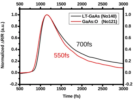
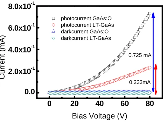
the emission properties of LT-GaAs PC antennas with GaAs:O PC antennas in the pulse and CW mode. GaAs:O PC antennas can generate a higher THz power than LT-GaAs based both in the pulsed and CW modes. The bandwidths of GaAs:O PC antennas and LT-GaAs PC antennas are measured at approximately 1THz both under pulse (TDS) and CW (photomixing) pumping. However, the THz power of LT-GaAs PC antenna becomes saturated in CW mode, while GaAs:O does not. This finding suggests that GaAs:O PC antenna is a more reliable THz emitter than LT-GaAs, which is difficult to reproduce.
To excite THz and Sub-THz radiation, not only are a Ti:Sappire laser (λ=800nm) and fiber mode locked laser (λ=1550nm) used, but a CW excitation system is also established, which consists of two laser diodes (λ=800nm) . The radiated powers of all devices are compared using a Helium-cooled bolometer. Additionally, radiated electrical fields are measured by a TDS system, which is based on LTG-PC antennas. The power spectrum of devices can be determined following fast Fourier transformation (FFT). A wideband communication system is also adopted by using a high speed horn (W band, 75~110GHz) antenna as a receiver to demonstrate the effectiveness of sub-THz wideband communication, which displays an improved data transmission rate.
Finally, this study demonstrates the feasibility of wideband communication applications by using our sub-THz emitters as follows: (1) Communication quality of the LTG-GaAs PC antennas based TDS system is improved by using Manchester coding; and (2) A wideband carrier (W band, 75~110GHz) is generated by using a fiber mode-locked laser as system optical source and determining its maximum data transmission rate. In (1), the Ti: Sapphire laser is adopted as the excitation source and we demonstrate that the bit error rate (BER) improved from 10-8 to10-12 by using
vi
Manchester coding. In (2), data transmission of 2.5Gbit/s at W band is successfully demonstrated by utilizing the advantage of a high repetition rate of fiber mode-locked laser.
vii
Acknowledgements
The author would like to express his gratitude to Professor Ci-Ling Pan and Professor Ru-Pin Pan for providing the opportunity to conduct this research and their advice and supervision during research period.
I am also grateful for the assistance of Professor Jin-Wei Shi and Professor Chi-Wai Chow, especially for their contribution to patiently guide me on my research.
Thanks are also given to group members of the Laser and Electro-Optic (LEO) Laboratory and Liquid Physics Laboratory. I need to appreciate many friends in both groups for their support and company. Without you, it must be very hard to finish many experiments smoothly.
I would also like to thank many friends and cooperation partners whether in the assistance about my life or research. It is really glad and helpful for me to meet you during these years.
Special thanks to my parents, dear members of my family, and my girl friend. Because of your consideration and encouragement, I could concentrate on my research work.
Finally, the thesis is dedicated to all the people who care for me. Thanks all of you, sincerely.
viii
Contents
光電式次兆赫波發射器及其應用之研究... i
A Study of Sub-THz Impulse Radio Photonic Devices and Application ... iii
Acknowledgements ... vii
Contents ... viii
List of Figures ... xi
List of Tables Pages ... xvii
Chapter 1 Introduction ... 1
1-1 THz Gap ... 1
1-2 THz Impulse Radio Communication ... 4
1-3 Generation of Sub-THz Pulses ... 10
1-4 Photodiode Based Photonic Transmitters ... 13
1-5 Low Temperature Grown Based GaAs (LTG-GaAs) or Ion-implanted Materials Based PC Antennas ... 15
1-6 Organization of Dissertation ... 16
Reference ... 19
Chapter 2 THz Photonic Transmitters ... 24
2-1 Introduction ... 24
2-2 Basic Theory ... 27
2-3 Separated-Transport-Recombination Photodiode (STR-PD) ... 31
2-4 Uni-Traveling-Carrier Photodiode (UTC-PD) ... 37
2-5 STR-PD Integrated with Slot Antennas ... 41
ix
Reference ... 48
Chapter 3 Photoconductive Antennas ... 53
3-1 Introduction ... 53
3-2 Basic Theory ... 56
3-3 Material of Photoconductive Antenna ... 61
3-4 Antenna Types ... 63
3-5 Properties of Photoconductive Antennas ... 64
Reference ... 69
Chapter 4 Experimental Methods for Characterization of THz Waves ... 74
4-1 Introduction ... 74
4-2 Power Measurement ... 75
4-2-1 Bolometer ... 75
4-3 Waveform of Spectrum Measurement ... 78
4-3-1 Martin-Puplett Polarization Interferometer ... 78
4-3-2 THz Time Domain Spectrometer ... 82
Reference ... 84
Chapter 5 Performances of THz and Sub-THz Emitters ... 85
5-1 LTG-GaAs & GaAs :O PC Antennas under Pulse Excitation ... 85
5-2 LTGaAs & GaAs :O PC Antennas under CW Excitation ... 91
5-3 STR-PD Combined with Slot Antennas ... 97
5-4 Comparison of UTC-PT and STR-PT ... 101
Reference ... 112
Chapter 6 Sub-THz Impulse Radio Communication ... 115
6-1 Introduction ... 115
x
6-3 Manchester Coding to Improve Link Reliability ... 120
6-4 Impulse Radio Communication under 1550nm Wavelength ... 123
Reference ... 129
Chapter 7 Conclusion and Future Work ... 131
7-1 Conclusion ... 131
7-2 Future Work ... 133
Appendix A ... 135
Publication list ... 137
xi
List of Figures
Chapter 1
Figure 1- 1 Electromagnetic wave spectrum ... 1
Figure 1- 2 Some examples of THz application ... 2
Figure 1- 3 Terahertz gap with respect to source technology. ... 3
Figure 1- 4 The regulated spectrum as designated by the U.S. Federal Communications Commission ... 5
Figure 1- 5 Progress of transmission bits rate for different communication technology ... 6
Figure 1- 6 Diagram of radio-over-fiber communication system ... 7
Figure 1- 7 A vision proposed from NTT to transmitted data >10Gbit/s wireless .... 8
Figure 1- 8 Transmission spectrums ... 9
Figure 1- 9 Attenuation spectrums in rainy day ... 10
Figure 1- 10 Commercial Ti: Sapphire mode locked laser ... 12
Figure 1- 11 Commercial compact Ti: Sapphire mode locked laser ... 12
Figure 1- 12 Schematic of optical heterodyne signal generation in an photonic local oscillator (PLO). ... 13
Figure 1- 13 Schematic of a photonic transmitter consisting of a TWPD monolithically integrated with a planar full-wave single slot antenna 14 Chapter 2 Figure 2- 1 (a) Vertically incident PD and (b) edge coupled incident PD ... 28
xii
Figure 2- 3 An effective diagram of the device ... 30 Figure 2- 4(a)Equivalent circuit of photo diode and (b) simplified equivalent
circuit of photo diode. ... 31 Figure 2- 5 A schematic drawing of energy band and electric field distributed for
traditional GaAs PD under high power excitation ... 32 Figure 2- 6 Traditional LTG-GaAs PD energy band diagram and electrical field
distribution. ... 34 Figure 2- 7 A scheme of change for trap energy band ... 34 Figure 2- 8 Schematic diagram of energy band and electrical field for STR-PD. ... 35 Figure 2- 9 A schematic diagram of electrical field distribution for STR-PD while
applied higher external field. ... 36 Figure 2- 10 Schematic epi-layer structure of GaAs/AlGaAs based UTC-PD ... 38 Figure 2- 11 A schematic diagram of UTC-PD while electrical holes relaxed by
anode ... 38 Figure 2- 12 A schematic band diagram of UTC-PD while incident light of
wavelength 800nm ... 39 Figure 2- 13 A schematic diagram of UTC-PD design ... 39 Figure 2- 14 Top-view of fabricated photonic-transmitter. ... 43 Figure 2- 15 Top-view and cross-sectional view of the demonstrated sub-THz PT.45 Figure 2- 16 Conceptual band diagrams of the demonstrated ... 45
Chapter 3
Figure 3- 1 A schematic diagram for pulsed THz generation by PC antenna ... 57 Figure 3- 2 The simulated curves of two wave with slightly different frequencies.
xiii
Figure 3- 3 Schematic diagram of the PC antenna ... 64
Figure 3- 4 The measurement of carrier life time with both materials ... 65
Figure 3- 5 I-V Curve of GaAs:O and LTG-GaAs ... 66
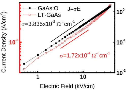
Figure 3- 6 Current density v.s. Electrical field of LTG-GaAs and GaAs:O ... 66
Figure 3- 7 I-V curve of GaAs:O antennas and LT-GaAs antennas under pulse excitation ... 67
Figure 3- 8 I-V curve of GaAs:O antennas and LT-GaAs antenna under CW laser pumping ... 68
Chapter 4 Figure 4- 1 Schematic diagram of a bolometer and its structure drawing ... 76
Figure 4- 2 Schematic of experiment setup for measure the electric characteristics of PC antenna. ... 78
Figure 4- 3 Schematic of a Martin-Puplett-type Fourier Transform Infrared Spectrometer (FTIR) system ... 80
Figure 4- 4 The reflectivity of the electric field dependent with frequency under (a) parallel and (b) perpendicular component. ... 81
Figure 4- 5 Terahertz Time-Domain Spectroscopy ... 82
Figure 4- 6 A picture of measured photonic transmitter in a TDS system ... 83
Chapter 5 Figure 5- 1(a) Photocurrent-bias (b)THz power-bias curve of GaAs:O and LT-GaAs antenna with the same antenna structure ... 86
Figure 5- 2 THz time domain waveform of (a) GaAs:O and (b) LT-GaAs at constant pump power 30mW ... 87
xiv
Figure 5- 3 THz spectrum of (a) GaAs:O and (b) LT-GaAs at constant pump power 30mW ... 88 Figure 5- 4 (a) Time domain waveform (b) Spectrum for both materials ... 89 Figure 5- 5 (a) The amplitude-pump power curve at bias voltage 80V (b) The THz
power-electric field curve at 30mW. ... 90 Figure 5- 6 (a) Photocurrent-bias voltage curve and (b) THz power-bias voltage
curve of GaAs:O and LT-GaAs fabricated with the same dipole antenna ... 91 Figure 5- 7 (a) Photocurrent-bias voltage curve of both materials and (b)
photocurrent ratio of GaAs:O divide to LT-GaAs ... 92 Figure 5- 8 (a) Different dosage density of GaAs:N and LT-GaAs (b) Different
dosage density of GaAs:N and LT-GaAs[48] ... 93 Figure 5- 9 photocurrent-electric field curve and THz power-DC photocurrent
curve for GaAs:O and LT-GaAs DC ... 93 Figure 5- 10 CW THz power-optical pump power for both materials. ... 94 Figure 5- 11 (a) Photocurrent-electric field curve and (b) THz power-electric field
curve. ... 95 Figure 5- 12 THz spectrum of both materials measured by CW heterodyne system
... 96 Figure 5- 13 The Fourier-transformed spectra of our photonic-transmitters with
different active lengths, 23μm (a) and 60μm (b). ... 98 Figure 5- 14 The measured sub-THz intensity vs. optical pumping power under
different reverse bias voltages ... 99 Figure 5- 15 The measured sub-THz intensity vs. reverse bias voltages under
xv
23μm active length. ... 100 Figure 5- 16 The bias dependent measured sub-THz power of (a) UTC-PT, (b)
STR-PT, and (c) LTG-GaAs based PC under different optical pulse energy excitation. (d) shows the top-view of PC dipole antenna ... 102 Figure 5- 17 The power dependent measured sub-THz power of (a) UTC-PT and
(b) STR-PT under different reverse bias voltage. ... 104 Figure 5- 18 Bias-dependent sub-THz power of (a) UTC-PT and (b) STR-PT with
a longer active length of 60μm under different injected optical pulse energy ... 106 Figure 5- 19 The radiated waveform of sub-THz pulses for UTC-PT (a) and
STR-PT (b). ... 107 Figure 5- 20 The normalized power spectrum of (a) UTC-PT, STR-PT and (b)
LTG-GaAs based PC antenna. The inset shows the measured waveform of PC antenna ... 108 Figure 5- 21 Bias dependent waveforms of the radiated sub-THz pulses for (a)
UTC-PT and (b) the normalized and enlarged main peak. The inset shows the normalized peak values versus reverse bias. ... 110 Figure 5- 22 Bias dependent waveforms of the radiated sub-THz pulses for (a)
STR-PT (b) and the normalized and enlarged main peak. The inset shows the normalized peak values versus reverse bias. ... 110
Chapter 6
Figure 6- 1 Schematic diagram of spiral antenna on LTG-GaAs PC antenna based TDS system for Sub-THz communication link ... 118 Figure 6- 2 Frequency response of spiral antenna based communication link
xvi
system ... 118
Figure 6- 3 The input image signal from CCD and received signal after current amplifier ... 119
Figure 6- 4 Schematic diagram of sub-THz communication link system by using Photonic transmitter and W-band power detector ... 119
Figure 6- 5 Frequency response of communication link based on photonic transmitter and W-band power detector ... 120
Figure 6- 6 The schematic experiment setup of TDS based transmission system . 121 Figure 6- 7 Signal coding : (a) OOK coding (b) Manchester coding, and (c) differentially detected Manchester coding ... 122
Figure 6- 8 Signal coding : (a) OOK coding (b) Manchester coding, (c) half-bit delayed and (d) differentially detected Manchester coding ... 122
Figure 6- 9 Measured power spectrum and the inset shows the electrical field .... 122
Figure 6- 10 Bit error rate (BER) versus data rate of OOK transmission in our system ... 123
Figure 6- 11 Measured bit error rate (BER) versus different bias voltage applied on emitter by using Manchester and OOK coding respectively. ... 123
Figure 6- 12 Top view of NBUTC-PT. ... 124
Figure 6- 13 A schematic setup of impulse communication link with optical modulation. ... 125
Figure 6- 14 A schematic setup of impulse communication link with bias modulation. ... 125
Figure 6- 15 Picture of receiver end ... 126
Figure 6- 16 Power spectrum measured at different position. ... 127
xvii
List of Tables Pages
Table 1 Specification of the bolometer used in our measurement ... 76
Table 2 The list of measurement results of UTC-PT and STR-PT ... 109
Table 3 Detail epitaxial structure of UTC-PD ... 135
1
Chapter 1 Introduction
1-1 THz Gap
Terahertz (THz) wave (or Tray) and sub-THz is the electromagnetic wave located between microwaves and infrared light (Fig. 1.1[2]). The THz gap ranges from 0.1 THz to 10 THz, where 1 THz equals 33 wave numbers or 300 μm or 4mev. Lower frequencies, e.g.,) RFs for AM and FM radio as well as microwaves, are based on electric generation controlled by the classical transport of electrons. Radio reception and cellular telephony indoors are allowed for most dielectric materials that are transparent at these frequencies.
Higher frequencies in the spectrum, e.g., IR radiation, visible light and UV, can be generated by quantum transitions. Such frequencies can generate extremely high intensities using lasers and often propagate in a free space based on the laws of geometrical optics. Located between these two regions is the THz regime, which represents the transition between the electric and photonic sources. Thus,
2
electromagnetic radiation in the THz range can be generated both ways. Until recently, the THz region of the electromagnetic spectrum was almost always inaccessible because of inefficient sources and detectors in this gap. This region has attracted considerable attention owing its increasingly diverse array of applications, ranging from communications, security screening to medicine and nondestructive evaluation. [1]
In the 1960s, astrophysics research sparked interest in developing THz detectors because the rotational spectra of some gases of astrophysical and environmental interest fall within this range. In 1975, a pioneering work on picoseconds(ps) photoconductivity in silicon [3,4] led to the development of photoconductive and electro optic methods [5], capable of generating and detecting radiation in the THz frequency range.
An important property of Terahertz is that it does not harm biological cells or the human body towing to its low photon energy. Terahertz is roughly one million
3
times weaker than an X-ray photon, subsequently not incurring damage often associated with ionizing radiation such as X-ray. This property makes the T-ray diagnostic procedure an interesting complement to X-ray radiography. Additionally, each material has its own intrinsic absorption and reflection characteristics in the THz region (referred to as THz finger print), making it useful for identifying their characteristics while it is difficult to distinguish from appearance. Important detective applications are thus possible when combining with another feature of terahertz wave, i.e. it is highly transparent to most non-metallic and non-polar media but highly reflected by metal and absorbed by liquid (like water) or vapor. Such behavior can be exploited to see through packaging and identify metal inside, without damaging the package nondestructive detection. Therefore, terahertz wave has tremendous applications in biomedical science, e.g., skin cancer detection [6], DNA analyzers [7], THz imaging [8], security screening in airports [9], mail inspection [10]) and semiconductor manufacturing [11]. In addition to these applications, several communications applications are available where THz waves will provide new capabilities.
4
(Quantum cascade lasers ( □ ) are progressing downward from higher frequencies, while electronic technology is progressing upward. Frequency multipliers (●) dominate other electronic devices (-) above about 150 GHz. )
Obviously, terahertz technology has many current and future applications, likely playing a larger societal role as other developed bands have such as microwave and infrared bands. This has not yet occurred largely owing to the complexity in achieving a mature technology level in this spectral region. Below 100 GHz, it is common for electronic devices such as amplifiers and oscillators. Above 10 THz, solid-state lasers, light-emitting diodes and optical detectors are also available. Nevertheless, in between, neither of these technologies are particularly practical, resulting in a technology gap in terms of both sources and detectors. Figure 1.3 shows a graph of output power versus frequency for Terahertz gap with respect to source technology. [12] Other CW technologies, including tube devices, e.g., backward wave oscillators, can yield much more power.
1-2 THz Impulse Radio Communication
THz and Sub THz communication
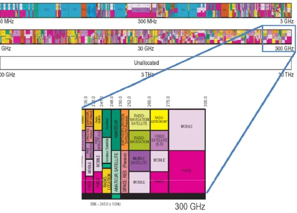
THz and Sub THz communication can refer to either effective data rates up to 100 GHz ~ 1THz bit/s normally on an optical carrier) or communication with a sub-THz or THz carrier wave, which is the focus on this study. Although greater bandwidths can be obtained at optical wavelengths with point-to-point optical communications, communications at THz frequencies are extremely attractive for several reasons. According to the U.S. Frequency Allocation chart in Fig. 2,
5
frequencies (exceeding OR above) 300 GHz are unallocated by the Federal Communications Commission. [1] THz communication is in the infant stage of development, with the first data transmission in this frequency range reported recently. As for the frequency around sub-THz (>100GHz), much space is to be developed. Recently, because some pass bands incur a reasonable loss (e.g., 65~160GHz and 220~300GHz), the millimeter wave (MMW) band above 60GHz (V-band) or 100GHz (W-band) has received increasing attention as a carrier frequency for advanced communication system.
Figure 1- 4 The regulated spectrum as designated by the U.S. Federal Communications Commission
(The regulated spectrum as designated by the U.S. Federal Communications Commission and the THz region, which is completely unallocated at the time of writing. Source:
6
regulated spectrum around 300GHz.)
Wireless communication and Radio-over –fiber
Figure 1.5 illustrates the progress of transmission bits rate for various communication technologies, including wire line and wireless communication. Obviously, wireless communications is advancing to where the focus is shifting from voice to multimedia services. The underlying technology does not appeal to consumers; individuals merely require reliable and cost effective communication systems, capable of supporting all media without time or location constraints. Additionall, an increasing number of new wireless subscribers demand more capacity despite the fact that the radio spectrum is limited. Wideband radio links increasingly communication systems.
Figure 1- 5 Progress of transmission bits rate for different communication technology
The high capacity of optical networks should be integrated with the flexibility of radio networks to satisfy this increasing demand. Such a requirement can be satisfied
7
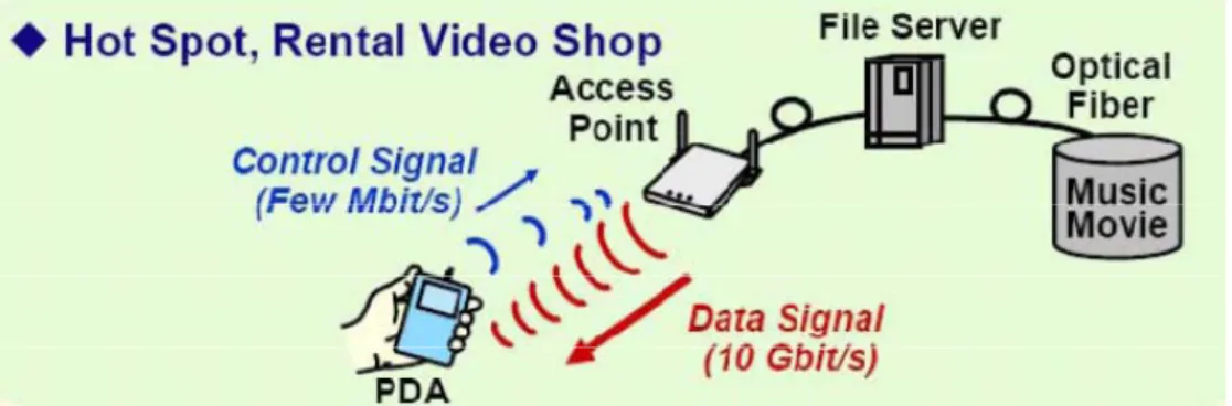
with micro/pico cellular architectures for the above mentioned wideband demands, especially by using fiber based wireless access schemes such as radio-over-fiber (RoF). Such a concept can easily support high speed multimedia, as shown in Fig. 1-6 . RoF communication systems have received considerable interest recently owing to their promising role in satisfying the significantly increasing demand for data capacity [13]. In this system, the high speed data signal is transmitted by an optical fiber for long-haul communication and, then, radiated to a free space for metro environment wireless access by converting the optical signal into an electrical radio signal. A vision from NTT is also proposed in the Fig. 1-7, in which data (including movies or music) can be downloaded from an access point to our portable devices wirelessly and at a high speed rate of up to 10 Gbits/s. Nevertheless, the low frequency band contains too much congestion to develop a >10Gb/s Ethernet, necessitating that the data signal is carried via higher frequency bands.
8
Figure 1- 7 A vision proposed from NTT to transmitted data >10Gbit/s wireless
Impulse radio technology
As mentioned above, the transmission rate in local area networks (LANs) and personal area networks (PANs) must be (increased OR improved) owing to the rapidly increasing data volume handled by (household and office users OR individual users in both household and offices). In wired communications, 10-Gb/s Ethernet (10GbE) has already been standardized and is commercially available (Fig. 1-5). However, (it : what is it?) is only 54 Mb/s for the maximum transmission rate of wireless LANs, i.e. two orders of magnitude slower than that of 10GbE. Consequently, impulse radio (IR) technology has attracted considerable interest owing to its potential to fill this gap [14], [15]. Moreover, IR has other advantages similar to those of ultra wide band communication (UWB) such as secrecy and low power consumption. Therefore, our research of photonic schemes has attempted to derive solutions in order to enhance the transmission performance of IR systems [16], [17]. This is because photonic approaches perform better than electronic ones in terms of generating and detecting short pulse signals at a high repetition frequency in the above fiber-optic transmission systems [18]. Funk et al. demonstrated the feasibility of a photoconductive correlation switch for a receiver in an IR system and reduced interference rejection at a bit rate of 38 Mb/s[17].
9
Disadvantages of communications
Communications at sub-THz frequencies is limited by strong absorption caused by water vapor through the atmosphere, as shown in Figs. 1-8 and 1-9. Another limitation is the low efficiency and relatively low power available from available sources. For a 1-mW source and a detection sensitivity of 1 pW, the working dynamic range is generally 60 dB, allowing communications at a range of 500 m in an atmospheric transmission window with an attenuation of <100 dB/km.[2]
Figure 1- 8 Transmission spectrums
Regardless of the above limitations, this frequency range still has promising communications applications. For instance, atmospheric absorption does not inhibit satellite-to-satellite communications, except for paths grazing the earth atmosphere. Among the advantages of using THz technology is a larger bandwidth, thus yielding a transmission rate higher than that in microwave communications without (switching OR having to switch) to a different set of hardware components such as lasers for optical communications. Indoor wireless communications with THz may
10
also provide multiple data channels with gigabit per second or a larger capacity. The data bandwidth exceeds wireless protocols such as IEEE 802.11b, and the propagation distance, although limited, resembles line-of-sight IR.
Figure 1- 9 Attenuation spectrums in rainy day
1-3 Generation of Sub-THz Pulses
As mentioned in the above section, IR technology can satisfy the demand for low transmit power, high bit rate wireless communications. However, RF impulses generated from pure electronic devices, which normally last one nanosecond or longer, limit the maximum bit rate in wireless communications. Shock wave nonlinear transmission line (belonging to NLTL) [19] can be used to generate THz by using short electrical pulses, which often incur an enormous propagation loss in the free space. The pulse signal can be distributed through a low loss optical fiber. An optical
11
pulse triggered photoconductive (PC) antenna or photonic transmitter (PT) is a promising alternative to radiate the converted electrical signal to the user end. By using photonic technologies such as an optical pulse triggered photoconductive antenna, short pulses lasting only a few picoseconds can be generated and received [20,21]. Based on the maturity of high performing optical pulse sources with wavelengths around 800nm, e.g., solid-state Ti:sapphire mode-locked lasers (Fig. 1-10 and 1-11), low-temperature-grown-GaAs (LTG-GaAs) based photodetectors are regarded as a promising choice for serving as a photonic transmitter to generate continuous wave (CW) THz signal or THz pulses at such an optical wavelength regime [19,22].
A Ti:Sapphire laser provides short pulse (several fs) width and high peak power with repetition rate around 100MHz and can be operated easily under room temperature. Furthermore, other compact commercial products with a higher repetition rate have been proposed (Fig. 1-11), which has the potential for use in constructing a compact system with a higher data rate transmission. Communication links on the sub-THz signal are also demonstrated through either a modulating photoconductive antenna or photonic transmitter [23,24].
This study discusses two photonic transmitters, PD based photonic transmitters (PTs) and LTG-GaAs or ion-implanted materials based photoconductive (PC) antennas. Both devices can generate a short transient current and then radiate sub-THz from integrated antennas while the transient current oscillates in the antennas. PD based PTs are integrated into the design of printed planar antenna with high speed photo diodes, as introduced in the next section. The next section also introduces several promising PDs with a high speed and high output power combined with different designs of antennas. As for the photoconductive antenna, an appropriate
12
material for photoconductive antennas is discussed. Moreover, the emission properties of LT-GaAs PC antennas are compared with those of GaAs:O substrate to study high power THz generation by using PC antennas.
Figure 1- 10 Commercial Ti: Sapphire mode locked laser
13
1-4 Photodiode Based Photonic Transmitters
To alleviate the limitations of all-electronic local oscillators (LOs), a photonic LO (PLO) capable of operating up to (sub-) THz frequencies has received increasing interest. [25] Generally, in a PLO, a (sub-) THz signal is generated by square-law detection of a highly stable phase-locked optical heterodyne signal that uses an ultrafast photodiode (PD). Given its dependence on the beat-frequency difference between the two optical carriers of the heterodyne signal, the frequency of the generated (sub) THz signal can be easily tuned over an ultra wide range by varying the frequency of an optical carrier. In this study, a mode locked pulse laser, which could be viewed as a combination of many frequencies, is used to excite our PLO. A PLO consists mainly of a highly stable optical source and a high-speed PD in the remote photonic (sub) THz transmitter (Fig. 1-12). [25] Figure 1-13 also shows an example of a photonic transmitter consisting of a TWPD monolithically integrated with a planar full-wave single slot antenna. Nevertheless, in contrast with typical GaAs based p-i-n photodiodes (PDs), the decreasing trend of external efficiency for the LTG-GaAs-based PDs is inevitable owing to the existence of recombination centers in the photo-absorption layer [26].
Figure 1- 12 Schematic of optical heterodyne signal generation in an photonic local oscillator (PLO).
14
Figure 1- 13 Schematic of a photonic transmitter consisting of a TWPD monolithically integrated with a planar full-wave single slot antenna
Another attractive alternative for photonic transmitter applications is InGaAs-InP based UTC-PD structures [27]. However, in the case of InP based UTC-PDs under 0.8 μm wavelength excitation, the incident photons produce sufficient photon energy to induce absorption in the entire epi-layer structure. Therefore, our previous study developed a high-speed GaAs/AlGaAs based UTC-PD [28], which consists of a GaAs based p-type photo-absorption layer and an Al0.15Ga0.85As based collector layer to avert undesired photo-absorption that occurs in the collector layer under 800nm wavelength excitation. This study analyzes the power and bias dependent behaviors of a novel sub-THz photonic-transmitter (PT), which is composed of our edge-coupled GaAs/AlGaAs based UTC-PD [28] and a micromachined frequency-independent circular disk monopole antenna [29], capable of eliminating the additional integration of silicon lens with a photonic transmitter [26].
15
1-5 Low Temperature Grown Based GaAs
(LTG-GaAs) or Ion-implanted Materials Based PC
Antennas
Compared with above photonic transmitters, PC antennas provide another alternative means of generating radiation with a higher frequency (up to 1~2THz). The radiation frequency bandwidth depends mainly on PC material properties. The fact that PC devices can generate both broadband THz wave (photocarrier acceleration) and a narrow band THz wave (photomixing) explains why the photoconductive method has become a conventional approach for THz wave generation used in laboratories. The photoconductive approach uses high-speed photoconductors as transient current sources for radiating antennas. Notable examples include LTG GaAs [30], ErAs:GaAs [31] for 800nm light, and LTG InGaAs, InGaAs:Br+ [32] for 1550nm light.
Among the many (attractive OR important) properties of LTG-GaAs include a high dark resistivity (>106 Ωcm [33]), short carrier lifetime(0.25 ps[31, 35]), high carrier mobility (200 μm/V•s [36]), and high breakdown voltage(>5×10⁵ V/cm[37]). Consequently, LTG GaAs is the commonly used material for 800nm pumping PC devices. Nevertheless, these excellent characteristics are difficult to (replicate OR reproduce). Such difficulty is owing to that the quality of LTG GaAs depends not only on the preparation temperature but also on the post thermal annealing conditions. Consequently, some materials grown by ion implantation method have the potential to be a reliable complement of LTG GaAs because controlling the ion dosage and implant energy precisely can overcome the reproducibility limitation of LTG GaAs.
16
As the energy level formed by oxygen ions in GaAs (approaches OR is close to) the Fermi level, the O+ implanted GaAs become almost electrically neutral, thus producing a relatively higher resistance. This study also attempts to elucidate this oxygen ion implanted GaAs material and its THz wave generation properties under both pulsed and CW modes. Its performance is also compared with that of LTG GaAs materials, such as comparing the performance of THz generation with that of LTG GaAs, the saturation behavior and its materials, the maximum output power of THz wave from GaAs:O based PC devices, as well as the screening behavior under CW background illumination. Other interesting research areas for GaAs:O based PC devices include optimization of the generation performance, system compacting) and unique applications.
1-6 Organization of Dissertation
This dissertation is organized as follows:Chapter 2 introduces high-power and high-speed photodiodes (UTC-PD) and separated-transport-recombination photodiode (STR-PD). By inserting a LTG-GaAs layer that has an extremely long carrier time to serve as a recombination center, STR-PD performs better in terms of speed and power than a control PD that hasa pure intrinsic photo absorption layer. Next, the feasibility of a photonic structure is demonstrated, which consists of STR-PD and a micromachined co-planar-waveguide (CPW) fed slots antenna with resonant frequency 500GHz. Next, two high-power photodiodes (UTC-PD and STR-PD) are integrated with the same planar antenna (circular disk monopole antenna with a center frequency around 150GHz) to serve as photonic transmitters. This chapter describes the design principles and device
17 structure in detail.
Chapter 3 introduces several photoconductive antennas consisting of different materials and printed antennas. The basic theories of THz radiation generated from photoconductive (PC) antenna are introduced first. An attempt is then made to identify the proper material type of printed antennas. Next, except for the conventional material LTG-GaAs, the ion implantation method of oxygen and its parameters selection are introduced. Finally, to optimize the preparation conditions, additional properties of important materials such as the carrier concentration, resistivity, carrier mobility and the carrier lifetime are tested and measured. Exactly how LT-GaAs and GaAs:O emitters affect THz radiation of PC antennas is elucidated by comparing thei electrical characteristics.
Chapter 4 describes the experimental setup and measurement method to identify radiation properties of our emitters in sub-THz and THz. The radiated absolute power is (determined OR measured) using a liquid helium-cooled Si bolometer which has been calibrated carefully using a blackbody source. Chapter 4 also introduces a horn antenna owing to its feasibility for a lower band detection (W band, around 100GHz) and higher modulation speed. As for the electrical field measurements, two systems of FTIR and PC sampling are used. Based on use of fast Fourier transforms, the radiation bandwidth of devices is estimated to identify the reliability of our designed devices.
Chapter 5 summarizes in detail all measurement results for both PCs and photonic transmitters. Our discussion of PCs focuses mainly on comparing the properties of PCs: based LT-GaAs and GaAs:O. Preliminary results indicate that GaAs:O is at least as good as LT-GaAs in (generating OR producing OR making) high power THz emitters under both pulse and CW excitation. However, when LT-GaAs is
18
used as the active layer, STR-PT combined with slot antenna can radiate a high output power at a frequency around 0.5THz. Additionally, a further comparison is made of THz emitters made by two high-power photodiodes (UTC-PD and STR-PD by summarizing the measurement results of both PDs combined with the same antenna type. Moreover, the properties of photonic transmitters are compared with those of PC antennas.
Chapter 6 demonstrates the possibility of wideband communication applications by using our sub-THz emitters. First, we improve communication quality of the LTG-GaAs PC antennas based TDS system by using Manchester coding. Next, a wideband carrier (W band, 75~110GHz) is generated by using a fiber mode-locked laser as system optical source and determining its maximum data transmission rate.
Conclusions are finally drawn in Chapter 7, along with recommendations for future research.
19
Reference
[1] M. Tonouci, “Cutting-edge terahertz technology,” Nat. Photonics, vol 1, pp.97-105, Feb., 2007.
[2] Michael J. Fitch and Robert Osiander, “Terahertz Waves for Communications and Sensing” Johns Hopkins Apl Technical Digest, Vol. 25, 4, 2004.
[3] Auston, D. H., “Picosecond Optoelectronic Switching and Gating in Silicon,” Appl. Phys. Lett. 26, 101–103,1975.
[4] LeFur, P., and Auston, D. H., “A Kilovolt Picosecond Optoelectronic Switch and Pockels Cell,” Appl. Phys. Lett. 28, 21–33, 1976.
[5] Valdmani, J. A., Mourou, G., and Gabel, C. W., “Picosecond Electrooptic Sampling System,” Appl. Phys. Lett. 41, 211–212 , 1982.
[6] E. Pickwell and V. P. Wallace, "Biomedical applications of terahertz technology," Journal of Physics D-Applied Physics, vol. 39, pp. R301-R310, Sep 7 2006. [7] M. Brucherseifer, M. Nagel, P. H. Bolivar, H. Kurz, A. Bosserhoff, and R. Buttner,
"Label-free probing of the binding state of DNA by time-domain terahertz sensing," Appl. Phys. Lett., vol. 77, pp. 4049-4051, Dec 11 2000.
[8] X. C. Zhang, "Terahertz wave imaging: horizons and hurdles," Physics in Medicine and Biology, vol. 47, pp. 3667-3677, Nov 7 2002.
[9] J. W. Shockley; W. T. Read, "Statistics of the Recombinations of Holes and Electrons," Physical Review pp. 835 - 842, 1952.
[10] A. W. M. Lee and Q. Hu, "Real-time, continuous-wave terahertz imaging by use of a microbolometer focal-plane array," Optics Letters, vol. 30, pp. 2563-2565, Oct 1 2005.
20
[11] D. Grischkowsky, S. Keiding, M. Vanexter, and C. Fattinger, "Far-Infrared Time-Domain Spectroscopy with Terahertz Beams of Dielectrics and Semiconductors," Journal of the Optical Society of America B-Optical Physics, vol. 7, pp. 2006-2015, Oct 1990.
[12] Crowe, T. W., Bishop, W. L., Perterfi eld, D. W., Hesler, J. L. & Weikle, R. M. Opening the terahertz window with integrated diode circuits. IEEE J. Solid-State Circuits 40, 2104–2110 (2005).
[13] A. Hirata, T. Kosugi, H. Takahashi, R. Yamaguchi, F. Nakajima, T. Furuta, H. Ito, H. Sugahara, Y. Sato, and T. Nagatsuma, “120-GHz-Band Millimeter-Wave Photonic Wireless Link for 10-Gb/s Data Transmission,” IEEE Trans. Microwave Theory Tech., vol. 54, pp. 1937-1944, May. 2006.
[14]L. Larson, D. Laney, and J. Jamp, “An Overview of Hardware Requirements for UWB Systems: Interference Issues and Transceiver Design Implications,” in Tech. Dig. MILCOM2003, Oct. 2003, pp. 863-867.
[15] S. Iida, K. Tanaka, H. Suzuki, N. Yoshikawa, N. Shoji, B. Griffiths, D.Mellor, F. Hayden, I. Butler, and J. Chatwin,“A 3.1 to 5 GHz CMOS DSSS UWB Transceiver for WPANs,” in Tech. Dig. ISSCC 2005, Feb. 2005, pp. 214- 215. [16] E. E. Funk and C. H. Lee, “ Free-Space Power Combining and Beam Steering of
Ultra-Wideband Radiation Using an Array of Laser-Triggered Antennas,” IEEE Trans. Microwave Theory Tech., vol. 44, pp. 2039-2042, Nov.1996.
[17] E. E. Funk, S. Ramsey, C. H. Lee, and J. Craven, “ A Photoconductive Correlation Receiver for Wireless Digital Communications,” in Tech. Dig.MWP‘98, Oct. 1998, pp. 21-24.
[18] K. Uchiyama and T. Morioka, “All-Optical Signal Processing for 160 Gbit/s/channel OTDM/ WDM Systems,” in Tech. Dig. OFC’01, March 2001,
21 paper ThH2-1.
[19] M. J. W. Rodwell, S. T. Allen, R. Y. Yu, M. G. Case, U. Bhattacharya, M. Reddy, E. Carman, M. Kamegawa, Y. Konishi, J. Pusl, R. Pullela,“Active and nonlinear wave propagation devices in ultrafast electronics and optoelectronics [and prolog]” Proceedings of the IEEE, vol. 82, pp. 1037-1059, Jul., 1994.
[20] S. M. Duffy, S. Verghese, K. A. McIntosh, A. Jackson, A. C. Gossard, and S. Matsuura, “Accurate modeling of dual dipole and slot elements used with photomixers for coherent terahertz output power,” IEEE Trans. Microwave Theory Tech., vol. 49, pp. 1032-1038, June, 2001.
[21] Yu-Tai Li, J.-W. Shi, Ci-Ling Pan, C.-H. Chiu, W.- S. Liu, N.-W. Chen, C.-K. Sun, and J.-I. Chyi, “Sub-THz photonic transmitters based on separated-transport-recombination photodiodes and a micromachined slot antenna,”
[22] H. Ito, T. Furuta, F. Nakajima, K. Yoshino, T. Ishibashi, “Photonic Generation of Continuous THz Wave Using Uni-Traveling-Carrier Photodiode,” J. of Lightwave Technol., vol. 23, pp. 4016-4021, Dec., 2005.
[23] Togo, H., Sah, P.-C.P., Shimizu, N., Nagatsuma, T. “Gigabit impulse radio link using photonic signal-generation techniques,” European Microwave Conference 2005, vol. 1, pp. 4-7, Oct., 2005.
[24] T. -A. Liu, G. -R. Lin, Y.-C. Chang, C.-L. Pan, “Wireless audio and burst communication link with directly modulated THz photoconductive antenna,” [25] A. Stöhr, A. Malcoci, A. Sauerwald, I. C. Mayorga, R. Güsten, and D. S. Jäger,
“Ultra-wide-band traveling-wave photodetectors for photonic local oscillators,” J. Lightw. Technol., vol. 21, no. 12, pp. 3062–3070, Dec. 2003.
22
and J.-I. Chyi, “Sub-THz Photonic Transmitters Based on Separated-Transport-Recombination Photodiodes and a Micromachined Slot Antenna,” IEEE Photon. Technol. Lett., vol. 19, pp. 840-842, June, 2007.
[27] H. Ito, T. Furuta, F. Nakajima, K. Yoshino, T. Ishibashi, “Photonic generation of continuous THz wave using uni-traveling-carrier photodiode,” J. of Lightwave Technol., vol. 23, pp. 4016-4021, Dec., 2005.
[28] J.-W. Shi, Y.-T. Li, C.-L. Pan, M. L. Lin, Y. S. Wu, W. S. Liu, and J.-I. Chyi, “Bandwidth enhancement phenomenon of a high-speed GaAs-AlGaAs based unitraveling carrier photodiode with an optimally designed absorption layer at an 830nm wavelength” Appl. Phys. Lett., vol. 89, pp.053512, 2006.
[29] Y.-C. Liang and N.-W. Chen, “An ultra-broadband coplanar waveguide-fed circular monopole antenna,” EuCAP 2007, Edinburgh, UK, Nov. 2007.
[30] Y. Cai, I. Brener, J. Lopata, J. Wynn, L. Pfeiffer, and J. Federici, "Design and performance of singular electric field terahertz photoconducting antennas," Applied Physics Letters, vol. 71, pp. 2076-2078, Oct 13 1997.
[31] J. E. Bjarnason, T. L. J. Chan, A. W. M. Lee, E. R. Brown, D. C. Driscoll, M. Hanson, A. C. Gossard, and R. E. Muller, "ErAs : GaAs photomixer with two-decade tunability and 12 mu W peak output power," Applied Physics Letters, vol. 85, pp. 3983-3985, Nov 1 2004.
[32] J. Mangeney, A. Merigault, N. Zerounian, P. Crozat, K. Blary, and J. F. Lampin, "Continuous wave terahertz generation up to 2 THz by photomixing on ion-irradiated In0.53Ga0.47As at 1.55 mu m wavelengths," Applied Physics Letters, vol. 91, pp. -, Dec 10 2007.
[33] P. Kordos, M. Marso, and M. Mikulics, "Performance optimization of GaAs-based photomixers as sources of THz radiation," Applied Physics
23
a-Materials Science & Processing, vol. 87, pp. 563-567, Jun 2007.
[34] K. A. McIntosh, E. R. Brown, K. B. Nichols, O. B. McMahon, W. F. DiNatale, and T. M. Lyszczarz, "Terahertz photomixing with diode lasers in low-temperature-grown GaAs," Applied Physics Letters, vol. 67, pp. 3844-3846, Dec 25 1995.
[35] E. R. Brown, "A photoconductive model for superior GaAs THz photomixers," Applied Physics Letters, vol. 75, pp. 769-771, Aug 9 1999.
[36] E. R. Brown, F. W. Smith, and K. A. Mcintosh, "Coherent Millimeter-Wave Generation by Heterodyne Conversion in Low-Temperature-Grown Gaas Photoconductors," Journal of Applied Physics, vol. 73, pp. 1480-1484, Feb 1 1993.
[37] M. Y. Frankel, J. F. Whitaker, G. A. Mourou, F. W. Smith, and A. R. Calawa, "High-VoltagePicosecond Photoconductor Switch Based on Low-Temperature-Grown Gaas," Ieee Transactions on Electron Devices, vol. 37, pp. 2493-2498, Dec 1990.
24
Chapter 2 THz Photonic Transmitters
2-1 Introduction
Because many applications in sub-THz or THz band need compact, convenient, broadband THz sources with high output power. Some proposed applications include sub-THz sources, Gunn diodes, resonant tunneling diodes [1,2], and quantum cascade THz lasers [3-5]. Currently, several related products like THz image systems, THz spectroscopy kits, etc are now commercially available. These systems usually constructed with Ti:sapphire mode-locked laser (λ=800nm) and compact THz emitter modules. It’s attractive to replace these modules by compact photonic-transmitters (PTs), which are composed of an antenna and a high speed and power photodiode (PD) [6-9]. The PTs have the advantages of simplicity, room-temperature operation, tunable THz wavelength, and easy integrability with other semiconductor devices.
In order to further improve the maximum transmission distance in a sub-terahertz (sub-THz) IR communication links [10-12], it is necessary to have a PD which can sustain its high-speed performance and deliver high output power under intense optical pulse excitation. There are two major strategies to meet this challenge [13]. One is to distribute and make uniform the photocurrents along edge-coupled PDs by improving the structure of optical and electrical waveguides, for example, the velocity matched distributed photodetector (VMDP) [14] and evanescent coupled photodiode (ECPD) [15,16]; the other strategy involves minimizing the space-charge screening (SCS) effect [13, 17] in the photo-absorption volume. Under intense optical power illumination, the photo-generated carriers will induce a strong space-charge field,
25
screen out the external applied electrical field, and seriously limit the output saturation power of the PD. By increasing the drift-velocity of photo-generated carriers, such as with the structure of a uni-traveling carrier PD, excellent high-speed and high-power performance has been demonstrated [18].
Under 1.55 m long wavelength excitation, an InP/InGaAs based UTC -PD based photonic-transmitter has been shown to generate a continuous wave (CW) output power at 1.04THz of as high as 2.3 W [ 18]. In the case of an InP based UTC-PD operated under 0.8 m wavelength excitation, the incident photon will have enough photon energy to induce the absorption process in the InP based collector layer. The presence of photo-generated holes in the collector layer will degrade the high-power performance of the UTC-PD. We overcome this problem with our demonstrated high-speed GaAs/AlGaAs based UTC-PD [19], which is composed of a GaAs based p-type photo-absorption layer and an Al0.15Ga0.85As based collector layer. Undesired photo-absorption under 800nm wavelength excitation is avoided with this device. We have also demonstrated a high-power photonic-transmitter that operates under 800nm optical short-pulse excitation [20].
It is also possible to minimize the SCS effect by decreasing the thickness of the depletion layer which has a direct effect on the carrier transit time, such as the structure of a partially depleted absorber photodiode [21]. However, PDs with thin depletion layers usually suffer from problems of low quantum efficiency and very limited RC bandwidth. In order to overcome the above-mentioned problems, we have demonstrated a p-i-n photodiode structure: the Separated-Transport-Recombination photodiode (STR-PD), which can greatly relieve the trade-off between output saturation power, quantum efficiency, and electrical bandwidth performance [22]. In the demonstrated GaAs based STR-PD, a
26
LTG-GaAs layer is adopted, which has an extremely short carrier lifetime (less than 1ps) [23], to serve as the recombination center in the active photo-absorption region. The STR-PD exhibits superior electrical bandwidth performance under a higher output current regime without seriously sacrificing responsivity compared to that of the control p-i-n PD (with a pure intrinsic GaAs based photo-absorption layer) [25]. In this study, the integration of the STR-PD with a narrow-band slot-antenna to produce an STR-PD based photonic transmitter will be described previously in section 2-5. After that, we integrate two different kinds of high-power photodiodes (UTC-PD and STR-PD) with the same type of planar antenna (circular disk monopole antenna) to serve as photonic transmitters. We also compare their dynamic performance using the same THz time-domain spectroscopic system. These two different devices exhibit distinct dynamic behaviors and very different mechanisms of saturation. Under high optical pulse energy excitation (~480pJ/pulse), the STR-PD based transmitter exhibits much a lower maximum average output photocurrent (1.2mA vs. 0.3mA) than that of the UTC-PD transmitter. The radiated electrical envelop-width (~50ps) and maximum peak-power (~9mW) of both devices are comparable. This indicates that although the DC responsivity of the recombination center in the STR-PD is degraded, the high-speed and output power performance of the device have been effectively improved and the DC component of the photocurrent eliminated. The smaller DC photocurrent implies that device-heating problems of STR-PD based transmitters during high-power operation will be decreased. The dynamic measurement results reveal that although the working principles for the high-power performance of the STR-PD and UTC-PD are totally different, both devices exhibit comparable and promising high-speed and high-power performance for applications in THz photonic transmitters.
27
2-2 Basic Theory
As implied in the name, photodiode is a device that transform optical signal to electrical signal. Thus, properties of bandwidth, transform efficiency and output saturated current are all aims of high speed and high efficiency PDs. [24] In order to achieve the above goals, not only geometrical structure but epi-layer structure is need to be designed well.
According to their geometry, structures of PDs could be classified into two types of vertically incidence (VPD) and edge coupled incidence (WGPD). [24] As for vertical incidence PDs, incident light can’t be absorbed completely after passing through absorption layer once due to the fixed thickness, thus quantum efficiency decrease seriously. This phenomenon could be improved by adding a reflector at the bottom of devices to help the number of times of light reflection. However, it could limit RC bandwidth of devices seriously. In the other side, edged incident photodiodes are provided with higher quantum efficiency because incident light could be absorbed while propagate in the waveguide at the same time., which structure is adopted in our designed components.
The design of travelling wave (TWPD).[25][26] are adopted to solve the problems mentioned above. Such design could not only reduce the influence of mismatch between optical velocity and electrical velocity but achieve best bandwidth through design of co-plane electrode shape which match with external resistance. In addition to geometrical structure, material of epi-layer structure also limit frequency response, quantum efficiency and saturation current of devices.
28
(a)
(b)
Figure 2- 1 (a)Vertically incident PD and (b) edge coupled incident PD
After carrier generation from absorption area, the distribution and transmission of carriers influence frequency response. In some designed epi-layer structure, carrier life time influence frequency response seriously.
Principal of traveling wave photodiode and frequency limitation
Traveling wave photodiode is a waveguide photodiode, which incident light inject into devices from edge side and the direction of light propagation and photo current is the same. The main limitation of bandwidth is caused by mismatch of optical and electrical velocity. [26] The best design is to match optical and electrical velocity of devices and to match external resistance with its electrode, which could
N
I
P
N
I
P
N
I
P
I N P I N P29 minimum reflection.
In the PIN ridge waveguide structure, the higher refraction index in the intrinsic layer could serve as transmission layer to guide light. It could be an absorption layer due to its lower band gap. Such kind of structure is like a microwave transmission line which light is absorbed while propagating in the waveguide As a result, an effective circuit of transmission line is used to design our structure which combing stripe transmission line and planar electrode than increase operation speed of devices.
Travelling Wave Photodiode effective circuit
In order to improve speed of devices, we have to design our devices by simplify devices structure as an effective circuit and then analysis them. A model with distributed current is used to explain speed limitation of devices. When light incident into our devices, carriers are generated in the inner absorption layer and accelerated by induced electrical field, which cause distributed photocurrent as shown in figure 2-2. According to theorem of transmission line, it will cause microwave signal parallel with light and collected in the output port.
As shown in figure 2-2, photo current is generated in the intrinsic layer while light is absorbed, which cause main capacitance of devices. Thus, value of capacitance is decided by thickness of waveguide and absorption layer directly. The equivalent circuit of active area of devices is shown in figure 2-3. In the theory of transmission line, intrinsic capacitance Ci is defined directly by the thickness of di and width w, which is written as
i i
d w
C =ε . Cto, Ct, Cb, Cbc is capacitance between metal and capacitance of semi-conductor, which has lower influence and shown in figure 2-3. On the other side, under reverse bias, photo current is generated while electrical field crossed in absorption area, which also induced the inductance of magnetic field Lm.
30
Figure 2- 2 Scheme of travelling wave photodiode
Induced photocurrent generated by carriers in absorption area would pass through conductor layer which is the both side of intrinsic layer. As a result, both two conductor layer are equivalent with resistance Zt and Zb. Photocurrent is generated from intrinsic layer and then transmission with connected gold wire finally. Because current distribution, it is generated not only the resistance between metal and semiconductor Zct, Zcb and metal inductance Lm, but also skin effect on metal
I
N
P
e -h+I
N
P
e -h+ P-metal N-metal P-metal Cbc Cb Cj Ct Zt Ctc Ztc Zb Zbc31
surface. Such effect could be seen as parallel connection of resistance Zmt and conductance Gm as shown in figure 2-4.
Figure 2- 4(a)Equivalent circuit of photo diode and (b) simplified equivalent circuit of photo diode.
Therefore we may know by the transmission line definition that the part the characteristic impedance is
Y Z Z0 =
,
The microwave propagation constant is
m m
m ZY α j β
γ = = + ⋅
. Therefore after we obtain the part structure transmission
electric properties, then simulate the frequency response of devices and to study its bandwidth performance.
2-3 Separated-Transport-Recombination Photodiode
(STR-PD)
Principal and problem of epi-layer structure for traditional
photodiode
In the traditional photodiode structure, we proposed two traditional photodiodes, make the principle discussion and analyze the epi-layer structure separately, which may affect bandwidth limitation and output power seriously. The encountered
32
problem and induced bottleneck is introduced as follows:
Traditional PIN GaAs based Photodiode
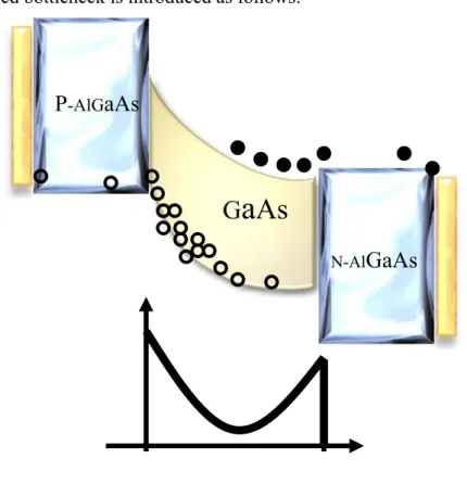
The traditional PIN GaAs PD is refers to that its material of absorption layer is composed by using only GaAs, which may reduce RC bandwidth limitation by increasing thickness of absorption layer. However, such reconstruct increase carrier drift time and lower devices speed and saturation current. In the other side, if we decrease absorption layer to achieve higher saturation current, problems caused such as serious bandwidth limitation and lower quantum efficiency. Moreover, under high input power excitation, too much photo carrier generated may cause the speed slow electricity hole accumulates in inner absorption layer, which will form a built-in field. [25-26] Such built-in field would screen external field and reduce devices speed and
P
-AlGaAs
N-Al
GaAs
G
a
As
Figure 2- 5A schematic drawing of energy band and electric field distributed for traditional GaAs PD under high power excitation
33
output saturation current, which is so-called space charge screen effect. The trade-off problem between RC bandwidth limitation, carrier drift time and saturation current become a complex and hard test while design our devices.
Traditional PIN LT-GaAs based PD
Traditional PIN LTG-GaAs PD stands for its absorption layer are composed of by only low temperature grown GaAs. [24] Because there are lots of defects in LTG-GaAs, drift carrier generated will be captured and recombined, which means short carrier life time as shown in figure 2-8.[27] In other words, speed limitation of devices would transform from carrier drift time to carrier life time, this may improve devices speed a lot. By this method, trade off problem between capacitance bandwidth limitation and carrier drift time will be solved. It also improves space charge effect in this structure under higher input power excitation.
However, because LTG-GaAs in absorption layer is material with short carrier life time, most generated photo-carrier will be recombined and reduce quantum efficiency seriously. In the other side, there are much defects exists in absorption layer which may induce effect like heavy doping in absorption layer while applied external electrical field on the devices Thus depletion layer will exist in the junction layer between absorption layer and conduction layer. As a result, electrical field would be applied in conduction layer and lower internal electrical field in the absorption layer, which may limit carrier speed and limit speed and efficiency of devices.
34
In order to apply electrical field in the absorption area, higher applied voltage on the devices is needed. However, when we apply higher voltage on the absorption area, speed of devices is not e increased as excepted. This is because carrier life time
Normal
Enhanced Electric field
Carrier will be
trapped
Out of shape
Carrier can tunnel off
LTG-GaAs
defects
P-AlGaAs
N-AlGaAs
Figure 2- 6Traditional LTG-GaAs PD energy band diagram and electrical field distribution.
35
increasing effect for LTG-GaAs, which means trap energy will change shape due to column effect under high applied voltage. [29-30] such effect may cause trapped carriers escaped from trap state in tuning mechanism, which means poor recombination effect and poor operation speed.
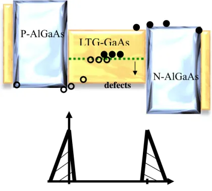
Separated transmission recombined travelling wave PD (STR-PD)
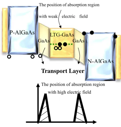
According to above two type traditional photodiode, we can learn trade off problems of speed, efficiency and saturation power will cause problem of design devices. Thus we propose a new type photo diode to solve the problem-- Separated transmission recombined travelling wave photo diode (STR-PD).
P-AlGaAs
N-AlGaAs
LTG-GaAs GaAs GaAsTransport Layer
The position of absorption region with high electric field
Recombination center
The position of absorption region with weak electric field
Figure 2- 8Schematic diagram of energy band and electrical field for STR-PD.
36
We adopt travelling wave photo-diode type in PD’s structure and recombination center (LTG-GaAs) in absorption layer. The STR-PD is composed of inserted LTG-GaAs in intrinsic layer GaAs and shown in figure 2-10.
Principal of STR-PD
Because we insert recombination center (LTG-GaAs) in absorption area, total absorption layer thickness become thinker and thus capacitance smaller. Besides, due to carriers in recombination center with slower speed trapped by defects, we could replace carrier drift time limitation by carrier life time. The higher speed performance is expected for carrier trapped time << carrier life time. The key point is we solved trade off problem between RC value and carrier drift time by inserted LTG-GaAs in traditional PIN PD, which we can improve devices performance a lot.
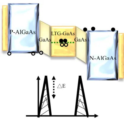
P-AlGaAs
N-AlGaAs
LTG-GaAs GaAs GaAs △EFigure 2- 9 A schematic diagram of electrical field distribution for STR-PD while applied higher external field.
37
Moreover, demanded thickness of conductor layer (intrinsic GaAs) could be thinner due to designed thickness of recombination center, thus higher saturation currier could be expected while operated under this condition. As shown in figure 2-11, higher external electrical field mainly applied in collector layer which located on both side of LTG-GaAs having lots of defects and behavior like heavy doping. External electrical field is avoided to fall into recombination center, which avert life time increasing effect mentioned above under high external electrical field. Besides, under high power excitation, screen effect induced by accumulated electrical holes in absorption area would weaken electrical field in absorption center. However, the recombination center could trap carriers rapidly thus increase speed performance and maximum saturation current under high power excitation.