共␣-SiCO, k ⫽ 3.7) dielectric barrier. This is followed by investigating the improvement in leakage current and breakdown field of the Cu-comb capacitor with a carbon-doped low-k PECVD organosilicate glass (k⫽ 3) as the intermetal dielectric and an ␣-SiCO dielectric film as the Cu cap barrier. The leakage current and breakdown field of Cu-MIS and Cu-comb capacitors are dependent on the species of the dielectric barrier. The Cu-MIS and Cu-comb capacitors with an␣-SiCO dielectric barrier exhibit a leakage current at least three orders of magnitude smaller than those with an amorphous silicon carbide共␣-SiC, k ⫽ 4.4) dielectric barrier at an applied electric field of 1.6 MV/cm between 25 and 250°C. Moreover, the breakdown field of the Cu-MIS and Cu-comb capacitors with an␣-SiCO dielectric barrier, measured at 200°C, are 60 and 25%, respectively, higher than that of the capacitors with an␣-SiC barrier. The decreased leakage current and increased breakdown field of the Cu-MIS and Cu-comb capacitors with an ␣-SiCO dielectric barrier are attributed to the higher density, oxygen-improved film property, non-semiconductor behavior, and lower fringe- or surface-electric field of the␣-SiCO dielectric film.
© 2004 The Electrochemical Society. 关DOI: 10.1149/1.1777510兴 All rights reserved.
Manuscript submitted November 10, 2003; revised manuscript received February 21, 2004. Available electronically August 11, 2004.
The interconnect resistance-capacitance 共RC兲 delay is a domi-nant factor in determining the performance of integrated circuits beyond 0.18m node technology, in which the use of Cu metal and low-k dielectrics is indispensable in the back-end-of-line 共BEOL兲 process. Cu metal reduces the electrical resistance of interconnect lines because of its low electrical resistivity; moreover, Cu line also exhibits a better electromigration resistance than conventional Al-based wires. Low-k dielectrics in the interconnect system reduce the wire capacitance, signal-propagation delay, cross talk noise between metal lines, and power dissipation of integrated circuits. While many low-k (k⬍ 3) materials have been used as inter- and intralayer dielectrics共ILD兲, high dielectric constant (k ⬎ 7) silicon nitride is still the primary candidate for the Cu cap barrier and etching stop layer共ESL兲 required in the Cu damascene structure. It is desirable to replace silicon nitride with dielectric materials of lower k value (k ⬍ 5) to further reduce the effective dielectric constant of the Cu interconnect system. In recent years, amorphous silicon carbide 共␣-SiC兲, amorphous silicon nitricarbide. 共␣-SiCN兲, and amorphous sili-con oxycarbide共␣-SiCO兲 deposited by plasma-enhanced chemical vapor deposition共PECVD兲 using organosilicate gases have received extensive attention for applications as Cu cap-barrier and ESL in Cu interconnection scheme because of their lower k value, better etch-ing selectivity with organosilicate glass共OSG兲, robust chemical me-chanical polishing共CMP兲 strength, good photoresist poisoning re-sistance, higher antireflective ability, and superior properties as a Cu barrier/passivation layer in terms of Cu restraint, electromigration resistance, and Cu hillock density.1-6The fine-tuned␣-SiC is better than␣-SiCN and ␣-SiCO in the aspects of k value, etching selectiv-ity, photoresist poisoning, antireflective coating lithography behav-ior, adhesion strength to Cu and OSG IMD, electrical property, and reliability performance.2,3,7However, the film stress of␣-SiC is ten-sile or less compressive as compared with that of ␣-SiCN and ␣-SiCO, which results in a poor stack stability of Cu-OSG intercon-nect system and a degraded interface quality of␣-SiC/OSG.2,3,8 In this work, we investigated the improvement in leakage current and breakdown field of the copper metal-insulator-semiconductor
共Cu-MIS兲 and Cu-comb capacitors with an ␣-SiCO dielectric barrier over those with an ␣-SiC dielectric barrier having a comparable compressive film stress.
Experimental
The leakage current and breakdown field of MIS and Cu-comb capacitors were measured on the TaN/Cu-gated MIS structure and 0.12/0.12 m 共linewidth/space兲 Cu-OSG single damascene structure, respectively. For the fabrication of Cu-MIS capacitor, 50 nm thick PECVD dielectric films were deposited on p-type, 共100兲-oriented Si wafers at 300-400°C, a gas pressure of 1-5 Torr, and a plasma power of 100-300 W using a parallel-plate system operated at 13.56 MHz. The flow rate ratio of 3MS关(CH3)3SiH兴 precursor with He carrier gas was maintained at 2/5, while the flow rate of CO2 reaction gas was controlled separately at 0 and 1200 sccm, which resulted in the 3MS-based␣-SiC and ␣-SiCO films, respec-tively, with different elemental compositions. A Cu layer, 200 nm thick, was sputter-deposited on the ␣-SiC and ␣-SiCO dielectric films using a dc magnetron sputtering system; this was followed by reactive sputter deposition of a 50 nm thick TaN layer on the Cu surface in the same sputtering system without breaking the vacuum. The TaN film served as a passivation layer to prevent the Cu elec-trode from oxidation in the subsequent high-temperature processes or measurements. The metal electrodes with a circular area of 0.84 mm diameter were defined by a lift-off process to prevent unex-pected deterioration of the dielectric films by chemical wet etching. To ensure good contact in electrical measurements, a 500 nm thick Al layer was thermally evaporated on the back surface of the Si substrate for all samples. The completed Cu-MIS capacitors were thermally annealed at 400°C for 30 min in an N2 ambient. This annealing step eliminates the plasma-induced damage during the sputter deposition of the TaN/Cu electrodes. Figure 1 shows the schematic top and cross-sectional view of the Cu-comb capacitor test structure. A 40 nm PECVD 3MS-based␣-SiCO (k ⫽ 4.5) ESL was deposited on the PECVD oxide ILD. A single level Cu dama-scene共metal 1兲 process with a 250 nm PECVD methylsilane-based carbon-doped low-k OSG as the IMD was employed to fabricate the Cu-comb capacitor. After patterning of 0.12/0.12 m linewidth/ space trenches in the OSG/ESL/ILD dielectric stack, the damascene Cu feature was electrochemically deposited on a 15 nm physical vapor deposited共PVD兲 TaN liner barrier. Following the Cu CMP, *Electrochemical Society Active Member.
the 3MS-based ␣-SiC or ␣-SiCO cap barrier was deposited in a PECVD system. Another layer of PECVD OSG was deposited for the next Cu damascene共metal 2兲 process.
An HP4145B semiconductor parameter analyzer was used to measure the leakage current and breakdown field of the Cu-MIS and Cu-comb capacitors. During the measurement, an N2 purging was used to prevent possible oxidation of the Cu metal and moisture uptake in the dielectric films. Raphael modeling共provided by Avant! business unit兲 was used to obtain the distribution of electric field in the Cu-MIS and Cu-comb capacitors. Auger electron spectroscopy 共AES兲 was used to obtain the chemical composition of the dielectric barrier films. The film thickness and refractive index were measured using an n&k analyzer at 633 nm wavelength, and the k value of the dielectrics was determined by the maximum capacitance of the Al-gated MIS capacitors measured at 1 MHz using a Keithley package 82 C-V measurement system. The film density was calculated di-rectly by the ratio of mass to volume of the film, whereas the film mass was measured by an electronic microbalance and the film vol-ume was calculated by the film thickness and the area of the sub-strate wafer. The film stress was measured using a well-calibrated thin-film stress analyzer.
Results and Discussion
Physical property of␣-SiC and ␣-SiCO.—Table I shows the ba-sic film properties of 3MS-based␣-SiC and ␣-SiCO dielectrics stud-ied in this work. Although the chemical composition indicates that the oxygen content in SiCO is much higher than that in SiC, both dielectrics have nearly the same deposition rate and compressive film stress. The compressive stress of about⫺200 MPa in the SiC and SiCO dielectric films is high enough to achieve a robust stack stability.2,3However, it is conceivable that the SiC may exhibit in-ferior thermal stability and electrical and barrier properties because of its lower density共i.e., higher degree of porosity兲.9,10Nonetheless, the refractive index of the SiCO is lower than that of the SiC; this results in lower electronic-dielectric constant, and thus lower
dielec-tric constant共at 1 MHz兲 of SiCO film because of the replacement of Si-C with Si-O bond and the higher electronegativity of oxygen atom.11
Electrical property of Cu-MIS capacitor.—Figure 2 shows the leakage current of Cu-MIS capacitors with SiC and SiCO dielectrics measured at various temperatures. Generally, the leakage current of the SiCO sample is three orders of magnitude smaller than that of the SiC sample at an electric field of 1.6 MV/cm and at temperatures ranging from 25 to 250°C, presumably due to the higher density of the SiCO film共Table I兲. The higher density 共i.e., lower degree of porosity兲 of film prohibited the diffusion/drift of Cu owing to the miniature free volume.10,12-16Higher oxygen content in the␣-SiCO dielectric film would also effectively reduce the film leakage current.17 Because single-crystal SiC is a semiconductor with a bandgap of 2.3-3.0 eV, the polycrystal or amorphous SiC possibly also has a semiconductor nature of high conductivity. Therefore, it is natural to reduce the leakage current of SiC by doping with oxygen and making SiCO. From the log-log plot of the leakage current vs. electric field data, two different electric-field-dependent conduction mechanisms are observed in the MIS capacitors. First, all Cu-MIS capacitors exhibit ohmic conduction at low electric fields共⬍0.3 and⬍1 MV/cm for SiC and SiCO, respectively兲 because the leak-age current共I兲 is linearly correlated with the electric field 共E兲,18and the current can be expressed by Eq. 1.19The ohmic conduction is carried by thermally excited electrons hopping from one isolated
Figure 1. Schematic共a兲 top view and 共b兲 cross-sectional view of the
Cu-comb capacitor test structure.
Table I. Basic film properties for 3MS-based␣-SiC and ␣-SiCO dielectric barriers 50 nm thick used in this study.
Sample ID SiC SiCO
Structure ␣-SiC ␣-SiCO
Chemical composition SiC0.92O0.04 SiC0.97O0.66
Deposition rate共nm/min兲 100.4 102.6
Film stress共MPa兲 ⫺200 ⫺210
Film density共g/cm3兲 1.24 1.80
Refractive index at 633 nm 2.04 1.72
Dielectric constant at 1 MHz 4.41 3.73
Figure 2. Leakage current density vs. electric field in a log-log plot,
mea-sured at various temperatures, for Cu-MIS capacitors with共a兲 ␣-SiC and 共b兲
␣-SiCO dielectric films.
state to the next.18,19However, at high electric fields共⬎0.3 and ⬎1 MV/cm for SiC and SiCO, respectively兲, the Cu-MIS capacitors with SiC and SiCO dielectrics exhibit different slopes in their I-E plot, particularly above 200°C. This implies that the SiC and SiCO samples have different conduction mechanisms at high electric fields. From some replots of the known conduction mechanisms in dielectrics,18,19we found that the SiC sample exhibits Frenkel-Poole 共F-P兲 emission, while the SiCO sample reveals Schottky emission 共SE兲, as shown in Fig. 3. The F-P emission shows Ln(I/E) linearly correlated with E1/2共Fig. 3a兲, and the current can be expressed by Eq. 2.18,19The SE conduction shows Ln(I/T2) linearly correlated with E1/2共Fig. 3b兲, and the current can be expressed by Eq. 3.19The F-P emission is due to field-enhanced thermal excitation of trapped electrons in the dielectrics into the conduction band, while the SE conduction is derived from the thermionic emission across the metal-dielectric interface or the dielectric-semiconductor interface18-20
Ohmic I ⬃ E exp共⫺⌬Eae/kT兲 关1兴
FP I⬃ E exp共2E1/2/kT⫺ q⌽B/kT兲 关2兴
SE I⬃ T2exp共E1/2/kT ⫺ q⌽
B/kT兲 关3兴
where ⌬Eae is the activation energy of electron,  represents (q3/4)1/2, and is the dielectric dynamic permittivity, k is the Boltzmann constant, q is an electron charge, and⌽FPis the barrier height of trap potential well, and⌽SEis the barrier height of metal/ dialectric interface.19The F-P emission and higher leakage current of the SiC sample are presumably due to the presence of defects and/or traps18-20 possibly resulting from the film lower density. Clearly, temperature enhances the F-P emission and SE conduction in the SiC and SiCO samples, respectively共Fig. 3兲. Figure 4 shows the leakage current and breakdown field for the SiC and SiCO Cu-gated MIS capacitors measured at 200°C. The measurements were performed with the MIS capacitors biased in the accumulation re-gion. The breakdown field is defined as the field strength such that the leakage current of the MIS capacitor reaches the current limit of the HP4145B semiconductor parameter analyzer. Notably, the breakdown field of the SiCO sample is about 60% higher than that of the SiC sample. This increase in breakdown field is presumably due to the enhanced Si-O bond that has a high thermochemical energy.21Moreover, the oxygen atoms and the higher density of the SiCO dielectric film would also effectively increase the breakdown field.11,18 In addition, the lower k value of the SiCO film would induce lower fringe-electric field around the metal-gate corner, as illustrated in the model shown in Fig. 5, which is derived from the high-k gate dielectrics used in the front-end-of-line 共FEOL兲 technology.22It is conceivable that the lower fringe-electric field in the SiCO film would result in lower leakage current and higher breakdown field for the SiCO sample.
Figure 3. Conduction mechanism of共a兲 Frenkel-Poole emission in TaN/Cu/ ␣-SiC/Si and 共b兲 Schottky emission in TaN/Cu/␣-SiCO/Si samples.
Figure 4.共a兲 Leakage current density vs. electric field and 共b兲 distribution of
breakdown field for the␣-SiC and ␣-SiCO Cu-gated MIS capacitors mea-sured at 200°C.
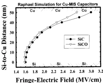
Figure 6 shows the fringe-electric field obtained from Raphael simu-lation for the Cu-gated MIS capacitors of SiC as well as SiCO dielectric biased with an electric voltage of 10 V, which would pro-duce an electric field of 2 MV/cm in the dielectric layer of the Cu-MIS capacitor. Notably, the SiC sample exhibits about 10% in-crease of fringe-electric field near the Cu electrode as compared with the SiCO sample.
Electrical property of Cu-comb capacitor.—Figure 7 shows the leakage current, measured at various temperatures, for the Cu-comb capacitors with SiC as well as SiCO dielectric cap barriers. Notably, the dependence of leakage current on the cap barrier dielectric ma-terial implies that the dominant leakage paths are not in the bulk OSG but in the bulk cap barrier and along the cap barrier/OSG interface共CMP surface兲.23,24That the leakage current of the SiCO sample at a field of 1.6 MV/cm between 25 and 250°C is at least three orders of magnitude smaller than that of the SiC sample, may be attributed to the semiconductor nature of SiC and the better elec-trical property of the SiCO film, as studied in the previous paragraph using the MIS capacitors. Moreover, the CMP surface leak-path may be efficiently eliminated in the SiCO sample because both the SiCO
cap barrier and the OSG layer are similar materials of Si-C-O pounds, while the SiC cap barrier is an oxygen-absent Si-C com-pound. Similar presumption was reported for the CMP surface at the ␣-SiCN 共cap barrier兲/␣-SiCN 共hard mask兲 interface of the same ma-terial in the Cu damascene interconnect.23 Two different electric-field-dependent conduction mechanisms were also observed in the Cu-comb capacitors. First, all Cu-comb capacitors exhibit ohmic conduction at low electric fields共⬍0.3 and ⬍0.4 MV/cm for SiC and SiCO cap barriers, respectively兲 because the leakage current 共I兲 is linearly correlated with the electric field共E兲.18,19Nevertheless, at high electric fields共⬎0.3 and ⬎0.4 MV/cm for SiC and SiCO cap barriers, respectively兲, the Cu-comb capacitors with SiC and SiCO cap barriers exhibit quite different nonlinear I-E relation, particu-larly at temperatures above 200°C. This implies that the SiC and SiCO samples have different conduction mechanisms at high elec-tric fields. From the best fitting of the known conduction mecha-nisms in dielectrics,18,19we found that the SiC sample exhibits F-P emission, while the SiCO sample reveals SE conduction, as shown in Fig. 8. The Cu-comb capacitors and the Cu-MIS capacitors ex-hibit the same electric-field-dependent conduction mechanisms. This further confirms that the dominant leakage paths are not only along the cap barrier/OSG interface共CMP surface兲 but also in the bulk cap barrier. Furthermore, in our previous work the more leaked CMP surface of Cu-comb capacitor also enhanced the leakage current and F-P emission.8 Thus, the semiconductor nature of the conductive bulk SiC and the more leaked CMP surface at the SiC/OSG interface resulted in the increased leakage current and F-P emission for the
Figure 5. Proposed fringe-electric field in the MIS capacitor.
Figure 6. Fringe-electric field obtained from Raphael simulation for the
Cu-gated MIS capacitors of␣-SiC as well as ␣-SiCO dielectric biased with an electric voltage of 10 V共equivalent to an electric field of 2 MV/cm兲.
Figure 7. Leakage current vs. electric field in a log-log plot, measured at
various temperatures, for Cu-comb capacitors with共a兲 ␣-SiC and 共b兲 ␣-SiCO cap barriers.
Cu-comb capacitor with a SiC cap barrier. Figure 9 shows the leak-age current and breakdown field for the Cu-comb capacitors with SiC and SiCO dielectric cap barriers measured at 200°C. Notably, the breakdown field of the SiCO sample is about 25% higher than that of the SiC sample. This increase in breakdown field is presum-ably due to the better electrical property of bulk SiCO and the dimi-nution of CMP-surface leak-path. In addition, the lower k value of the SiCO film also reduces the surface-electric field at the cap barrier/OSG interface共CMP surface兲, as illustrated in Fig. 10.24,25 The lower surface-electric field at the CMP surface results in a lower leakage current and higher breakdown field for the SiCO sample. Figure 11 shows the surface-electric field obtained from Raphael simulation for the Cu-comb capacitors biased with an electric volt-age of 24 V, which produces an electric field of 2 MV/cm in the dielectric layer of the Cu-comb capacitor. Notably, the surface-electric field near the Cu line of the SiCO sample is about 6% lower than that of the SiC sample.
Conclusion
The leakage current and breakdown field of the Cu-MIS and Cu-comb capacitors are dependent on the dielectrics 共␣-SiC and
␣-SiCO兲 used as insulator and dielectric cap barrier, respectively. The Cu-MIS and Cu-comb capacitors with an ␣-SiCO (k ⫽ 3.7) dielectric barrier exhibit a leakage current at least three orders of Figure 8. Conduction mechanism of共a兲 Frenkel-Poole emission in Cu-comb
capacitor with␣-SiC cap barrier and 共b兲 Schottky emission in Cu-comb capacitor with␣-SiCO cap barrier.
Figure 9. 共a兲 Leakage current vs. electric field and 共b兲 distribution of
break-down field for the ␣-SiC and ␣-SiCO Cu-comb capacitors measured at 200°C.
magnitude smaller than those with an␣-SiC (k ⫽ 4.4) dielectric barrier at an applied electric field of 1.6 MV/cm between 25 and 250°C. Moreover, the breakdown field of the Cu-MIS and Cu-comb capacitors with an␣-SiCO dielectric barrier, measured at 200°C, are 60 and 25%, respectively, higher than that of the capacitors with an ␣-SiC barrier. The decreased leakage current and increased break-down field of the Cu-MIS and Cu-comb capacitors with an␣-SiCO dielectric barrier are attributed to the higher density, oxygen-improved film property, non-semiconductor behavior, and lower fringe- or surface-electric field of the␣-SiCO dielectric film.
Acknowledgment
The authors express their gratitude to Dr. Chih-Feng Huang of National Chiao-Tung University for his valuable help of Raphael simulation.
National Chiao-Tung University assisted in meeting the publication costs of this article.
References
1. F. Lanckmans, W. D. Gray, B. Brijs, and K. Maex, Microelectron. Eng., 55, 329 共2001兲.
2. K. Goto, H. Yuasa, A. Andatsu, and M. Matsuura, in Proceedings of IEEE 2003
IITC, p. 6共2003兲.
3. M. Fayolle, J. Torres, G. Passemard, F. Fusalba, G. Fanget, D. Louis, L. Arnaud, V. Girault, J. Cluzel, H. Feldis, M. Rivoire, O. Louveau, T. Mourier, and L. Brous-sous, in Proceedings of IEEE 2002 IITC, p. 39共2002兲.
4. J. Martin, S. Filipiak, T. Stephens, F. Huang, M. Aminpur, J. Mueller, E. Demircan, L. Zhao, J. Werking, C. Goldberg, S. Park, T. Sparks, and C. Esber, in Proceedings
of IEEE 2002 IITC, p. 42共2002兲.
5. T. Ishimaru, Y. Shioya, H. Ikakura, M. Nozawa, Y. Nishimoto, S. Ohgawara, and K. Maeda, in Proceedings of IEEE 2001 IITC, p. 36共2001兲.
6. K. I. Takeda, D. Ryuzaki, T. Mine, and K. Hinode, in Proceedings of IEEE 2001
IITC, p. 244共2001兲.
7. C. C. Chiang, M. C. Chen, Z. C. Wu, L. J. Li, S. M. Jang, C. H. Yu, and M. S. Liang, in Proceedings of IEEE 2002 IITC, p. 200共2002兲.
8. C. C. Chiang, I. H. Ko, M. C. Chen, Z. C. Wu, Y. C. Lu, S. M. Jang, and M. S. Liang, in Proceedings of IEEE 2003 IITC, p. 201共2003兲.
9. J. Y. Kim, M. S. Hwang, Y. H. Kim, H. J. Kim, and Y. Lee, J. Appl. Phys., 90, 2469 共2001兲.
10. Z. C. Wu, Z. W. Shiung, C. C. Chiang, W. H. Wu, M. C. Chen, S. M. Jeng, W. Chang, P. F. Chou, S. M. Jang, C. H. Yu, and M. S. Liang, J. Electrochem. Soc.,
148, F127共2001兲.
11. Y. W. Koh, K. P. Loh, L. Rong, A. T. S. Wee, L. Huang, and J. Sudijono, J. Appl.
Phys., 93, 1241共2003兲.
12. A. L. S. Loke, J. T. Wetzel, P. H. Townsend, T. Tanabe, R. N. Vrtis, M. P. Zussman, D. Kumar, C. Ryu, and S. S. Wong, IEEE Trans. Electron Devices, 46, 2178 共1999兲.
13. D. Gupta, Mater. Chem. Phys., 41, 199共1995兲.
14. J. D. Mcbrayer, R. M. Swanson, and T. W. Sigmon, J. Electrochem. Soc., 133, 1242 共1986兲.
15. J. L. Duda and N. Faridi, Diffusion in Amorphous Materials, H. Jain and D. Gupta, Editors, The Minerals, Metals and Materials Society, Warrendale, PA, p. 55共1994兲. 16. D. Gupta, F. Faupel, and R. Willecke, Diffusion in Amorphous Materials, H. Jain and D. Gupta, Editors, The Minerals, Metals and Materials Society, Warrendale, PA, p. 189共1994兲.
17. T. Ishimaru, Y. Shioya, H. Ikakura, M. Nozawa, S. Ohgawara, T. Ohdaira, R. Suzuki, and K. Maeda, J. Electrochem. Soc., 150, F83共2003兲.
18. D. Brassard and M. A. E. Khakani, J. Appl. Phys., 93, 4066共2003兲.
19. S. M. Sze, Physics of Semiconductor Devices, 2nd ed., p. 403, John Wiley & Sons, New York共1981兲.
20. P. T. Liu, T. C. Chang, Y. L. Yang, Y. F. Cheng, and S. M. Sze, IEEE Trans.
Electron Devices, 47, 1733共2000兲.
21. J. R. Bowser, Inorganic Chemistry, p. 401, Brooks/Cole Publishing Co., Pacific Grove, CA共1993兲.
22. G. C. F. Yeap, S. Krishnan, and M. R. Lin, IEEE Electron Device Lett., 34, 1150 共1998兲.
23. M. Tada, Y. Harada, H. Ohtake, S. Saito, T. Onodera, and Y. Hayashi, in
Proceed-ings of IEEE 2003 IITC, p. 256共2003兲.
24. J. Noguchi, T. Saito, N. Ohashi, H. Ashihara, H. Maruyama, M. Kubo, H. Yamagu-chi, D. Ryuzaki, K. I. Takeda, and K. Hinode, in Proceedings of IEEE 2001 IRPS, p. 355共2001兲.
25. Z. C. Wu, T. J. Chou, S. H. Lin, Y. L. Huang, Y. L. Yang, L. P. Li, B. T. Chen, Y. C. Lu, C. C. Chiang, M. C. Chen, W. Chang, S. M. Jang, and M. S. Liang, Tech.
Dig. - Int. Electron Devices Meet., To be published. Figure 11. Surface-electric field obtained from Raphael simulation for the
Cu-comb capacitors with␣-SiC and ␣-SiCO cap barrier biased with an elec-tric voltage of 24 V共equivalent to an electric field of 2 MV/cm兲.