Improved Performance of MIC Poly-Si TFTs Using Driven-in Nickel Induced Crystallization (DIC) with Cap SiO2 by F implantation
Ming-Hui Lai, YewChung Sermon Wu, Teng-Fu Tung and Hung-Yu Wu Department of Materials Science and Engineering, National Chiao Tung University,
Hsinchu 300, Taiwan, Republic of China
A cap oxide layer was employed to substantially decrease nickel
residues and passivate the trap states of the devices. F+
implantation was used to drive Ni in α-Si layer to induce crystallization (DIC) process with cap oxide to reduce Ni concentration and minimize the trap-state density. As a result, DIC-TFT with cap oxide exhibit higher field-effect mobility, lower subthreshold slope, lower threshold voltage, higher on/off current ratio, and lower trap-state density (Nt) compared with conventional
MIC TFTs.
Introduction
Low-temperature polycrystalline silicon thin-film transistors (LTPS-TFTs) have attracted considerable interest for their use in active-matrix liquid crystal displays
(AMLCD). MIC is an effective method to obtain high-quality LTPS bellow 600oC.
However, Ni and NiSi2 precipitates were trapped in the poly-Si grain boundaries, which
increase the leakage current and shift the threshold voltage (1, 2). Therefore, it is important to reduce Ni contamination to enhance the performance of the device. Furthermore, several studies have demonstrated the use of fluorine-ion implantation to improve the device performance because Si-F bond is stronger to show a better stability. Unfortunately, the leakage current, the most important character of MIC/MILC TFTs performance, was not decreased with the passivation process (3).
In this study, a cap oxide layer was employed to substantially decrease nickel residues and passivate the trap states of the devices. F+ implantation was used to drive Ni in α-Si
layer to induce crystallization (DIC) process with cap oxide to reduce Ni concentration and minimize the trap-state density.
Experimental
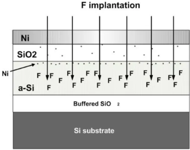
N-type self-alignment poly-Si TFTs were investigated in this study. A 100-nm-thick undoped α-Si layer was deposited onto a 500-nm-thick oxide-coated Si wafer by low pressure chemical vapor deposition (LPCVD) system. The 5-nm-thick cap oxide layer was formed by a simple chemical method (4). A 5-nm-thick Ni film was then deposited. Samples were subjected to F+ implantation to drive Ni in the α-Si layer, as shown in Fig.1.
The projection range was set at the 15 nm of depth near cap oxide/α-Si layer interface.
The ion-accelerating energy and dosage was 13 KeV and 2×1015 cm-2, respectively. To
reduce the Ni contamination, the remained Ni film and cap oxide layer were then
removed by wet etching, and subsequently annealedat 500°C for 1 h in N2 to form
poly-Si films. The islands of poly-poly-Si regions were defined by Reactive ion etching (RIE). Next, a 100-nm-thick α-Si as a gate insulator was deposited by PECVD. Then a 100-nm-thick poly-Si film was deposited as the gate electrode by LPCVD. After defining the gate, self-aligned 30 keV phosphorous ions were implanted at a dose of 5 × 1015 cm-2 to form the
ECS Transactions, 28 (1) 405-407 (2010) 10.1149/1.3375628 © The Electrochemical Society
405 ecsdl.org/site/terms_use) unless CC License in place (see abstract). address. Redistribution subject to ECS terms of use (see
140.113.38.11
source/drain and gate. Dopant activation was performed at 600°C in N2 ambient for 12 h.
It is worthy to note that this DIC process does not need any additional annealing step and is compatible with MIC processes.
RESULTS AND DISCUSSION
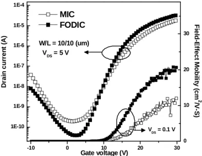
Fig. 2 shows the ID–VG transfer characteristics at a drain bias of 5 V for 10 × 10 μm2
devices with and without FODIC treatment. The measured and extracted key device
parameters are summarized in Table I. The threshold voltage (Vth) is defined at a
normalized drain current of IDS = (W/L) × 100nA at VDS = 5V. The field-effect mobility
(μFE) is extracted from the maximum value of transconductance at VD = 0.1V. The
electrical characters of DIC-TFTs with cap oxide are significantly improved, in particular
the leakage current of 0.39 pA/μm and the on/off current ratio of 8.72 × 10⁵. Compared
with conventional MIC-TFTs, it shows 4.97-fold decreasing in the leakage current and 8.93-fold in the on/off current ratio. The leakage current improvement was attributed to lower nickel concentration in the DIC poly-Si films. In the poly-Si film, nickel residues serve as deep-level traps to dominate thermionic-emission leakage current in the low-gate and drain-voltage region (5, 6). From the SIMS data, cap oxide might reduce content of Ni into channel layer during driven-in process to conspicuously decrease leakage current. In addition, FODIC-TFT shows higher on-current than MIC-TFT. The trap state density (Nt) of MIC-TFT and FODIC-TFT was extracted using Levinson and Proano’s method
(7). It was found that MIC-TFT exhibits a Nt of 5.69 × 1012 cm-2, whereas FODIC-TFT
was 5.24 ×1012 cm-2. The reduction in Nt values implies that those defects have been
effectively terminated using F+ implantation. Therefore, the carrier mobility increases due to decrease in the boundary scattering by passivation of grain boundaries defects.
Summary
The cap oxide between Ni and α-Si layer led to Ni content much lower than F+ implant
dosage, so that the Ni induced leakage current was decreased and F+ passivation effect
was increased. The electrical performance of FODIC-TFTs was improved substantially due to low content of nickel and passivation of fluorine-ion in the poly-Si films.
Fig. 1 The key process of poly-Si TFT device.
ECS Transactions, 28 (1) 405-407 (2010)
406 ecsdl.org/site/terms_use) unless CC License in place (see abstract). address. Redistribution subject to ECS terms of use (see
140.113.38.11
-10 0 10 20 30 1E-10 1E-9 1E-8 1E-7 1E-6 1E-5 1E-4 W/L = 10/10 (um) VDS = 5 V MIC FODIC Fiel d-Ef fe c t M obi lit y ( c m 2 /V -S ) Gate voltage (V) D rai n cu rr e n t ( A ) 0 10 20 30 V DS = 0.1 V
Fig. 2 Typical IDS-VGS transfer characteristics and filed-effect mobility.
TABLE I. Device characteristics of the MIC-TFTs and FODIC-TFTs
Device Parameters MIC FODIC
Field-Effect Mobility μFE (cm2 / V-s) 13.22 21.18
Threshold Voltage Vth (V) 12.96 12.10
Subthreshold Slope S.S (V / dec) 2.72 2.03
Imin (pA/μm) 1.94 0.39
Max on/off ratio (×105) 0.98 8.72
Acknowledgments
This project was funded by Sino American Silicon Products Incorporation and the NSC of the ROC under Grant No. 98-2221-E-009-041-MY3. Technical supports from the National Nano Device Laboratory, Center for Nano Science and Technology and the Nano Facility Center of the National Chiao Tung University are also acknowledged.
References
1. P. J. van der Zaag, M. A. Verheijen, S. Y. Yoon, and N. D. Young, Appl. Phys.
Lett., 81, 3404 (2002).
2. G. A. Bhat, H. S. Kwok, and M. Wong, Solid State Electron., 44, 1321 (2000). 3. C. P. Chang and Y. C. Sermon Wu, IEEE Electron Device Lett., 28, 990 (2007). 4. B. M. Wang and Y. C. Sermon Wu, Electrochem. Solid-State Lett., 12, J14 (2009). 5. K. R. Olasupo and M. K. Hatalis, IEEE Trans. Electron Devices, 43, 1218 (1996). 6. C. A. Dimitriadis, P. A. Coxon, L. Dozsa, L. Papadimitriou, and N. Economou,
IEEE Trans. Electron Devices, 39, 598 (1992).
7. J. Levinson, G. Este, M. Rider, P. J. Scanlon, F. R. Shepherd, and W. D Westwood. J. Appl. Phys. 53, 1193 (1982).
ECS Transactions, 28 (1) 405-407 (2010)
407 ecsdl.org/site/terms_use) unless CC License in place (see abstract). address. Redistribution subject to ECS terms of use (see
140.113.38.11