Role of extrinsic atoms on the morphology and field emission properties of carbon
nanotubes
L. H. Chan, K. H. Hong, D. Q. Xiao, W. J. Hsieh, S. H. Lai, H. C. Shih, T. C. Lin, F. S. Shieu, K. J. Chen, and H. C. Cheng
Citation: Applied Physics Letters 82, 4334 (2003); doi: 10.1063/1.1579136 View online: http://dx.doi.org/10.1063/1.1579136
View Table of Contents: http://scitation.aip.org/content/aip/journal/apl/82/24?ver=pdfcov Published by the AIP Publishing
Articles you may be interested in
Growth of multiwalled-carbon nanotubes using vertically aligned carbon nanofibers as templates/scaffolds and improved field-emission properties
Appl. Phys. Lett. 86, 053110 (2005); 10.1063/1.1852730
Growth of Aligned Multiwall Carbon Nanotubes and the Effect of Adsorbates on the Field Emission Properties AIP Conf. Proc. 685, 605 (2003); 10.1063/1.1628100
Field emission of aligned grown carbon nanotubes AIP Conf. Proc. 685, 550 (2003); 10.1063/1.1628091
Effect of length and spacing of vertically aligned carbon nanotubes on field emission properties Appl. Phys. Lett. 82, 3520 (2003); 10.1063/1.1576310
Field-emission properties of vertically aligned carbon-nanotube array dependent on gas exposures and growth conditions
J. Vac. Sci. Technol. A 19, 1786 (2001); 10.1116/1.1372915
This article is copyrighted as indicated in the article. Reuse of AIP content is subject to the terms at: http://scitation.aip.org/termsconditions. Downloaded to IP: 140.113.38.11 On: Wed, 30 Apr 2014 06:55:18
Role of extrinsic atoms on the morphology and field emission properties
of carbon nanotubes
L. H. Chan, K. H. Hong, D. Q. Xiao, W. J. Hsieh, S. H. Lai, and H. C. Shiha)
Department of Materials Science and Engineering, National Tsing Hua University, Hsinchu, Taiwan 300, Republic of China
T. C. Lin and F. S. Shieu
Department of Materials Engineering, National Chung Hsing University, Taichung, Taiwan 402, Republic of China
K. J. Chen and H. C. Cheng
Department of Electronics Engineering, National Chiao Tung University, Hsinchu, Taiwan 300, Republic of China
共Received 7 November 2002; accepted 11 April 2003兲
Extrinsic atoms were doped into multiwalled carbon nanotubes 共MWCNTs兲 using microwave plasma-enhanced chemical vapor deposition. Doped nitrogen atoms alter the original parallel graphenes into highly curved ones including some fullerene-like structures. Doped nitrogen atoms could replace carbon atoms in MWCNTs and therefore increase the electronic density that enhances the electron field emission properties. On the other hand, the incorporation of boron into the carbon network apparently increases the concentration of electron holes that become electron traps and eventually impedes the electron field emission properties. Fowler–Nordheim plots show two different slopes in the curve, indicating that the mechanism of field emission is changed from low to high bias voltages.values could be increased by an amount of 42% under low bias voltages and 60% under high bias voltages in the N-doped MWCNTs, but decreased by an amount of 8% under low bias region and 68% under high bias voltage in the B-doped MWCNTs. © 2003 American
Institute of Physics. 关DOI: 10.1063/1.1579136兴
Carbon nanotubes共CNTs兲 have drawn great attention in the whole scientific world for their superior electronic prop-erties as an electron source for field emission display.1,2The characteristic aspect ratio contributes to the excellent field emission behaviors such as much smaller turn-on voltage and larger emission current density than any other field emis-sion devices. In the Fowler–Nordheim3coordinates, field en-hancement factor  could provide an indicatively physical factor to investigate and compare the results. Similar to other semiconductor materials, extrinsic doping of CNTs could al-ter and adjust the electronic properties and binding configu-rations of the CNTs. It is known that the boron-doped nano-tubes are intrinsically metallic by the theoretical calculations4and conductivity measurements.5In this work, both nitrogen and boron atoms are separately doped into multiwalled CNTs 共MWCNTs兲 by a microwave plasma-enhanced chemical vapor deposition共MPECVD兲 apparatus6 and the influence of doped atoms on the field emission phe-nomena is discussed and compared.
MWCNTs were synthesized by the assistance of electro-plated Pd catalyst7on the tungsten substrate in a MPECVD apparatus with a mixture of methane and hydrogen as precursors.8 The microwave was generated at the frequency of 2.45 GHz by magnetron and 2.1 kW was used to synthe-size MWCNTs. An external dc bias voltage of ⫺350 V was simultaneously applied to the substrate and the synthesis temperature of the substrate was 600– 700 °C. The vacuum system was maintained at 14 Torr under the mixed methane
and hydrogen atmosphere. In order to dope nitrogen atoms, MWCNTs were further exposed to nitrogen plasma of 3.1 kW microwave input for 30 min. The B-doped CNTs were produced by a mixture of CNTs and HBO3powder under the
hydrogen plasma in the MPECVD system. The carbon-based nanostructures were characterized by transmission electron microscopy 共TEM兲, and the chemical analysis was carried out by x-ray photoelectron spectroscopy 共XPS兲. The atomic ratio of the relevant elements was obtained by integrating the core-level peak area, calibrated by the atomic sensitivity factor.9The electron field emission properties were measured by a conventional diode method at a pressure of 5
⫻10⫺6 Torr. The Keithley 237 instrument was employed to
measure the current density and electric field characteristics. Indium tin oxide glass was made as the anode to receive the emitted electrons with a spacer of 150 m coverglass to separate from the cathode. The emitted area was fixed at 1 cm2. The voltage was increased by a step of 10 V/s from 0 to 1100 V. Before the measurement, a voltage of 0–300 V was applied several times to remove contamination adsorbed on tips.
In the total energy calculations using semiempirical Hartree–Fock-based AM1 method,10,11 the incorporation of nitrogen into graphite-like structures would introduce penta-gon defects in the hexapenta-gon network. The formation of pen-tagon would distort and bend the graphite layers, leading to graphenes with high curvatures and cross-linked structures. In addition, basal planes of the graphite layers appear buck-led, bent and frequently interlinked. It was also proposed that the fullerene-like structures are able to form in the carbon nitride matrix.12 In the study of TEM analysis, the basal
a兲Author to whom correspondence should be addressed; electronic mail:
APPLIED PHYSICS LETTERS VOLUME 82, NUMBER 24 16 JUNE 2003
4334
0003-6951/2003/82(24)/4334/3/$20.00 © 2003 American Institute of Physics
This article is copyrighted as indicated in the article. Reuse of AIP content is subject to the terms at: http://scitation.aip.org/termsconditions. Downloaded to IP: 140.113.38.11 On: Wed, 30 Apr 2014 06:55:18
planes of the graphenes are straight and parallel in the cylin-drical MWCNTs, as shown in Fig. 1共a兲. When nitrogen at-oms were doped into CNTs, original ordered parallel layers of the walls are disturbed and highly curved. Consequently some fullerene-like structures also form, as seen in Fig. 1共b兲. It shows that all the graphene layers of CNTs are affected and appear seriously distorted, similar to the fingerprints of human being.
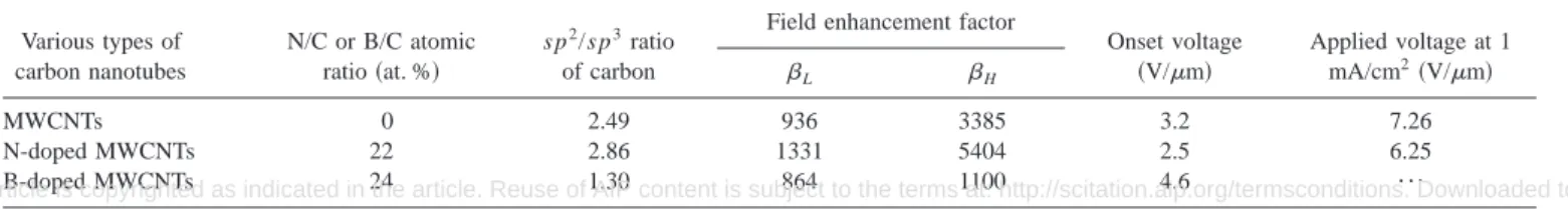
The N (1s) and B (1s) core binding energies are de-tected in the XPS studies. The binding energy around 398 – 401 eV is corresponding to the nitrogen binding configurations.13,14On the basis of the XPS results, the cal-culated N/C ratio is 22 at. % and B/C ratio is 24 at. %共Table I兲. In order to evaluate the sp2/s p3ratio of the carbon atoms, we chose to adopt the method of Marten9 to fit the curve of C (1s) core level binding energy. C1 共284.4 eV兲 is assigned
as the adventitious carbon and surface free carbon, while C4 共290.3 eV兲 is identified as the signal resulting from CO type
bonds. The s p2/s p3 ratio could be estimated by the method
of dividing the integrated peak area of C2 共285.6 eV兲 by the
peak area of C3 共287.6 eV兲. 15
The results are listed in Table I.
Figure 2 is the field emission results of the three types of CNTs and the relevant Fowler–Nordheim plot is shown in the inserted diagram. Because the work function ⌽ of MWCNTs is difficult to measure, it is assumed to be 4.7 eV according to the work function of pure graphite layers 共5 eV兲, and the field enhancement factor  can be calculated from the slope of the straight line in the Fowler–Nordheim
共F–N兲 plot. It is found that there are two straight lines on the
F–N plot andcan be divided into two regions:LandH
under low and high bias voltages, respectively. At low bias voltages, the field emission mechanism obeys the properties of the traditional Fowler–Nordheim equation, while the field emission behavior under high bias voltages deviates from the Fowler–Nordheim equation but still appears a linear rela-tionship on the F–N coordinate. The origin of the deviation from the F–N plot under high bias voltages has long been discussed, and it is commonly explained by the space-charge effect, the presence of localized states at the tip of the emit-ter, interaction between nanotubes and gas desorption/ adsorption on tips.16 –19 The corresponding field emission properties of the different types of CNTs are all compared in Table I. The field emission properties of N-doped CNTs with low onset voltage共2.5 V/m兲 and high emission current den-sity (0.4 mA/cm2 at 5 V/m兲 are superior to other types of CNTs.
FIG. 1. High-resolution TEM images of 共a兲 MWCNT, and 共b兲 N-doped MWCNT by MPECVD. It is shown that the graphene layers of nitrogen doped MWCNTs appear seriously twisted such as turbostratic graphite lay-ers and otherwise contain some fullerene-like structures inside.
TABLE I. Relevant atomic ratios, s p2/s p3ratios, field enhancement factor (LandH), onset voltage, and applied voltage at 1 mA/cm
2
for CNTs doped with nitrogen and boron.
Various types of carbon nanotubes N/C or B/C atomic ratio共at. %兲 s p2/s p3ratio of carbon
Field enhancement factor
Onset voltage 共V/m兲 Applied voltage at 1 mA/cm2共V/m兲 L H MWCNTs 0 2.49 936 3385 3.2 7.26 N-doped MWCNTs 22 2.86 1331 5404 2.5 6.25 B-doped MWCNTs 24 1.30 864 1100 4.6 ¯
FIG. 2. I – V curves of CNTs for field emission measurements and the in-sertion for the Fowler–Nordheim plot. The detail field emission properties are listed in Table I.
4335
Appl. Phys. Lett., Vol. 82, No. 24, 16 June 2003 Chanet al.
This article is copyrighted as indicated in the article. Reuse of AIP content is subject to the terms at: http://scitation.aip.org/termsconditions. Downloaded to IP: 140.113.38.11 On: Wed, 30 Apr 2014 06:55:18
When nitrogen atoms incorporated into graphite-like ma-terials, it is easy for them to substitute carbon atoms in the hexagon graphite network due to the small difference of atomic radii for these two atoms. One excess electron is sup-plied when one nitrogen atom replaces one carbon atom, and the electron concentration in the conduction band can be increased by nitrogen doping into CNTs. The field emission current density is a function of both the tunneling probability of electron depending on the shape of the barrier, and elec-tron supply function depending on the elecelec-tron concentration in the conduction band. For CNTs, increasing electron con-centration is an effective way to enhance the emission prop-erties. N-doped CNTs have even superior emission properties than CNTs. In B-doped CNTs, boron can also replace carbon in the graphite network but produces electron holes in the band structure, which serve as electron traps to make recom-bination with electron and prevent electron from escaping the CNTs. Both generation of holes and recombination effect can decrease electron supply during emission test, thereby leading to a higher onset voltage 共4.6 V/m兲, and lower emission current density (0.1 mA/cm2 at 5.8 V/m兲.
In conventional field emitters,  depends on structure geometry of the device, such as the tip radius of curvature, emitter height, statistical distribution of the tip sharpness and so on.20 But for nanotubes, many reports proposed that  could be affected by other mechanisms in addition to the geometry effect. Because the work function of CNTs is as-sumed to be a fixed value共4.7 eV兲, variation of could be sometimes attributed to other reasons than merely the geom-etry effect.21,22For N-doped CNTs, nitrogen atoms transform concentric graphene cylinders into much more curved and bending layers with some fullerene-like structures inside
关Fig. 1共b兲兴. These locally distorted positions with high
cur-vatures are effective sites to emit electrons. The field ampli-fication effect in these sites is stronger than other smooth places, and  can be enhanced by these sites, such that the N-doped CNTs can have both higherLandHthan CNTs. In addition, binding configuration and local density of states can also have influence on the field emission behaviors. By
ab initio pseudopotential electronic structure calculation for
several edge geometries of the (n, n) single-wall nanotubes,23 the capped nanotube with-bonding states lo-calized at the cap and pointing in the tube axis direction are favorable for field emission. In some cases such as pyramidal diamond tips,24 field emission characteristics can be en-hanced by increasing the s p2contents. In the studies of car-bon nitride materials, it is known that nitrogen atoms could assist the formation of s p2 bonding by reducing the total energy and approaching more stable states by ab initio HF and DF calculations with B3LYP/6-31G共d兲//HF/STO-3G methods.25These three s p2/s p3ratios共Table I兲 have the ten-dency that  increases with increasing s p2 contents. The -bonding states of s p2 binding could enhance the field
emission properties by the assistance of the delocalized elec-tron in the orbital with higher mobility than the localized electrons in the bonds.
In conclusion, nitrogen-doped CNTs prepared by MPECVD can improveby increasing electron density, lo-cally distorted positions with higher curvatures, and s p2 con-tents. The field emission properties of B-doped CNTs, on the other hand, are inferior in performance due to the generation of electron holes and recombination effect of traping elec-trons.
The authors would like to acknowledge the support of this work by the National Science Council of the Republic of China under the Contract No. NSC91-2120-E-007-006.
1
K. A. Dean and B. R. Chalamala, Appl. Phys. Lett. 75, 3017共1999兲.
2
W. B. Choi, D. S. Chung, J. H. Kang, H. Y. Kim, Y. W. Jin, I. T. Han, Y. H. Lee, J. E. Jung, N. S. Lee, G. S. Park, and J. M. Kim, Appl. Phys. Lett.
75, 3129共1999兲.
3R. H. Fowler and L. W. Nordheim, Proc. R. Soc. London, Ser. A 119, 173 共1928兲.
4D. L. Caroll, Ph. Redlish, X. Blase´, J.-C. Charlier, S. Curran, P. M.
Ajayan, S. Roth, and M. Ruhle, Phys. Rev. Lett. 81, 2332共1998兲.
5M. Torrones, W. K. Hsn, A. Schilder, H. Terrones, N. Crobert, J. P. Hare,
Y. Q. Zhu, M. Schwoerer, K. Prassides, H. W. Kroto, and D. R. M. Walton, Appl. Phys. A: Mater. Sci. Process. 66, 307共1998兲.
6W. J. Jong, S. H. Lai, K. H. Hong, H. N. Lin, and H. C. Shih, Diamond
Relat. Mater. 11, 1019共2002兲.
7S. H. Tsai, C. L. Lee, C. W. Chao, and H. C. Shih, Carbon 38, 781共2000兲. 8
S. H. Tsai, C. W. Chao, C. L. Lee, and H. C. Shih, Appl. Phys. Lett. 74, 3462共1999兲.
9D. Marton, K. J. Boyd, A. H. Al-Bayati, S. S. Todorov, and J. W.
Rabal-aais, Phys. Rev. Lett. 73, 118共1994兲.
10
M. J. S. Dewar, E. G. Zoebisch, E. F. Mealy, and J. J. P. Stewart, J. Am. Chem. Soc. 107, 3902共1985兲.
11H. Sjo¨stro¨m, S. Stafstro¨m, M. Boman, and J.-E. Sunogren, Phys. Rev.
Lett. 75, 1336共1995兲.
12K. Suenaga, M. P. Johansson, N. Hellgren, E. Broitman, L. R. Wallenberg,
C. Colliex, J.-E. Sundgren, and L. Hultman, Chem. Phys. Lett. 300, 695
共1999兲.
13N. G. Chopra, R. J. Luyken, K. Cherrey, V. H. Crespi, M. L. Cohen, S. G.
Louie, and A. Zettl, Science共Washington, DC, U.S.兲 269, 966 共1995兲.
14M. Terrones, P. Redlich, N. Grobert, S. Trasobares, W.-K. Hsu, H.
Ter-rones, Y.-Q. Zhu, J. P. Hare, C. L. Reeves, A. K. Cheetham, M. Ru¨hle, H. W. Kroto, and D. R. M. Walton, Adv. Mater.共Weinheim, Ger.兲 11, 655
共1999兲.
15R. Haerle, E. Riedo, A. Pasquarello, and A. Baldereschi, Phys. Rev. B 65,
045101共2001兲.
16
P. G. Collins and A. Zettl, Phys. Rev. B 55, 9391共1997兲.
17J.-M. Bonard, J.-P. Salvetat, T. Stockli, W. A. de Heer, L. Forro, and A.
Chatelain, Appl. Phys. Lett. 73, 918共1998兲.
18X. Xu and G. R. Brandes, Appl. Phys. Lett. 74, 2549共1999兲. 19
Y. C. Choi, Y. M. Shin, D. J. Bae, S. C. Lim, Y. H. Lee, and B. S. Lee, Diamond Relat. Mater. 10, 1457共2001兲.
20D. Temple, Mater. Sci. Eng., R. 24, 185共1999兲.
21J.-M. Bonard, J.-P. Salvetat, T. Sto¨ckli, L. Forro´, and A. Cha`telain, Appl.
Phys. A: Mater. Sci. Process. 69, 245共1999兲.
22
M. Chhowalla, C. Ducati, N. L. Rupesinghe, and K. B. K. Teo, Appl. Phys. Lett. 79, 2079共2001兲.
23S. Han and J. Ihm, Phys. Rev. B 61, 9986共2000兲.
24W. P. Kang, A. Wisitsora-at, J. L. Davidson, and D. V. Kerns, J. Vac. Sci.
Technol. B 16, 684共1998兲.
25J. Hu, P. Yang, and C. M. Lieber, Phys. Rev. B 57, 3185共1998兲.
4336 Appl. Phys. Lett., Vol. 82, No. 24, 16 June 2003 Chanet al.
This article is copyrighted as indicated in the article. Reuse of AIP content is subject to the terms at: http://scitation.aip.org/termsconditions. Downloaded to IP: 140.113.38.11 On: Wed, 30 Apr 2014 06:55:18