國
立
交
通
大
學
電機學院光電工程學系
光電工程研究所
碩 士 論 文
低溫複晶矽薄膜電晶體製作於可
撓式基板之研究
Investigation of Low Temperature
Polycrystalline Silicon TFT Fabricated on Steel
Foil
研 究 生:陳思維
指導教授:劉柏村 博士
低溫複晶矽薄膜電晶體製作於可撓式基板之研究
Investigation of Low Temperature Polycrystalline Silicon TFT
Fabricated on Steel Foil
研 究 生:陳思維 Student:Szu-Wei Chen 指導教授:劉柏村 博士 Advisor:Dr. Po-Tsun Liu
國 立 交 通 大 學 電機學院光電工程研究所
碩 士 論 文
A Thesis
Submitted to Department of Photonics Institute of Display
College of Electrical and Computer Engineering National Chiao Tung University
in partial Fulfillment of the Requirements for the Degree of
Master In
Department of Photonics and Display Institute August 2008
Hsinchu, Taiwan, Republic of China
低溫複晶矽薄膜電晶體製作於可撓式基板之研究
研究生:陳思維 指導教授:劉柏村 博士 國立交通大學 電機學院光電工程研究所 摘要 可繞式薄膜電晶體研究是現今最受矚目之一的一項技術,擁有輕薄、可撓 曲、容易隨身攜帶等特性。目前大多數可撓式元件都由多晶矽薄膜電晶體為主基 礎應用;然而複晶矽薄膜電晶體技術相對於多晶矽薄膜電晶體有更佳的傳輸電流 和更快的開關速度。對於可繞式顯示器的應用上,顯示器面板被要求能承受某種 程度的撓曲。因此希望在不同撓曲情況下,能夠研究平行通道方向的撓曲對於不 同通道長度之複晶矽薄膜電晶體電性在不銹鋼基板上所產生的效應。 首先研究複晶矽薄膜電晶體在不銹鋼基板上撓曲多次前後電性是否有劣化 或穩定趨勢。接下來研究不同撓曲程度對元件電性上的影響,並且配合變溫量測 和不同通道長度量測萃取源/汲極寄生電阻和缺陷密度來分析去除寄生電阻後載 子遷移率的特性變化並且探討原因。最後研究在不同撓曲情況下,P 型複晶矽薄 膜電晶體在直流電壓操作下可靠度問題。實驗結果發現在撓曲的情況下,不論是 張應力或壓應力起始電壓偏移均較平面情況下為嚴重,然而壓應力下經由長時間 直流電壓操作後,載子遷移率較張應力下長時間直流電壓操作為佳,也顯示壓應 力下對於元件的可靠度較張應力下更優。Investigation of Low Temperature Polycrystalline Silicon
TFT Fabricated on Steel Foil
Student: Szu-Wei Chen Advisor: Dr. Po-Tsun Liu
National Chiao Tung University
Department of Photonics and Display Institute
Abstract
In recent years, flexible display technology has been investigated significantly. They have characteristic of light、thin、bendy and portable! Much of recent flexible research on thin-film electronics has been focused on amorphous silicon TFT. But poly silicon thin film transistor technology provides a better alternative since it offers higher current and faster switching speed. And TFT based on metal foil has the advantage of cheap and softly. For application
of flexible display, display panels are required to sustain a certain degree of bending. Bending would induce strain in the electronic circuits and may affect TFT device characteristics. So we investigate the effects of different radius of bending parallel the channel length on p-type poly silicon TFT on metal foil base.
First, we investigate the trends after hundreds of bending parallel the channel length on p-type poly silicon TFT on metal foil base to make sure
the electronic characteristics stable or not. Then extraction the parasitic resistance 、 flat band voltage and trap density 、threshold voltage、 subthreshold slope and mobility. That’s help discuss the reasons of mobility and current changing under bending condition. Another consideration we also study the reliability of p-type polycrystalline silicon thin film transistors on metal foil fabricated by the ELC method under bending condition. We utilize DC stress to simulate the operation of P-type poly-Si TFTs and observe the degradation degree under
bending condition. The result indicates that threshold voltage shift more worse in bending situation no matter under compressive or tensile
condition than in plan situation. It also indicates that mobility under compressive bending drain bias DC stress better than tensile bending drain bias DC stress.
致謝 在這兩年的碩士研究生涯中,有許多人令我心存感激。首先誠摯的感謝指導 教授劉柏村博士,劉老師細心且認真的指導使在下在學術研究、知識累積、人格 養成上不斷的教誨和提攜,使我收穫良多並且順利的完成碩士學位。在此至上內 心最誠摯的敬意和謝意。諸位口試委員的指導和建議,在下也在此謹申謝意。 兩年的日子裡,感謝劉柏村老師實驗室和戴亞翔老師實驗室的學長以及同學 們各方面的指導和協助,從學術上的討論生活上的點滴直到不定期的出遊和周周 打球休閒,有你們的陪伴讓我的碩士生活更加多采多姿!!鄒一德、李亞諭、蕭秀 娟、鍾宛芳等學長姐從剛開學甚麼都不懂的學生由儀器製程量測操作指導直到現 在能稍微窺探半導體領域的深澳。立煒、尚佑、豫杰、繼聖、逸立、超駿、威廷、 微方、小黑、祥帥、首席平時陪我打球嬉鬧,修課時候互相幫助討論! 實驗的時 候更一起實驗讓我不擔心無聊或太悶。從碩一機台考核一起經歷過製程實驗時候 的失敗、碩二時後量測問題時候的討論,一起走過風風雨雨,且總是在我迷惘困 惑的時候為我解惑,恭喜我們最後順利的走過這兩年。往後的日子希望能保持聯 絡一起加油!!實驗室的小劉、虛胖、維哲、阿寶、耿維、騰瑞、All Pa、紹文和 國珮學弟妹們當然也是 lab 重要的開心果,你們的幫忙和搞笑讓我銘記於心。 最重要也是最感謝的,是在心情低落時候困難時候永遠扶持著我的家人們。 爸爸、媽媽以及弟弟在這二十多個年頭不斷鼓勵我支持我使我能在學業上無後顧 之憂,親戚家人們鼓勵我讓我永遠都能充滿電回新竹繼續我的研究與實驗!以致 我能一直努力到現在!!由衷的感謝你們,謝謝 謹以此文獻給我摯愛的家人以及朋友們。 2008 年 盛夏 思維
Content
Abstract (Chinese)………Ⅰ Abstract (English)……….…………..….Ⅱ Acknowledgment……….……….Ⅳ Content……….…….……...Ⅴ Figure Captions……….……..….Ⅶ Table Captions……….………....Ⅹ Chapter1. Introduction: 1.1General Background:……….1 1.2Motivation:………...….31.3Review of studies on poly-TFT under DC stress………..4
1.4Organization of this thesis:………5
Chapter2. Fabrication and Characterization: 2.1 Fabrication process of poly-Si on metal foil………7
2.2 Methods of Device Parameter Extraction………...10
2.3 Experimental Procedures of Flexible characterization of P-type poly-Si on metal foil………...16
2.3.1 Experiment of flexibility test for p-type poly-Si on metal foil..16
2.3.2 Experiment of electronic property variation under bending Status………..17
2.3.3 Experiment of DC stress under bending status………..18
Chapter 3 Result and Discussion: 3.1 Electrical Performance after Flexibility Test of P-type Poly-Si on Metal Foil………...20
3.1.1 Electrical Performance after First-time and multi-times Flexibility Tests………...20
3.1.2 Analysis of trap density Extraction………..……….21
3.2 Electrical Performance under Different Mechanical Strain 3.2.1 Electrical Property Variation under Different Bending Status..21
3.2.2 Analysis of Activation Energy and trap density Extraction…..22
3.2.3 Analysis of Parasitical Series Resistance Extraction………….23
3.3 Reliability Analysis of poly-Si TFT under Bending Condition 3.3.1 Gate DC Bias Stress Reliability Investigations……….28
3.3.2 Comparison of Electrical Property under Different Condition.29 Ch4. Conclusions and Future Work: Conclusion ………...…..………..…..30
Future work……….31
References………..32
Table………...36
Figures Captions Chapter1
Figure 1.1 illustration of mechanical bending measurement………39 Figure 1.2 Stress voltage dependence of the VT shift of the TFTs……...39
Figure 1.3: Dependence of stress voltage on the Ion variation in the TFT40
Chpater2
Figer2.1 comparison of roughness before and after mechanical polish...41 Figure2.2: mirror-like surface poly-Si TFT on metal foil………41 Figure 2.3:AFM of before and after buffer layer (SoG) process………..41 Figure 2.4(a):No SiNx on buffer layer as flatten layer. There are many
particles and defects. (b)Have SiNx as buffer layer……...42 Figure 2.5 the illustration of poly silicon TFT on metal foil…………...42 Figure 2.6: the surface illustration of SEM. Grain boundary of poly-Si is
about 400 nanometers. ………..43 Figure 2.7 after P-channel LTPS-TFTs fabricated on metal foil……….43 Figure 2.8 I-V/C-V instruments set up in the laboratory……….44 Figure 2.9: the way to extract subthreshold swing………...44 Figure 2.10 Plotting of
(
)
ln D G FB I V V ⎛ ⎞ ⎜ ⎟ ⎜ − ⎟ ⎝ ⎠ versus(
)
2 FB G V −V − …………..45Figure 2.11: the extraction of parasitical resistance……….45 Figure 2.12: the superior characteristics of I-V curve after P-channel
poly-Si fabricated on metal foil………46 Figure 2.13 illustrations of inward and outward flexibility test...46 Figure2.14: (a) no outward flexibility test
Figure 2.15: the photos of bending molds……….47 Figure 2.16: definition of bending direction. Our direction is parallel to
source/drain current path………48 Figure 2.17: model of DC bias stress condition. ………...48
Chpater3
Figure 3.1 (a): illustration of threshold voltage shift after 1000 times of inward (outward) flexibility tests………..49 (b): illustration of normalized mobility change after 1000
times of inward (outward) flexibility tests…………...49 Figure 3.2: Poly-Si Density of States Distribution………..50 Figure 3.3: extracted trap density of inward flexibility test……….50 Figure 3.4: extracted trap density of outward flexibility test…………...51 Figure 3.5: drawing of drain current virus gate voltage under different
status ………..51 Figure 3.6: drawing of threshold voltage virus strain percentage under
bending status……….52 Figure 3.7: drawing of normalized mobility virus strain percentage under
bending status………..…..52 Figure 3.8: activation energy extracted under different status………….53 Figure 3.9 (a): extracted trap density under tensile bending status……..53 (b): extracted trap density under compressive bending status54 Figure3.10 (a): illustration of extracted parasitical resistance in flat
status……….54 (b): extracted parasitical resistance by original in flat status..55 Figure3.11: illustration of parasitical resistance under different strain
percentage………...55 Figure 3.12: the mobility excluding parasitical resistance change virus
strain percentage……….56 Figure 3.13: different length/width the mobility excluding parasitical
resistance change virus strain percentage………..56 Figure 3.14: the relationship graph with surface orientation and bending
status ………..………..57 Figure 3.15 (a): XRD graph in positive surface (b): negative surface….57 Figure 3.16 (a): XRD analysis in positive façade………....58 (b): XRD analysis in negative façade………..58 Figure3.17: the six valleys in silicon conduction band under different
status ………..59 Figure 3.18: the illustration of the six valleys in silicon conduction band
change and different surface orientation……….59 Figure 3.19: light hole and heavy hole variation under different surface
orientation………60 Figure 3.20: the I-V curve of DC bias stress in flat status………...60 Figure3.21 (a): the I-V curve of DC bias stress in compressive status…61 (b): the I-V curve of DC bias stress in tensile status………..61 Figure3.22: the threshold voltage shift virus stress time under different
bending status (Rp=Rn=10mm)………...62 Figure 3.23: the mobility change before and after DC stress variation
under different bending status (Rp=Rn=10mm) ………..…62 Figure3.24: the mobility variation rate under different bending status....63
Table Caption
Table1: Comparison of different substrates characteristics………..36 Table2: the electric properties of inward and outward flexibility tests…37 Table3: transform from radius of curvature to surface strain percentage.37 Table 4: the relationship between biaxial (uniaxial) strain and NMOS
Chapter 1 Introduction
1.1 General Background
Recently, electronic paper、smart labels and personal digital assistant (PDA) are fields of rapidly growing interest. Lightweight, thin and rugged flexible flat panel display is of great interest for application in portable instruments. Most of the reported flexible electronics so far are based on amorphous silicon thin-film transistor (a-Si:H TFT) technology. For these applications, the traditional glass substrate of large-area electronics must be replaced with a flexible and lightweight substrate like plastic substrate or steel foil substrate. The electrical instability is also a critical issue for a-Si:H TFTs, as it can degrade the electrical characteristics and affects the lifetime of devices.
So for large area display and flexible application, poly-Si TFTs can be used for both pixel switching and for the integrated display driver circuitry [1.1] since it offers higher current and faster switching speed. Additionally, poly-Si TFTs also play the role of light shutters in projection display. The higher durability against luminance and heat is needed since those devices are put adjacent to a high-power lamp. But the relatively large leakage current is one of the most important issues of poly-Si TFTs under OFF-state operation [1.2], [1.3]. The dominant mechanism of the leakage current in poly-Si TFTs is field emission via grain boundary traps due to the high electric field near the drain junction
one is to reduce grain-boundary trap density and the other is to alleviate the electric field near the drain side. To overcome this inherent disadvantage of poly-Si films, many of researches have been focused on modifying or eliminating these grain boundary traps. Hydrogenation is a method for reducing the trap density in poly-Si films [1.7]-[1.9]. As the number of trapped carriers decreases, the potential barrier associated with the grain boundary also decreases. We choose the way of Hydrogenation by SiNx preservation annealing to repair grain-boundary trap density. In this way we can measure better current-voltage curve and lower leakage currents. And for portable devices, steel foil substrate is more attractive due to its lightweight, thin, flexible, low price and rugged characteristics
[1.10]-[1.16]. As compared with plastic substrates, steel foil is compatible
with the traditional TFT process because of its higher melting point and is a better candidate on blocking water vapor and oxygen permeability. In order to obtain higher display quality and lower power consumption, the LTPS-TFT technology is necessary [1.14]-[1.16].
In summary, it is expected that poly-Si TFTs on metal foil will become more and more important in near future technologies. The researchers indicate the market of flexible display will achieve 9.7billion U.S dollars in 2010.The portable flexible electronics technology would bring us more convenient and comfortable life. They believe that the market of flexible display would more and more large. So there are distant prospects to make this flexible display’s dreams come true.
1.2 Motivation
Now, the large area electronics or the flat-panel displays comprised of poly-Si TFTs such as a switch device of AM-LCD are used by people in the world. And flexible products are applied in many ways nowadays. But a-Si:H TFTs under flexible substrates have the problems of many trap densities and charge trapping effects and state creation effects
[1.17]-[1.18]. So if we bending so many times or stress too long will
cause serious irreversible damages in a-Si:H TFTs under flexible substrates. Conversely, polycrystalline silicon TFTs because of the crystalline ways different from a-Si:H TFTs, so they have better currents and stable characteristics.
Flexible technology and poly-Si TFTs technology are more and more interested by people at the globe. So to combine two technologies is a very original and proactive study. But how do we know the flexible instruments endurable or how much temperature they could endure? So the instability of study is emphasis important. There are extensive studies over a-Si:H TFTs on flexible substrate under mechanical strain
[1.19]-[1.20]. From bending measurement 、 change Temperature
measurement to DC,AC stress under bending condition for a-Si:H TFTs on flexible substrate. However, very few relevant investigations were reported for poly-Si TFT in the past. Especially for p-type poly-Si TFTs on flexible substrate study, there is no relevant investigation to be reported in the past. Therefore my experiments focus on p-type poly-Si TFTs on flexible substrate study.
(like polymer film) are most common than others because of lightweight, thin and easy to obtainment. Two substrates have their own advantages and disadvantages. Plastic has advantages like flatness、lucent able and no substrate capacitance effects (like back-gate effect[1.21]). Because of high transmission in the visible range, we can use background emission device applied to plastic substrates. Plastic substrates are usually used in light penetrative elements. Metal foil substrates are usually applied to light reflective elements. In this way, metal foil substrate possible products usually assembled outdoor or under strong light source condition. But it also has disadvantages like high price、low temperature process endurable(critical temperature about225oC )、water absorption and high Coefficient of Thermal Expansion(CTE) [Table1]. Conversely, metal foil has advantages of low cost 、 high temperature process endurable(SS304 steel foil critical temperature about 1300oC)、no water absorption and low Coefficient of Thermal Expansion(CTE) [Table1].So after compared this two substrates material advantages and disadvantages, we choose metal foil (SS304 steel foil) to be poly-Si TFTs substrate in our study and investigate their flexible characteristics (different from inward: Rn and outward: Rp[1.22] ) and instability analysis.
1.3Review of studies on poly-TFT under DC stress
In order to make LTPS TFTs suitable for advanced circuits, besides the improvement of performance of LTPS TFTs, the improvement of reliability is also significant. Therefore, reliability testing and
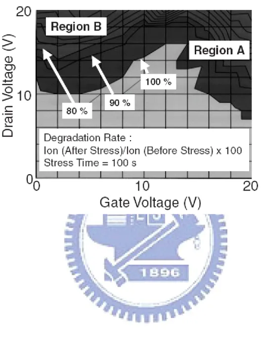
understanding of reliability mechanisms become more and more necessary. In LTPS TFTs, several DC stress degradation mechanisms have been reported. In 2002 Satoshi Inoue paper brought up the stress voltage dependence of the Vth shift in poly-Si TFTs, as shown in Figure
1-2. Thus, in 2003 Satoshi Inoue’s paper classified the degenerated
phenomena. Figure 1-3 shows the effect of stress voltage on the Ion
variation in TFTs. This result indicates two main degradation regions, the stress voltage of region A and region B. At first, hot carrier degradation is considered to originate from the damage of the metal-oxide-semiconductor (MOS) interface and of the channel poly-Si layer near the drain of TFTs. On the other hand, self-heating degradation is thought to originate in breaking of Si-H bonds and regeneration of dangling bonds in the MOS interface and channel poly-Si layers. In region A, the dominant degradation mechanism is self-heating, both the drain and gate voltages are high, typically over 10V. In region B, the dominant degradation mechanism is hot carrier, only the stress drain voltage is high, typically over 10V, and gate voltage is low, typically from 2V to 5V.
1.4 Organization of this thesis
This thesis is organized as followed: in Chapter 2, introduction of poly-Si crystallization methods and fabrication process of poly-Si TFTs on metal foil substrate. Simultaneously, the instruments for bending system and current-voltage (I-V) measurement will be introduced. Then we describe the methods of device parameter extraction. In Chapter 3,
the experiment processes and conditions will be illustrated. The content includes the current-voltage (I-V) measurement under bending/ flat condition and use X-ray diffraction measurement (XRD) to measure grain boundary orientation and material characteristics. Then we study the reliability of p-channel polycrystalline silicon (poly-Si) thin film transistors (TFTs) on steel foil substrates under drain bias instability stress. We use strain molds which are different form tensile (outward, Rp) and compressive (inward, Rn) [see Fig1.1]. There have radius of curvature (R) from 50 millimeter to 10 millimeter in our bending molds.
Then in Chapter 4, we try to explain the results of our experiment. After bending several times and then flattens, the threshold voltage (Vth) shift and sub threshold swim (S.S) degradation, but after hundreds of times bending the current-voltage properties would be stable. Then we discuss the electronic properties’ variation under strain condition. Under compressive condition the hole mobility is better than flat and in flat condition the hole mobility is better than tensile condition. And we also find out threshold voltage shift and threshold slope degradation no matter what kind of bending status. At last we utilize the DC drain bias stress the elements under bending condition. Although the on current and sub threshold swim degradation, we find out electronic properties under compressive status after stress is better than plan and tensile status. In order to explain the phenomenon, used amorphous silicon and MOS TFTs mechanism to accounts of our experiments is necessary. Finally in
Chapter 5, we conclude our results and integrate my thesis. And put my
Chapter 2 Fabrication and Characterization:
2.1 Fabrication process of poly-Si on metal foil
In this research, our TFT process developed for the LCD
active-matrix backplanes is a low temperature poly-silicon process (LTPS). The TFTs were fabricated on a SS304 stainless steel foil (thickness=70µm, area=10cm×10cm) by conventional LTPS process, where a-Si is crystallized using a XeCl excimer laser. All of the fabrication of poly-Si on metal foil, we different this part of process flow paths for four parts as follow:
2.1.1 Metal polishing
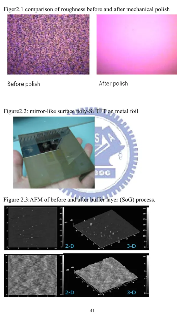
After degreasing and cleaning, metal foils are polished by mechanical polishing process [2.1], which provides a drastic reduction of roughness. Propose of mechanical polishing process is flatten our substrate less than 2 nm. Average roughness (Ra) was reduced from 95 nm before polishing down to 0.75 nm [Fig 2.1] after polishing which gives finally mirror-like surface [Fig 2.2].
2.1.2 Thick insulator
After that, the buffer layer was coated on the polished steel foil in order to obtain a smooth and pinhole free surface. This insulator can be inorganic, such as PECVD SiNx, but organic materials such as spin coated polymer are also being evaluated. This buffer layer should exhibit
high adhesion to the flexible metal. The buffer layer not only reduced the surface roughness of steel foil but also prevented contamination from steel substrate during the heating processes that a smoother steel foil surface was critical in TFTs process and could improve the TFT alignment in photolithography process. So we spin coating silicon on glass 2um as buffer layer in order to reduce the pin hole and roughness. See this Figure 2.3 of AFM, before buffer layer process the roughness is about 0.891nm and after buffer layer process the roughness is about 0.499nm. Then we deposited SiNx 3000A as smooth layer. After fabrication of the inorganic SiNx layers, TFT were islanded to release the stress. Therefore, the substrate was flat, indicating no global stress. So PECVD SiNx was preferred to polymer and chosen as insulator layer for the present LTPS process on metal [Fig. 2.4(a)(b)].
2.1.3 LTPS process
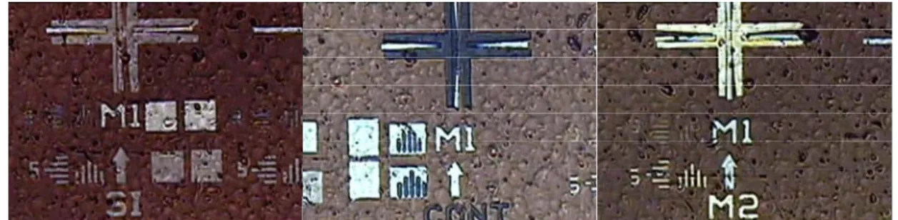
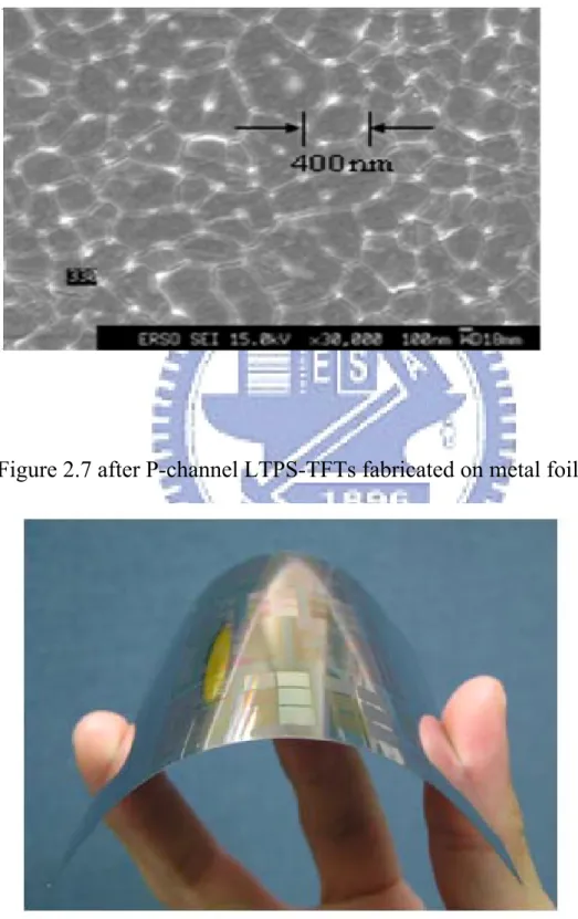
After pre-treatment of steel foils, it was glued onto glass for the subsequent LTPS-TFT processes. Figure 2.3 illustrates the conventional LTPS-TFT structure where M1 represents the gate metal and M2 represents the source and drain metal of TFT. The Cr is used as gate, source and drain metal as shown in [Fig. 2.5]. The maximum process temperature was 200°C in the CVD processes, including a-Si (50nm), gate oxide (100nm) and inter layer dielectric (ILD) oxide (300nm) deposition. The pulse excimer laser with 308nm wavelength was used to induce the poly-Si crystallization. The crystallized poly-silicon sample was etched by seco-etching solution, and scanning electron microscope
(SEM) was utilized to observe the surface image of poly-Si layer, as showed in [Fig. 2.6]. The grain size of poly Si showed in SEM about 0.4 micro meters. The electrical characteristics of p-type LTPS-TFTs were measured by HP4156 parametric analyzer. We used top gate, self-alignment polycrystalline Si TFT, adopting an organic layer as the first gate insulator on metal foil. The self-aligned ion doping technology was used to produce p-type LTPS TFT. The activation process was performed at 450 to reduce the resi℃ stance of P+ ion doping area by the rapid thermal process (RTP). At last we use SiNx 1000A as preservation layer and then anneal 2 hours to Hydrogenate by Atmospheric Anneal Furnace. The bus line metals are exposed to high stress during the plasma enhanced chemical vapor deposition (PECVD) process at 200°C because the CTE was mismatched between substrate and metal line. Therefore, the ductility of the bus line metal is important for the electronic device on metal foil substrate. [Fig. 2.7]
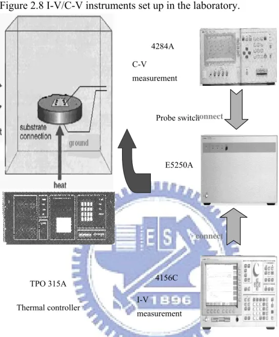
2.1.4 Introduction of Instruments for C-V Measurement
The electrical test setup of HP4156C semiconductor parameter analyzer is utilized in this experiment, illustrated in Figure 2.8, a probe station is situated inside a dark box. The ground probe station is furnished with an electrically isolated, water-cooled thermal chuck. The chuck is controlled by Temptronic TPO315A thermal controller, which can operate temperature from 25°C to 200°C. An Agilent 4156C precision semiconductor parameter analyzer can provide I-V measurement, bias for BTS, and quasi C-V measurement, etc. We employ the ICS (Interactive Characterization Software) to obtain the output and transfer
characteristics, like VD-ID, VG-ID (Linear), VG-ID (saturation), and extract
the typical semiconductor parameters.
In order to investigate the effect of the DC gate-bias stress under bending condition (i.e., the gate was given a constant voltage while the source and the drain were grounded) on the electrical parameters of excimer laser annealing (ELA) low temperature poly-silicon TFTs, the p-type poly Si structure on metal foil setup is shown in Figure 2.7.
2.2 Methods of Device Parameter Extraction
In this section, we will introduce the methods of typical parameter extraction such as threshold voltage VT, subthreshold swing ( S.S),
field-effect mobility
µ
FE, flat band voltage VFB, trap density Nt , activateenergy Ea, parasitic series resistance Rpa, field-effect mobility without the
effect of series resistance
µ
FE0 and the strain of the surface εsurface.We willshow it as follow.
2.2.1 Determination of the Threshold Voltage (Vth)
Several methods are used determinate the threshold voltage (Vth), which is the most important parameter of semiconductor device. The method we determinate in this thesis is the constant drain current method, the voltage at a specific normalized drain current NID is taken as the
threshold voltage. This technology is easy to extract and adopted in most TFTs. It can give a threshold voltage close to that obtained by the complex linear extrapolation method. Typically, the specific normalized current NID = ID/(W/L) is defined at 10nA for VD operated in linear
region and 100nA for VD operated in saturation region in poly Si TFTs
devices, to extract the threshold voltage of TFTs in most papers.
2.2.2 Determination of the Subthreshold Swing (S.S)
Subthreshold swing (V/dec) is a significant parameter to describe the control ability of gate bias toward drain current and the efficiency of the switch turning on and off. It is defined as the amount of gate voltage required to increase/decrease drain current by one order of magnitude. It should be independent of drain voltage and gate voltage. However, in reality, the subthreshold swing might increase with drain voltage due to the short-channel effects such as charge sharing, avalanche multiplication, and punch through-like effects. It is also related to the gate voltage due to some undesirable factors such as serial resistance and interface state. It is defined as one-half of the gate voltage required to decrease the threshold current by two orders of magnitude. The formula can be shown that the expression for S.S is given by
) (log d g I V SS ∂ ∂ =
In general, many researchers use the way to evaluate S.S as follow:
S.S.= [Vg(NId=10nA)- Vg(NId=100pA)] / 2
The threshold current is specified to be the drain current when the gate voltage is equal to the threshold voltage [Fig2.9].
The field-effect mobility (
µ
FE) is determined from the transconductancegm at low drain voltage (linear region). The transfer characteristics of
poly-Si TFTs are similar to those of conventional MOSFETs, ignoring any other non-ideal effect and assuming the electric field in the channel is uniform, so the first order I-V relationship in the bulk Si MOSFETs can be applied to the poly-Si TFTs, which can be expressed as
2 1 [( ) ] 2 D FE ox G T D D W I C V V V V L µ = − − (2-1) Where Cox is the gate oxide capacitance per unit area
W is channel width L is channel length
VT is the threshold voltage.
If VD is much smaller than (VG-VT) (i.e., VD << VG-VT ) and VG > VT, the
drain current can be approximated as:
( ) D FE ox G T D W I C V V V L µ = − (2-2) The transconductance is defined as
D FE ox const V G D m V L WC V I g D = µ ∂ ∂ = = . (2-3)
Therefore, the field-effect mobility can be obtained by
gm D ox FE WV C L = µ (2-4)
The mobility value was taken from Equation (2-4) with maximumµFE.
2.2.4 Determination of the trap density N
tmodel, we know there are the relationship with grain boundary potential barrier height VB and doping concentration ND. When doping
concentration ND [cm-3] increase more than Nt/L We can express the
grain boundary potential barrier height VB as follow equation:
2 2 2 2 8 t t B s s N qN qn V n n ε ε ⎛ ⎞ = ⎜ ⎟ = ⎝ ⎠
Where Nt[cm-2] is density of acceptor-like traps at grain boundary VB is the grain boundary potential barrier height
n [cm-3] is the carrier concentration
Based on this consideration, the amount of trap state density Nt can be
extracted from the current-voltage characteristics of poly-Si TFTs. As proposed by Levinson et al. [2.2], the I-V characteristics including the trap density can be obtained by the following equation
(
)
3(
2)
0 exp 8 t ch D ox G TH D s ox G TH q N t W I C V V V L kT C V V µ ε ⎛ ⎞ = − ⎜⎜− ⎟⎟ − ⎝ ⎠This equation had been further corrected by Proano et al. by considering the mobility under low gate bias [2.3]. It is found that the behavior of carrier mobility under low gate bias can be expressed more correctly by using the flat-band voltage VFB instead of the threshold voltage VTH.
Moreover, a better approximation for channel thickness tch in an undoped
material is given by defining the channel thickness as the thickness at which 80 percent of the total charge resides. Therefore, by solving the Poisson’s equation, the channel thickness is given by
(
)
8 s ox ch ox G FB kT t qC V V ε ε = − (2-7)The drain current of poly-Si TFTs then should be expressed as 2 2 0 ( ) exp 2( )2 ox t s D ox G FB D ox G FB q N W I C V V V L C V V ε ε µ ⎛ ⎞ ⎜ ⎟ ⎜ ⎟ = − − − ⎜ ⎟ ⎜ ⎟ ⎝ ⎠ (2-8)
The effective trap state density then can be obtained from the slope of the curve ln⎣⎡ID/
(
VG−VFB)
⎤⎦ versus(
)
2
G FB
V −V − as in Figure 2.10 and we can
calculate the slope from it. The grain boundary trap-state density can be determined from the square root of the slope directly, expressed by the simplified equation below.
ox trap C N Slope q = (2-9)
2.2.5 Determination of the parasitic series resistance R
pa:
In this section, we want to get the parasitic series resistance. Because there are resistances of any materials, in source/drain parts we called the resistance as parasitic series resistance (Rpa) and in channel part we called
the resistance as channel resistance (Rch). They can be extracted by
well-known transmission line method (TLM) [2.4-5] using a series of TFTs with different channel lengths measured at a low source/drain voltage, so we can neglect the space-charge-limited currents (SCLC) effect. The total TFT ON-resistance is as follow:
(2-10) Where rch is the channel length resistance per channel-length unit and
and (2-2), we can express the total ON-resistance RT as function of
µ
FEand threshold voltage:
(2.11)
The same equation applied to the ideal TFT lets us express the channel resistance as a function of the intrinsic mobility (
µ
FEi) and thresholdvoltage (VTi), which are representative of the conduction channel material,
without the influence of the TFT series resistance:
(2.12) The extraction of the TFT source and drain series resistance and intrinsic field-effect mobility and threshold voltage is rather straightforward using a series of TFTs with different channel lengths. So we use different L and RT to plot the total ON-resistance as a function of the TFT channel length for different gate voltage. Ensuring that the TFT is in accumulation layer, and then we fit the experimental data to linear curves. We show in
Figure2.11. In the cross-point of fitting linear curve, we can obtain 2RS/D
from the y-intercepts. And then we can express field- effect mobility without series resistance as follow [2.6-7]:
(2-13) Where µ is the carrier field-effect mobility with series resistance
µi is the carrier field-effect mobility without series resistance
Rp (RS/D) is the series resistance
2.2.6 Determination of the strain of the surface:
In order to define the strain percentage to our investigation, we must find out the respective Young’s modulus of steel foil (Ys) and substrates (Yf). In our cases, Young’s modulus of film and substrate for
both Yf and Ys are 200 GPa [2.8-10]. The strain of surface function is
given by:
(
)
(
η)(
η)
η η ε x x R d df s surface + + + + ⎟⎟ ⎠ ⎞ ⎜⎜ ⎝ ⎛ + = 1 1 2 1 2 2 (2-14)Where η=df/ds and x=Yf/Ys, here, df =0.8µm and ds=80µm. There is
compressive or tensile strain with radius R =∞, ±50, ±40, ±30 and ±10 mm. So after transforming with strain equation, we can get the equivalent strain quantity shown in Table 2.
2.3 Experimental Procedures of Flexible characterization of
P-type poly-Si on metal foil
2.3.1 Experiment of flexibility test for p-type poly-Si on metal foil:
After fabrication of p channel polycrystalline silicon TFTs on metal foil, we measure electronic property by semiconductor parameter analyzer 4156. It exhibits superior characteristics such as field-effect mobility of 92 cm2/Vs, a threshold voltage of -5.4 V, and an on/off current ratio of more than 107 and substhreshold slope of 0.82 V/dec
[Fig.2.12]. But how could we know if the electronic property be affected
after bending several times. So we must use the flexibility test first before bending experiment. The device picture is shown in Figure 2.2. The
length and width is 10 x 10cm. we inflict the tensile stress (outward) to 6 cm parallel source/drain channel and then flat. We repeat to have back and forth bending 1~100times to the condition of test and then flat to measure the electronic characteristic of ID-VG and ID-VD. Then we repeat to have back and forth bending 400times (500times bending) to test and then flat to measure the electronic characteristic of ID-VG and ID-VD. Last we repeat again to have back and forth bending 500times (total 1000times bending) and then flat to measure the electronic characteristic of ID-VG and ID-VD. The model is shown in
Figure2.13.besides outward flexibility test we also inflict inward bending
tests in another new device. The radius of flexible curvature is 20 millimeter and transform to surface strain is about 0.281%. Then we measure and take pictures by optic microscope Charge Coupled Device (CCD) shown in Figure2.14.
2.3.2 Experiment of electronic property variation under bending status:
In this part, we use models of bending radius of curvature (R) from 50 millimeter to 10 millimeter in our bending molds. That’s different into compressive and tensile two parts [Fig. 1.1]. [2.11]-[2.12]. After the test of flexible device stability, we make sure the electronic property stable. Then we start the experiment of electronic properties variation under bending status by these devices. The bending molds are shown in Figure 2.15 that the radius of curvature from 10 millimeter to 50 millimeter. We defined the bending direction shown in Figure
and biaxial strain. Because of different channel devices in the same substrates, the strain force is the same in different channel position or there exhibits two direction strain forces in three dimensional spaces; we call biaxial strain (global strain). There is different strain force in different channel position in the same device; this kind of strain is one dimensional strain force in three dimensional spaces which we called uniaxial strain (local strain). In our investigation the strain force is uniaxial strain and parallels the source/drain current channel. We measure the drain current virus gate voltage curve and drain current virus drain voltage curve under bending status by HP4156 parametric analyzer. In order to make sure of the increase of state in polycrystalline Si channel material under the inwardly and outwardly bent situation, the activation energy (Ea) of polycrystalline TFTs with different bending situation was
extracted from varied temperature measurement in the temperature range from room to 150oC.
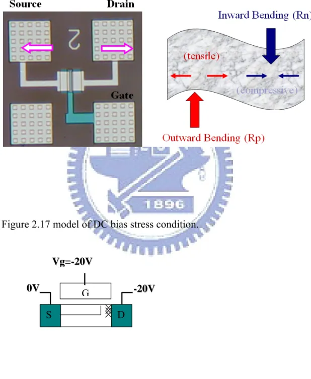
2.3.3 Experiment of DC bias stress under bending condition:
After measurement under bending status, we flat again and make sure the property return. Then we start the experiment of instability under bending condition. First, find out two different test keys but same length/width in one sample. Then measure the electronic property in one test key; supply -20 voltage drain bias stress and -20 voltage gate bias stresses as Figure 2.17 in order to see the self heating effect in 10, 100, 1000 and 2000 seconds. The TFT length/width is 30 over 10 micrometers. Second, we repeat the drain and gate bias stress measurement in another test key of the same sample under tensile status in 10, 100, 1000 and 2000
seconds and then flatten again to mature the electronic properties. Last we repeat the drain and gate bias stress measurement in the same length/width test key of another sample under compressive sample in10, 100, 1000 and 2000 seconds and flatten to mature the electronic properties again.
Chapter 3 Results and discussion:
3.1 Electrical Performance after Flexibility Test of P-type Poly-Si on Metal Foil
3.1.1 Electrical Performance after First-time and multi-times Flexibility Tests:
After the flexibility tests, we extracted the Gm maximum, mobility and threshold voltage to compare with the electronic properties after many times flexibility. It is shown in Table 2. We find out the mobility changes very small after 1, 10, 100,500 and 1000 flexibility tests. But threshold voltage shift during 100 times bending tests then become stable. In Figure 3.1(a)-(b), there are all serious threshold voltage shifts at first bending test about 0.2 voltage shifts. Then after first bending test, the property becomes stable little by little. Finally 500 times bending create 0.004 voltage shifts and we think it almost in error value ranges. There is more serious shift on inward bending test. But mobility is not change very much under inward or outward flexibility test. We transform rate of mobility change after 1000 times test; it is less than 0.9%. In this way we consider the mobility is very stable after 1000times inward and outward test.
For the results, we assume when we bend first times create mass broken bonds by bending strain. Because there is also density of states in poly silicon [Fig.3.2], deep states near mid-gap are associated with broken bonds and shallow tail states are associated with strained bonds. We consider the flexible action will account broken bonds increase at first 100 times. Then the weak bonds in deep states broken but other
strong bonds did not be effected so after 100 times tests the characteristics become stable. In order to verify our think, we try to extract the trap density.
3.1.2 Analysis of trap density Extraction:
In Figure3.3-4, we extracted the trap density clouding flat to 1000 times flexibility tests. The variation rate of trap density from first 100 times tests is about 5.357% and last 900 times tests is about 0.068% of inward test. And variation rate of trap density from first 100 times tests is about 5.31% and last 900 times tests is about 0.084% of outward test. So this results show no mater outward or inward bending will account broken bonds increase after first 100 times bending tests. And inward test create more damage than outward test. We assume compressive strain cause more serious damage than tensile strain in our case. Then we believe the device characteristic become stable step by step.
3.2 Electrical Performance under Different Mechanical Strain 3.2.1 Electrical Property Variation under Different Bending Status:
Before the mechanical stress applied, we make sure the device property already pass flexibility test and characteristic becomes stable. In this way we can use mechanical bending molds to bend our sample several times and the device keeps the characteristics. The p-channel LTPS TFTs we measure before mechanical bending exhibited superior characteristics such as field-effect mobility of 92 cm2/Vs, a threshold voltage of -5.7 V, and an on/off current ratio higher than 107 and substhreshold slope of 0.85 V/dec. However, a slight increase of
subthreshold slope (SS) from 0.85(R= ∞) to 1.02 V/dec(Rn=-10mm) was
observed in the case of compressive stressing(the insert of Fig3.5(a)) while SS increased from 0.85(R= ∞) to 0.97 V/dec(Rp=10mm) with the
increase of tensile strain, shown in Fig3.5(b). It also was observed that the threshold voltage of poly-Si TFT devices, applied at VD= -10 V,
increased as a function of either compressive or tensile strain with radius R= ∞, ±50, ±40, ±30 and ±10 mm. We enlarge the I-V curve on the upper right corner of the figures. Then transformed the strain of the surface
[Table3], we draw the threshold voltage virus strain percentage in Figure 3.6. The creation of the dangling bonds in the polycrystalline silicon is
mainly due to the breakage of weak Si-Si bonds during mechanical strain measurements [Fig3.2]. The bond strength can be affected by the strain and thus the creation of dangling bonds will depend on the curvature
[3.1-2]. Therefore, this could cause the enlargement of threshold voltage
with increasing mechanical strains. The compressive strain (inward) create more dangling bonds in the polycrystalline silicon than tensile strain; the results agree with the flexibility tests which showed inward test threshold voltage shift more serious than outward test. Figure 3.7 shows the normalized mobility virus strain percentage. An abnormal results that mobility increase under compressive bending condition but decrease under tensile bending condition. For this normalized results, we try to analyze activation energy and trap density to find out the reason.
3.2.2 Analysis of Activation Energy and trap density Extraction:
We utilize varied temperature measurement in the temperature range from room to 120 to ℃ extract the activation energy (Ea) of
polycrystalline TFTs with different bending situation showing as follow
Figure3.8 [3.3]. The energy barrier of tensile is higher than flat curve,
and compressive curve is lowest. So there is the lowest energy barrier in compressive curve. This result matches our experiment. For more intimate investigation, we try to find many kinds of models in poly crystalline silicon strain effect. We extracted the trap density under different bending condition to investigate the trap density variation in
Figure 3.9 (a)-(b). Then we calculate the trap density variation rate. In
0.08% strain(R=50mm), the variation rate is about 0.9% in tensile status but in 0.1347% strain(R=30mm) it is about 2.68 % until 0.404% strain(R=10mm) means after 0.1347% strain the trap increase slightly. The same phenomenon appeared in compressive status, in 0.08% strain, the variation rate is about 1.15 % in tensile status but in 0.1347% strain it is about 4.21 % until 0.404% strain. Once we mature in bending status no matter what compressive or tensile condition, the trap densities increase. So we explain the bending action measurement would act trap densities and under compressive status more serious. But generally the electric characteristic is still very will. But in the other way, we don’t know which mechanisms affected the drain current variation, so it is necessary to clarify our results step by step. One of conditions is the effect of parasitic series resistance.
3.2.3 Analysis of Parasitical Series Resistance Extraction:
To make sure if parasitic series resistance affects the mobility under bending status. The way we use is to measure the different channel length I-V curve on another device under flat, compressive and tensile
status. And then extracted the parasitic series resistance and field effected mobility except parasitic series resistance to discuss the difference of mobility. The channel length we measure from 2 to 50 micro meters and width length 10 micro meters and strain percentage from -4.04% (Rn=10mm) to 4.04% (Rp=10mm). The figure 3.10(a)-(b) illustration of the transmission line methods used to extract the S/D series resistance. The total ON resistance Rm*W has been plotted as a function of the TFT
channel length for different gate voltage. The cross-point equal two times of Rpa is about 7.7 kΩ. So Rpa in flat status is about 3.85 kΩ. Different
radiuses of curvatures have different Rpa [Fig 3.11]. We extracted five
times and calculate arithmetic mean in our error bar. In figure 3.11 the parasitical series resistances are almost straight in different bending status. After calculation of every bending status, we draw the normalized mobility except parasitic series resistance virus strain percentage in
Figure 3.12 [3.4] and we also draw different channel length normalized
mobility except parasitic series resistance virus strain percentage to see the integral trends [Fig 3.13]. In these two figures we can see even except parasitic series resistance the compressive condition still has high mobility than flat and tensile condition has lowest mobility from channel length 2 to 50 micro meters. So we can find out the mobility still affected by strain percentage even the mobility already rejected parasitic series resistance effects. This means parasitic series resistance is not the main reason affected mobility change. Even under different strain percentage the series resistance change very little and we think this is not for mobility increase reason under compressive condition. So we try to find other possibility to explain our results. These characteristics are similar to
those in the single crystalline metal oxide semiconductor devices, due to the strain-induced band splitting effects [3.5].
3.2.3-1 Factor affects single crystalline Si mobility:
We utilize p-channel metal oxide semiconductor devices strain mechanism [3.5-6] to explain our results. Recently many researches for biaxial (uniaxial) strain effects of p-channel and n-channel MOSFET improve the drain current [3.6-10]. The table 4 arranges the biaxial (uniaxial) strain effects to PMOS and NMOS drain current. We can find out biaxial tensile strain could improve PMOS and NMOS drain current simultaneously, but uniaxial strain effects improve one device instead of depraving another device [example: tensile (compressive) modify NMOS (PMOS) but deprave PMOS (NMOS)]. These devices characteristics attribute to changing of mobility in drain current equation by strain effects. If it examine carrier mobility change by band structure related parameter, the carrier distributed rate in valley band、scattering rate and effect mass are the most direct reasons of these three parameters. There are three factors affect single crystalline silicon mobility: silicon thickness、surface orientation and strain. First, all of our samples have the same silicon thickness about 500Å so this factor is constant. Second, the surface orientation relationship graph is in figure 3.14[3.10-11] and because our samples under the same crop of TFT devices, so the surface orientation are the same. In PMOS device, there is the highest hole mobility in (110) direction parallel the source/drain current path because of carrier repopulation [3.11]. It also indicates that (110) surface
orientation provides the higher drain current in compressive status than flat status. Because our samples are poly silicon TFT device, there is not only one surface orientation in our samples. The strain direction is dependant of mobility of gain for (110). In (110) surface for example, mobility of gain is overwhelmingly larger than those in the other channel direction. When the bending direction parallel the surface orientation (110), the tensile condition get low mobility of gain and compressive condition get higher mobility of gain. In our case, we must know the surface orientation so we sand a material sample to take XRD measurement. We use X-ray diffract meter (XRD) to analyze our sample surface structure in figure 3.15 (a)-(b). In order to make sure the XRD pulse of poly film is not affected by substrate material, we scan x-ray diffraction in positive and negative way simultaneously. We analyze the structure in Figure3.16 (a)-(b). The pulse FeCr0.29Ni0.16C0.06 is also existed in both positive and negative. We indicated that is our substrate material pulse. So off with FeCr0.29Ni0.16C0.06 pulse, we can indicate (111) (110) (100) in our poly silicon samples. (4,0,0) pulse is the same orientation with (1,0,0) but in other views, so (2,2,0) pulse is the same orientation with (1,1,0) but in other views and (2,2,2) pulse is the same orientation with (1,1,0) but in other views. We know as long as it exhibited (1,1,0) pulse, we can get higher drain current in compressive condition and worse drain current in tensile condition.
3.2.3-2 Single crystalline strain effect:
Figure 3.17 showed that silicon structure conduction band and
(biaxial) tensile and compressive strain. These characteristics are similar to our poly silicon device on metal foil! Before strain effect, the six valley bands of silicon conduction band energy degenerated, and heavy hole (HH) and light hole (LH) of valence bands are also energy degenerated. When biaxial tensile strain inflicted, the in-of-plane lattices are stretched and out-of-plane lattices compressed [3.5] [3.13]. It corresponded kx and ky direction fourfold degenerate (∆4) energy band upgrade and kz direction twofold degenerate (∆2) energy band downgrade. So most electrons distributed in twofold degenerate (∆2) energy band because of lower energy band, the effect mass decrease. Besides this, the biaxial strain leaded to strain-induced band splitting then another way degrade inter-valley scattering rate and effect density of states of conduction band. In this way lower effect mass and inter-valley lower scattering rate leaded to electron mobility increase and improved drain current. The same reason as uni-axial strain, figure 3.18 [3.11] uppers are schematic illustrations of strain induced carrier repopulation among six valleys in silicon conduction band. Applied strains are uni-axial tensile and uni-axial compressive strain along <110> which is Si single crystal surface orientations. The change of six valleys in silicon conduction band is dependent on surface orientation, strain and silicon thickness as the above-mentioned [3.11]. Because all of our devices are follow one thickness of silicon layer, 50 nanometers, so the susceptible factors of six valleys in silicon conduction band are surface orientation and strain.
Figure 3.19 showed the surface orientation and current flow directions.
The in-plane channel direction (θ) is defined as an angle between the channel and the notch orientation. The bottoms are schematic
representations of the qui-energy lines of conduction band and valence band [3.14] [3.15] for each surface. So we can know the qui-energy lines of conduction band and valence band are different in different surface orientation. In our case, the effected factors of uniaxial tensile and compressive strain:
1. Cause of light hole and heavy hole separation then reduce scattering effect, so τ(mean free time) increase.
2. Cause of apparent band warping, then hole effect mass reduce (Mn).
Because mobility is equal electron quantity multiply mean free time over hole effect mass, so uniaxial compressive could increase µ.
3.3 Reliability Analysis of poly-Si TFT under Bending Condition 3.3.1 Gate DC Bias Stress Reliability Investigations:
In this section, we use three the same length/width (10/30micro meters) but different test keys to measure the I-V curve. First one we stress 10 seconds to 2000 seconds DC bias stress in flat status in Figure 3.20 as comparison. There are obvious on current degrade after 1000 seconds stress. After 2000 seconds stress, the threshold voltage shift about 0.17 volt and mobility variation rate is about 49.4% but S.S degraded unobvious. Then we measure another two test keys for DC drain bias stress from 10 to 2000 seconds under compressive (Rn=10) and tensile (Rp=10) status [Fig 3.21 (a)-(b)]. There are also on current degradation after 1000 seconds DC stress and obvious S.S degradation. In order to compare with the stress effect under different bending status, we draw the threshold voltage shift and normalized mobility virus strain
percentages in figure 3.22-3.23. In these figures, threshold voltage and mobility decrease slightly after 1000 seconds DC bias stress but they are still decrease seriously after 1000 seconds DC bias stress in bending status.
3.3.2 Comparison of Electrical Property under Different Condition
There is superior characteristic in compressive status than tensile status after stress, and more than this, we calculate mobility variation rate comparison before and after stress in figure 3.24. Under three different status, there are still damaged after 1000 seconds in bending status. After 2000 seconds stress, compressive status has better characteristics than flat status and the worst is under tensile status. We explain the mobility affected by strain so silicon six valley bands separated and band warping in compressive condition. In bending status there are electron accumulations in silicon lattice surface so the mobility decreased slowly. But after 1000 seconds the accumulated electrons affected so the mobility continued degradation. Because of six valley bands warping, the DC bias stress damaged slightly than flat status. And there is the worst mobility performance because of light hole and heavy hole keep near to each other in tensile condition. There is more than one effect exhibit in the DC bias stress experiments.
Chapter 4 Conclusions and Future Work:
4.1 Conclusion:
In this thesis, we fabricated P- channel polycrystalline thin film transistors on metal foil and it exhibited superior characteristics such as a field-effect mobility of 92.45 cm2/Vs, a threshold voltage of -5.7V, the subthreshold slope of 0.85V/dec at VD=-10V, the Ion/Ioff ratio greater than
107. Then we make these samples in flexibility tests in order to conform if
flexible action influences the electric property. We find out first 100 times bending tests make most serious damages and trap densities then become stable step by step. After this, we measured the electric properties under different radius of curvature bending status and fund out the threshold voltage degraded following the strain percentage. And it has greater mobility in compressive condition than flat and tensile conditions. After extracted parasitical resistances and activation energy and trap densities, we assumed this effect is because of silicon lattices warping and light hole and heavy hole separated so the effect field mobility changed. Last in DC drain bias stress under bending status, threshold voltage shift and on current degraded slightly after 1000 seconds stress in flat condition but it still damaged silicon lattices even after 1000 seconds under bending status. But no matter stress or flexibility tests or mechanical bending measurement, inward (compressive) status has serious internal damage than outward (tensile) and greater mobility performance. We believe these researches will improve the development of poly TFTs on metal foil technology. E-book and e-labels and flexible signage industry may become practical.
4.2 Future work:
After these researches, we will investigate poly-Si TFT AC bias stress under bending status to discuss protracted alternating current influence. For life’s application, we will sustain to research poly-Si TFT stress in sun’s rays under bending status and compared with our results. Last for electric labels application, we will research with small size poly-TFT on metal foil under sun’s ray’s illumination.
Reference:
Chapter1:
[1.1] A. T. Voutsas, IEEE Trans. Electron Devices 50, 1494 _2003_.
[1.2] P. Migliorato, C. Reita, G. Tallarida, M. Quinn and G. Fortunato,
“Anomalous Off-Current Mechanisms in N-Channel Poly-Si Thin Film Transistors.” Solid-State-Electronics, Vol. 38, No. 12, pp.2075-2079, 1995.
[1.3] M. Hack, I-W. Wu, T. J. King and A. G. Lewis, “Analysis of
Leakage Currents in Poly-silicon Thin Film Transistors,” IEDM Tech. Dig., Vol. 93, pp. 385-388, December 1993.
[1.4] K. Ono, T. Aoyama, N. Konishi, and K. Miyata, “Analysis of
Current-Voltage Characteristics of Low-Temperature-Processed Polysilicon Thin-Film Transistors,” IEEE Trans. Electron Devices, Vol. 39, No. 4, pp. 792-802, April 1992.
[1.5] A. Rodriguez, E. G. Moreno, H. Pattyn, J. F. Nijs, and R. P.
Mertens, “Model for the Anomalous Off-Current of Polysilicon Thin-Film Transistors and Diodes” IEEE Trans. Electron Devices, Vol. 40, No. 5, pp.938-943, May 1993.
[1.6] K. Y. Choi and M. K. Han, “A Novel Gate-Overlapped LDD
Poly-Si Thin-Film Transistor,” IEEE Electron Device Lett., Vol. 17, No. 12, pp. 566-568, December 1996.
[1.7] T. I. Kamins and Marcoux, “Hydrogenation of Transistors
Fabricated in Polycrystalline-Silicon Films,” IEEE Electron Devices Lett., Vol. EDL-1, No. 8, pp. 159-161, August 1980.
[1.8] B. A. Khan and R. Pandya, “Activation Energy of Source-Drain
Current in Hydrogenated and Unhydrogenated Polysilicon Thin-Film Transistors,” IEEE Trans. Electron Devices, Vol. 37, No. 7, pp.1727-1734, July 1990.
[1.9] K. Baert, H. Murai, K. Kobayashi, H. Namizaki, and M. Nunoshita,
“Hydrogen Passivation of Polysilicon Thin-Film Transistors by Electron-Cyclotron-Resonance Plasma,” Jpn. J. Appl. Phys., Vol. 32, No. 6A, pp. 2601-2606, June 1993.
[1.10] S. D. Theiss and S. Wagner, IEEE Electron Device Lett. 17, 264
(1996)
[1.12] Y. Chen, J. Au, P. Kazlas, A. Ritenour, H. Gates and J. Goodman,
The Int. Electron Devices Meet. 2002, 389.
[1.13] E. Y. Ma, S. D. Theiss. M. H. Lu, C. C. Wu, J. C. Sturm and S.
Wagner, The Int. Electron Devices Meet. 1997, 535.
[1.14] T. Serikawa, and F. Omata , IEEE Electron Device Lett., 20, 574
(1999)
[1.15] M. Wu, X. Z. Bo, J. C. Sturm and S. Wagner, IEEE Trans. Electron
Devices 49, 1993 (2002).
[1.16] T. Afentakis, M. K. Hatalis, A. T. Voutsas and J. W. Hartzell,
Mater. Res. Soc. Symp. Proc. 769, H2.5.1 (2003).
[1.17] M. J. Powell, Appl. Phys. Lett., 43, 597 _1983_.
[1.18] A. R. Hepbum, J. M. Marshall, C. Main, M. J. Powell, and C. van
Berkel, Phys.Rev. Lett., 56, 2215 _1986_.
[1.19] H. Gleskova, S. Wagner, W. Soboyejo, and Z. Suo, J. Appl. Phys.
92, 6224 _2002_.
[1.20] S. H. Won, J. K. Chung, C. B. Lee, H. C. Nam, J. H. Hur, and J.
Jang, J. Electrochem. Soc. 151, G167 _2004_.
[1.21] François Templier , Bernard Aventurier, Patrick Demars,
Jean-Louis Botrel, Patrick Martin. Thin Solid Films 515 (2007) 7428–7432
[1.22] S. H. Won, J. K. Chung, C. B. Lee, H. C. Nam, J. H. Hur, and J.
Chapter2:
[2.1] S. Grego, J. Lewis, E. Vick and D. Temple, Thin Solid Film, 151,
4745(2007)
[2.2] P. Migliorato, C. Reita, G. Tallarida, M. Quinn and G. Fortunato,
“Anomalous Off-Current Mechanisms in N-Channel Poly-Si Thin Film Transistors.” Solid-State-Electronics, Vol. 38, No. 12, pp.2075-2079, 1995.
[2.3] R. E. Proano, R. S. Misage, D. G. Ast, “Development and Electrical
Properties of Undoped Polycrystalline Silicon Thin-Film Transistors,” IEEE Electron Device Lett. Vol. 36. No. 9. pp. 1915-1922, Sept. 1989.
[2.4] C. J. Drury, C. M. J. Mutsaers, C. M. Hart, M. Matters, and D.M. d.
Leeuw. Lowcost all polymer integrated circuits. Appl Phys Lett 73:108-110,1998
[2.5] G. H. Gelinck, T. C. T. Geuns, and D. M. d. Leeuw.
High-performance all-polymer integrated circuits. Appl Phys Lett 77:1487-1489,2000
[2.6] K. Y. Chan, E. Bunte, H. Stiebig, and D. Knipp, Materials Research
Society
Symposia Proceedings _Materials Research Society, Pittsburgh, 2007_, Vol. 989, p. 0989-A11-03.
[2.7] Y. -J. Yang, W. S. Ho, C.-F. Huang, S. T. Chang and C.W. Liu,
Appl. Phys. Lett. 91, 102103(2007).
[2.8]F. Templier, B. Aventurier, P. Demars, J.L. Botrel and P. Martin,
Thin Solid Film, 515, 7428(2007)
[2.9] S. W. Won, J. K Cheng, C. B. Lee and Jin Jang, J. Electro. Soc. 151,
G167(2004).
[2.10] S.W. Won, C. B. Lee, J. H. Hur and J. Jang, J. Kor. Phys. Soc. 42,
S685(2003).
[2.11]H. Gleskova, S. Wagner, Appl. Phys. Lett. 75, 3011(1999).
[2.12] F. Templier, B. Aventurier, P. Demars, J.L. Botrel and P. Martin,
Chapter3:
[3.1] H. Gleskova, S. Wagner, W. Soboyejo and Z. Suo, J. Appl. Phys.,92,
6224(2002).
[3.2]Y. Kuo, Thin Film Transistors Materials and Processes Volume 1,
135(2004).
[3.3] H.-C. Linl, K.-L. YehM.-H. Lee, Y.-C. Sui, IEDM 04
[3.4] P. C. Kuo, J. R. Abbas and M. Hatalis, Appl. Phys. Lett. 91,
243507(2007).
[3.5] Y. J. Yang, W. S. Ho, C. F. Huang, S. T. Chang and C.W. Liu, Appl.
Phys. Lett. 91, 102103(2007).
[3.6] T. Komoda et al., IEDM Tech. Dig., 2004.
[3.7] S. E. Thompson et al., IEEE Trans. Electron Devices, v.51, p.1790,
2004.
[3.8] K. Rim et al., IEEE Trans. Electron Devices, v47, p.1406, 2000. [3.9] K. Rim et al., IEDM Tech. Dig., p.517,1995.
[3.10] T. Tezuka et al., IEDM Tech. Dig., p.946,2001. [3.11] H. Irie et al., IEDM Tech. Dig., p.225, 2004.
[3.12] F. M. Bufler et al., IEEE Trans. Electron Devices, v50, p.278,
2003.
[3.13] Z. Ren., P. M. Solomon, M. Yang, and K. Rim JAP V94, Number2,
2004
[3.14] M.V. Fischetti el 01.. JAP 94(2003)1079
[3.15] M. V. Fischettia., Z. Ren, P. M. Solomon, M. Yang, and K. Rim,
Table:
Table1: Comparion of different substrates characteristics
Metal Foil Plastic µ-Glass Glass
Substrate Ti SS304 Fe/Ni Al PES Eagle
2000TM Corning 1737 Tg (°C) 1668 >1300 N/A 660 225 725 666 CTE(ppm/°C) 8.6 17.3 1.7-2.0 23.5 55 3 3.76 Water Absorption 0 0 0 0 1.4 0 0 Density(g/cm3) 4.507 7.86 8.0 2.7 1.37 2.36 2.54 Weight g/cm2 0.04/0.024 0.03 0.18 Thickness(mm) 0.1 0.05/0.03 0.1 0.2 0.2 0.1 0.7 Cost (NTD/cm2) 0.27 (30*30) 0.33 (30*40) 5 (10*10) 0.458 (37*47)
Table2: the electric properties of inward and outward flexibility tests
10/50 Flat inward100 Inward500 Inward1000
Gm 5.2E-8 5.24E-8 5.236E-8 5.24E-8
Vth -7.435 -7.63 -7.701 -7.705
Mobility 123.4 123.3 123.22 123.3
10/30 flat outward100 outward500 outward1000
Gm 1.37E-7 1.366E-7 1.36E-7 1.358E-7
Vth -6.13 -6.32 6.327 6.33
Mobility 64.5 64.31 64.01 63.93
Table3: transform from radius of curvature to surface strain percentage
R (mm) Strain (%) 10 0.404 20 0.35 30 0.1347 40 0.101 50 0.0808 flat 0 50 -0.0808 40 -0.101 30 -0.1347 20 -0.35 10 -0.404
Table 4: the relationship between biaxial (uniaxial) strain and NMOS (PMOS) drain current
Figures:
Figure1.1 illustration of mechanical bending measurement
Figer2.1 comparison of roughness before and after mechanical polish
Figure2.2: mirror-like surface poly-Si TFT on metal foil
Figure 2.4
(a)No SiNx on buffer layer as flatten layer. There are many particles and defects.
(b)Have SiNx as buffer layer.
Figure 2.5 the illustration of poly silicon TFT on metal foil

![Figure 2.10 Plotting of ( )lnDGFBIVV⎛ ⎞⎜⎟⎜−⎟ ⎝ ⎠ versus ( ) 2FBVG−V− . Temperature=125 O C Stress Bias V G = -30V W / L = 6 / 6 1/(V GS -V FB ) 2 (V -2 ) 0.004 0.005 0.006 0.007 0.008 0.009 0.010 0.011ln[IDS/(VGS-VFB)]-17.4-17.2-17.0-16.8-16.6-16.4-1](https://thumb-ap.123doks.com/thumbv2/9libinfo/8142631.166734/57.892.136.733.119.1155/figure-plotting-lndgfbivv-versus-fbvg-temperature-stress-bias.webp)


![TraditionalMLCalgorithmsmainlytacklethebatchMLCproblem,wheretheinputdataarepresentedinabatch[24,28].Nevertheless,inmanyMLCapplicationssuchase-mailcategorization[22],multi-labelexamplesarriveasastream.Onlineanalysisistherefore dimensionreducermotivatedbyma](data:image/gif;base64,R0lGODlhAQABAIAAAP///wAAACH5BAEAAAAALAAAAAABAAEAAAICRAEAOw==)