國
立
交
通
大
學
電信工程學系碩士班
碩
士
論
文
低功率 3.1 ~ 15 GHz 超寬頻混波器
Low-power Ultra-Wideband Mixer for 3.1 ~ 15GHz
研 究 生:陳秋榜
指導教授:周復芳 教授
低功率 3.1 ~ 15 GHz 超寬頻混波器
Low-power Ultra-Wideband Mixer for 3.1 ~ 15GHz
研 究 生:陳秋榜 Student:Chu-Bung Chen
指導教授:周復芳 Advisor:Dr. Christina Jou
國 立 交 通 大 學
電信工程學系碩士班
碩 士 論 文
A Thesis
Submitted to Department of Communication Engineering
College of Electrical and Computer Engineering
National Chiao Tung University
In Partial Fulfillment of the Requirements
For the Degree of
Master of Science
In
Communication Engineering
June 2006
Hsinchu, Taiwan, Republic of China
低功率 3.1 ~ 15 GHz 超寬頻混波器
研究生:陳秋榜 指導教授:周復芳 博士
國立交通大學電信工程學系碩士班
中文摘要
本論文主要是在研究低功率超寬頻混波器的設計,頻段則是設計在 3.1~15GHz, 設計方法包含以下幾種步驟,(一)輸入匹配 (二)混頻器主架構的選取 (三) current injection 配合低功率的設計 (四)偏壓的選取 (五)訊號走線的寄生效應 (六)Switch stage 對雜訊與增益的影響。在設計的過程中遇到了許多的問題,特別是 在架構的選取會影響直流偏移的問題,進而影響輸出訊號及準位等等,論文中會解釋 如何克服這些問題。電路設計在頻帶 3.1GHz ~ 15GHz,而基頻頻率則是設計在 10MHz 時,在量測的結果為電壓轉換增益約-0.7 ~ 6.1 左右、射頻輸入返回損耗為-10dB 以 下、切換級輸入返回損耗為-14dB 以下、P1dB 分布在-15 ~ -13dBm 內在頻帶 4GHz ~ 10GHz、以及 1 ~ 3 dBm 的 IIP3 在頻帶 4GHz ~ 10GHz,且此電路設計電路功率僅消耗 17.5mW,本電路使用台積電 0.18um CMOS 製程設計,並且在國家晶片系統設計中心量 測,其模擬設計與量測結果的差異在論文中做一些說明和討論。
Low-power Ultra-Wideband Mixer for 3.1 ~ 15GHz
Student:Chu-Bung Chen Advisor:Dr. Christina Jou
Department of Communication engineering
College of Electrical and Computer Engineering
National Chiao Tung University
Abstract
The topic of this thesis is to research the design of the low-power ultra-wideband mixer. The bandwidth is designed from 3.1GHz to 15 GHz. The design procedures include: (1) input matching networks (2) choice of architecture (3) current injection matches for the design of low power (4) choice of the bias point (5) parasitic effect of the signal’s routes (6) influence of noise figure and conversion gain with switch stage. When designing the ultra-wideband mixer, many problems are found. Especially, the DC Offset will be influenced by the architecture. And then the DC and signal of the output will be influenced, etc. The design procedures will explain how to conquer these problems in detail. This circuit is designed from 3.1 to 15 GHz. And IF is at 10MHz. The measurement results include: Conversion voltage gain is about -0.7 ~ 6.1 dB. RF input return loss is better than 10dB. The return loss of switching stage is better than 14dB. P1dB is about -15 ~ -13dBm from 4GHz to 10GHz. IIP3 is about 1 ~ 3dBm from 4GHz to 10GHz. Power consumption of the circuit is only 17.5mW. This circuit is fabricated in TSMC 0.18um CMOS. The circuit is measured at CIC. There are some discussion and statement about difference between simulation and measurement in this thesis.
誌謝
首先,我要感謝我的指導教授周復芳老師願意收我為研究生,讓我有機會在 919 實驗室學習,進入實驗室的這兩年來,在射頻電路領域中,從懵懂無知到小有心得, 這都要感謝老師的指導,並且提供一個良好的環境,讓我們能夠順利的完成研究。以 及國華學長給予我們協助,讓我們能夠更快速進入射頻電路的世界中,也感謝郭建男 教授及邱煥凱教授,讓我對電路設計與量測有更深入的了解。 接著要感謝在 919 實驗室陪我一起打拼的同學,唐兄、小明、博揚、小砲及小賴, 感謝你們的包容及鼓勵,讓我在生活和研究中克服了許許多多的問題,特別是碩一下 學期,每兩個禮拜大家就要一起趕作業,即使平時有在做作業,到了交作業的前一天, 大家還是要一起熬夜看日出的情景,仍然讓我印象深刻。已畢業的偉誠、家良、柏達、 欽賢、政宏及俊賢學長,在我們有困難的時候提供我們寶貴的經驗,也常常撥控回來 為我們學弟加油打氣。碩一的宇清、宜星、智鵬、瑞嫻、子豪、寶明及博班的匯儀學 長,感謝你們分擔了我在研究之餘所無法空出時間處理的瑣事,並且時常有逗趣的搞 笑,來放鬆我們緊繃的神經,還有專題生小郭和 sammy,感謝你們在我閒暇之餘陪我 到健身房鍛鍊身體,讓我有充沛的體力來做研究,感謝你們在碩士生涯的陪伴,因為 你們讓我的碩士生涯過的多彩多姿,祝福你們在往後的日子裡都能順利的向你們的目 標前進,當然也祝福你們能夠順利畢業。 最後我要感謝我的父母及家人不斷的給我鼓勵與支持,並且提供一個良好的環 境,讓我能無後顧之憂的專心在研究及學業上。僅以此論文獻給所有關心我的人,希 望你們能感受到我由衷的謝意。 秋榜 2006 夏 新竹 風城C
ONTENTS
Chinese Abstract ………...…Ⅰ English Abstract ………...……….Ⅱ Acknowledgement ………..……. Ⅲ Contents ………Ⅳ List of Tables ……….………Ⅵ List of Figures ………...………ⅦChapter 1 INTRODUCTION... 1
1.1 Background and Motivations ... 1
1.2 Thesis Organization ... 4
Chapter 2 LOW POWER ULTRA-WIDEBAND MIXER FOR
3.1GHz ~ 15GHz... 5
2.1 Introduction ... 5
2.2 Architecture ... 6
2.3 Analysis of Ultra-Wideband Mixer ... 7
2.3.1 The suitable topology for Ultra-Wideband Mixer ... 7
2.3.2 The RF and LO matching networks ... 12
2.3.3 Conversion Gain ... 13 2.3.4 Effects of Nonlinearity ... 13 2.3.5 Noise... 15 2.3.6 Port Isolation ... 18 2.3.7 Design flow ... 18 2.3.8 Layout Consideration ... 20
2.4.1 Measurement Consideration ... 22
2.4.2 Measurement Results... 24
2.4.3 Comparison... 35
2.5 IF Frequency Response and Circuit Netlist... 36
Chapter 3 CONCLUSIONS AND FUTURE PROSPECTS... 41
3.1 Conclusions ... 41
3.2 Future Prospects ... 42
List of Tables
Table 1 Summary Requirements of IEEE 802.15.3A... 2
Table 2 Stability Simulation – (1)... 19
Table 3 Stability Simulation – (2)... 20
Table 4 Summaries of Performance ... 34
Table 5 Comparison of Ultra-Wideband Mixer ... 35
List of Figures
Figure 1-1 FCC UWB Mask for Communications ... 2
Figure 2-1 Architecture of MBOA Receiver... 5
Figure 2-2 Schematic of the Ultra-Wideband Mixer ... 6
Figure 2-3 Schematic of Mixer with Single-ended RF and LO Port ... 8
Figure 2-4 IF Output Signal RF@ 3.1GHz... 9
Figure 2-5 IF Output Signal RF@ 7GHz... 9
Figure 2-6 IF Output Signal RF@ 10.6GHz... 9
Figure 2-7 RF Return Loss... 10
Figure 2-8 IF Output Signal RF@ 3.1GHz... 10
Figure 2-9 IF Output Signal RF@ 7GHz... 11
Figure 2-10 IF Output Signal RF@ 10.6GHz... 11
Figure 2-11 RF Return Loss... 11
Figure 2-12 Matching Network (a) L-Shape (b) L-Shape with Resistance... 12
Figure 2-13 Mixer Linearity... 14
Figure 2-14 Noise Source of Direct Switch ... 16
Figure 2-15 Single-balanced mixer with switch noise modeled at gate. ... 17
Figure 2-16 LO to RF Isolation... 18
Figure 2-17 The layout of proposed low-power UWB mixer... 21
Figure 2-18 Die Photograph of UWB Mixer ... 22
Figure 2-19 PCB... 23
Figure 2-20 Practical PCB test board of UWB Mixer ... 23
Figure 2-21 Measurement setup for
(a) conversion gain (b) input return loss (c) two-tone IIP3 testing... 24
Figure 2-22 Measurement Environment (a) Probe Station (b) Spectrum
Analyzer ... 25
Figure 2-23 Conversion Power Gain ... 26
Figure 2-24 Conversion Power Gain with LO Power Sweeping... 26
Figure 2-25 Return Loss of RF Port... 27
Figure 2-26 Return Loss of LO Port ... 27
Figure 2-27 P1dB for RF@4g LO@3.99GHz ... 28
Figure 2-28 P1dB for RF@6g LO@5.99GHz ... 28
Figure 2-29 P1dB for RF@8g LO@7.99GHz ... 29
Figure 2-30 P1dB for RF@10g LO@9.99GHz ... 29
Figure 2-31 IIP3 for RF@4g LO@3.99GHz ... 30
Figure 2-32 IIP3 for RF@6g LO@5.99GHz ... 30
Figure 2-33 IIP3 for RF@8g LO@7.99GHz ... 31
Figure 2-34 IIP3 for RF@10g LO@9.99GHz ... 31
Figure 2-35 Measured IF Waveform (a) RF@ 4GHz (b) RF@ 5GHz ... 32
Figure 2-36 Measured IF Waveform (a) RF@ 6GHz (b) RF@ 7GHz ... 32
Figure 2-37 Measured IF Waveform (a) RF@ 8GHz (b) RF@ 9GHz ... 32
Figure 2-38 Measured IF Waveform (a) RF@ 10GHz (b) RF@ 11GHz ... 33
Figure 2-39 Measured IF Waveform (a) RF@ 12GHz (b) RF@ 13GHz ... 33
Figure 2-40 Measured IF Waveform (a) RF@ 14GHz (b) RF@ 15GHz ... 33
Figure 2-41 Conversion Voltage Gain... 34
Figure 2-42 The Element Values and Currents ... 37
Figure 2-43 Signal’s Amplitude at net56s and net78s for RF@3GHz... 37
Figure 2-44 Signal’s Phase at net56s and net78s for RF@3GHz ... 38
Figure 2-45 Signal’s Amplitude at net56s and net78s for RF@15GHz... 38
Chapter 1
I
NTRODUCTION
1.1
Background and Motivations
With the technology development in wireless application, the demands for RF systems have been increased. There are many kinds of communication systems invented such as 802.11a, 802.11b/g to 802.15.3A, etc. The ultra-wideband (UWB) radio is a relatively new wireless technology that has recently been approved by the FCC (Federal Communications Commission) for commercial applications. Its bandwidth is from 3.1GHz to 10.6GHz. When compared to the narrow band wireless communications, UWB technology has the promising ability to provide high data rate at low cost with relatively low power consumption. It is thus envisioned as the foundation for replacing almost every cable at home or in an office with a high-speed short-range wireless connection that features hundreds of megabits of data per second. UWB has many other advantages such as low interference, high security for short-range wireless communication [1]. There are two proposed methods for UWB system: DS-CDMA (Direct-Sequence Code Division Multiplexing Access) and MB-OFDM (Multi-Band Orthogonal Frequency Division Multiplexing). Each proposal has advantages itself. Impulse radio has better permeation. Multi-Band system isn’t afraid of interference or occupation, because it can change to another band among twelve bands. Because UWB has characters such as good permeation, effective transmission and low power, it is very suitable for the application about PC, CE and Mobile. In order to meet the demands of the modern short-range wireless communication system, UWB system is the best choice.
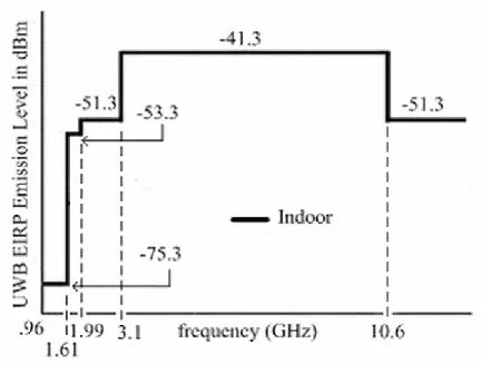
According to the regulation of FCC, the transmitted power is shown in Figure 1-1. It is limited not to exceed -41.25 dBm/MHz to prevent from interfering with the existing
communication systems. The transmitter may not need a power amplifier because of low transmit power. Therefore the architecture of transmitter can be reduced [2].
DS-CDMA and MB-OFDM proposals are applied for UWB. MB-OFDM is more supported than DS-CDMA, because MB-OFDM can gather the power of multi-path and has better efficient use of spectrum. In addition, the multi-band system can be suitable for the telecommunication regulations in many countries. Therefore the receiver for MB-OFDM is better proposal for UWB and has had great progress recently. The summary of specifications for MB-OFDM UWB system is shown in Table 1 [3]. The way to reduce the power consumption of the system is very important, while the performance must meet the specifications.
Figure 1-1 FCC UWB Mask for Communications Table 1 Summary Requirements of IEEE 802.15.3A
Parameter Value
Bit rate 110 , 200 , 480 Mbps
Range 30ft , 12ft
Power consumption 100mW , 250mW Bit error rate 1e-5
There are many researches and papers about ultra-wideband mixer begun and published in Taiwan, however their powers are usually in the range of 100~250 mW [4] [5][6]. It is too large to match the tendency of modern wireless communication. To avoid this drawback, a low power mixer of MB-OFDM UWB system is researched in this thesis.
1.2
Thesis Organization
Because this ultra-wideband mixer is designed for low power, the topology of mixer is very important. The double balanced mixer is the most common topology. It can reject the feedthrough both from RF and LO to IF port. However the single and differential ended LO inputs of double balance mixer have different characteristics. Each topology has advantages and drawbacks itself. Which topology is better for the low power design described in section 2.3.1.
After choosing the topology, the first thing is to design every part of the topology. ultra-wideband mixer comprises seven parts, including current mirror, current injection, transconductance stage, switching stage, load, and RF and LO input matching network. The basic principle of mixer and the methods to design for ultra-wideband mixer are shown from section 2.3.2 to 2.3.7.
From pre-simulation to post-simulation, there is a very important problem. Because the operation frequency band is from 3.1 to 15GHz, the parasitic effect is obvious. Therefore the performances of the pre-simulation won’t be matched for ones in post-simulation. The topology will determine the routes of RF signal, therefore the parasitic effect can be predicted. The skill of layout is very important to reduce the effect of parasitic. It is shown the layout to explain how the parasitic effect affects performance in section 2.3.8.
In section 2.4, the measurement results and comparing the performances among pre-simulation, post-simulation and other papers are discussed.
In section 2.5, the IF frequency response and the phase and amplitude of signal at some nodes in the circuit are discussed.
Chapter 2
L
OW
P
OWER
U
LTRA-
W
IDEBAND
M
IXER
F
OR
3.1GHz ~ 15GHz
2.1
Introduction
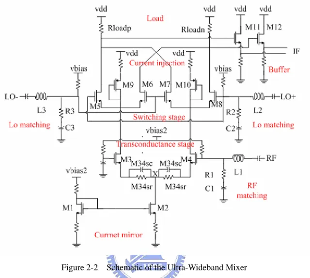
A low power RF device becomes a tendency as applied in the portable wireless communication systems. However, the performance including linearity and conversion gain will be degraded when we reduce the power or the supply voltage of RF mixer circuit. Hence, the implementation of the mixer with low power consumption, high linearity and high conversion gain would be a challenge in the RF front-end circuit. Figure 2-1 shows the architecture of MB-OFDM receiver [7]. The mixer of this receiver will be introduced in this thesis. Because the UWB is emphasized low power for short range wireless communication, how to reduce the power consumption, cost of circuit and have better performances are very important. Therefore the low power UWB mixer is designed shown in Figure 2-2.
Figure 2-2 Schematic of the Ultra-Wideband Mixer
Although there are many topologies of mixer designed for UWB. When the mixer is applied for low power and low voltage, the circuit will be influenced by DC Offset. The DC Offset comes from LO self-mixing. The problem can be solved by the double balanced mixer with differential-ended LO inputs. Because the isolation of LO-to-RF can be increased by differential-ended LO ports. And the details will be introduced in section 2.3.
2.2
Architecture
The architecture of the ultra-wideband mixer is shown in Figure 2-2. In order to have better port-to-port isolation, the architecture of double-balanced mixer is best choice. M3, M4 are transconductance stage in Figure 2-2, their function is to transform voltage to current. And passive components, L1, L2, L3, R1, R2, R3, C1, C2 and C3, compose three
matching networks of L form. Making the RF and LO ports be meted to 50Ω for measurement. The inductor adopts the model of TSMC 0.18um process. The gate of M3 is connected to ground for ac by connecting a capacitor to ground. Using transconductance stage translates RF voltage signals into two current signals in different direction. Then the architecture just needs single ended RF input, the numbers of RF matching network can be reduced to one. Switching stage is composed of M5 ~ M8. When LO is positive period, M5 and M8 turn on. When LO is negative period, M6 and M7 turn on. M9 and M10 are current injection circuit, it can reduce the current of Switch MOS (M5 ~ M8). Therefore Rloadn and Rloadp can be larger to increase conversion voltage gain. Buffer circuits are added, M11 and M12, to make mixer can provide larger current for driving the next stage. M1 and M2 consist of current mirror to provide a large output resistance and bias current. The small signal can be divided between the sources of M3 and M4 to generate two signal current with phase difference in 180 degrees.
2.3
Analysis of Ultra-Wideband Mixer
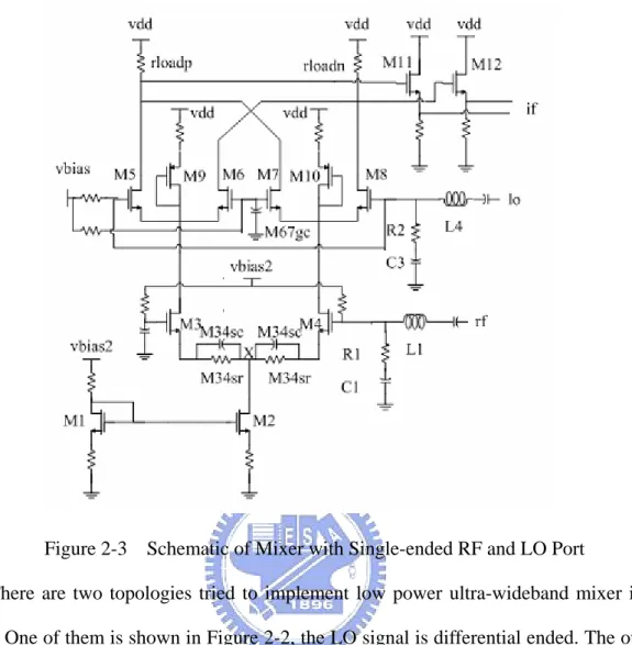
This section introduces the principles of design and the performances of ultra-wideband mixer including RF and LO matching network, P1dB, IIP3, Conversion Gain and Noise Figure. There are two circuits of mixer introduced in section 2.3.1, they are mixer with single-ended LO input and differential-ended LO inputs respectively. The advantages and drawbacks of each topology will be described in detail. We can determine which the topology is better for Ultra-Wideband Mixer from these advantages and drawbacks.
Figure 2-3 Schematic of Mixer with Single-ended RF and LO Port
There are two topologies tried to implement low power ultra-wideband mixer in this thesis. One of them is shown in Figure 2-2, the LO signal is differential ended. The other is shown in Figure 2-3, the LO signal is single ended. The mixer with single-ended LO port in Figure 2-3 is discussed first. There are some advantages and drawbacks for this topology. In advantages, there is only one LO and RF input. Therefore the RF and LO ports just need two matching networks. It can reduce the chip size and the complexity of layout. However there is a serious problem. Because the LO signal is single ended, the LO signal will feedthrough to RF terminal. Then it will be conversed down to DC by LO switching stage so that DC offset appears at two branches. It not only affects the DC level of output, but also the bias condition of M4. There are some pictures shown in Figure 2-4 to Figure 2-6, these phenomenons can be observed apparently. These figures show that the higher frequency the higher DC offset. The RF return loss is also influenced shown in Figure 2-7.
Figure 2-4 IF Output Signal RF@ 3.1GHz
Figure 2-5 IF Output Signal RF@ 7GHz
Figure 2-7 RF Return Loss
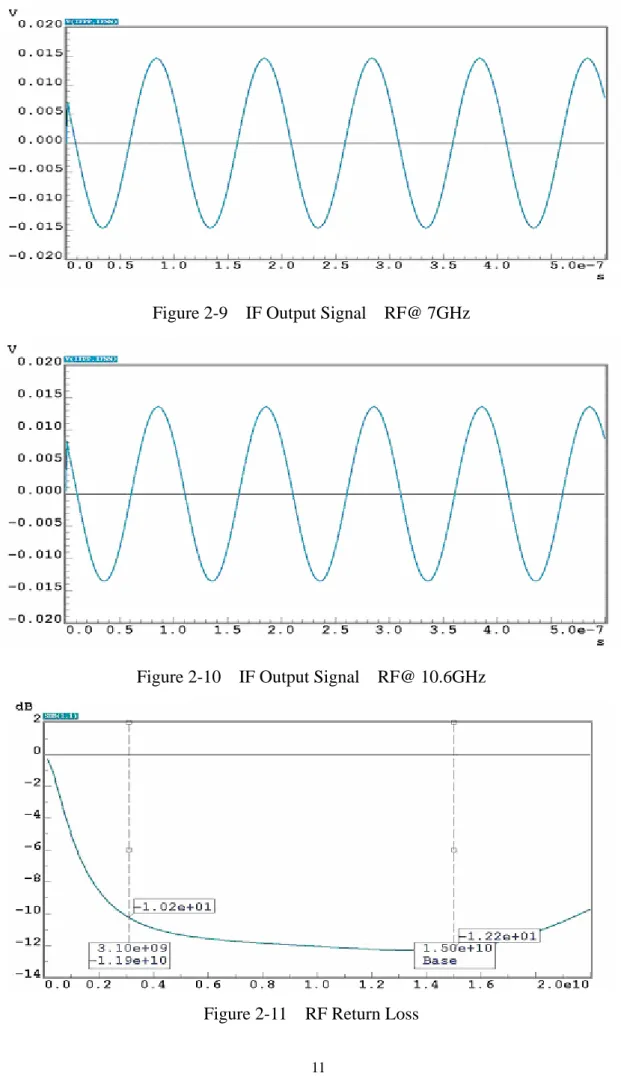
The mixer with differential-ended LO ports shown in Figure 2-2 is suitable for low power ultra-wideband mixer. It can avoid the two drawbacks of the mixer with single-ended LO port shown in Figure 2-4 to Figure 2-7. The differential-ended LO signals will reduce the feedthrough effect because LO signals will be canceled each other at RF port. It means that the LO-to-RF isolation will be improved. The DC offset and the bias voltage of M4 can be improved. And Figure 2-8 to Figure 2-11 shows the improvement after changing the topology from single-ended LO input to differential-ended LO inputs. We can see that not only the DC Offset but also the RF return loss are improved.
Figure 2-9 IF Output Signal RF@ 7GHz
Figure 2-10 IF Output Signal RF@ 10.6GHz
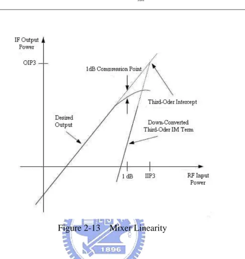
2.3.2 The RF and LO matching networks
(a) (b)
Figure 2-12 Matching Network (a) L-Shape (b) L-Shape with Resistance
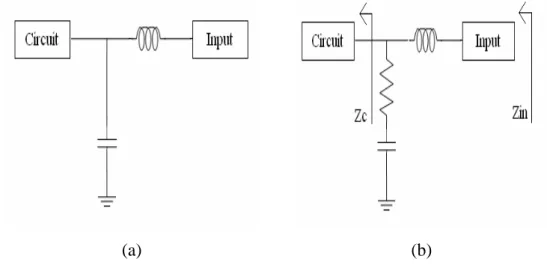
Matching network has many kinds like L-shape, Chebyshev polynomial, etc. L shape is better for this design. Because the mixer needs three matching networks for RF and LO terminals. In order to decrease the complexity and chip size, hence it must be simple structure. The L-shape matching network is the best choice like Figure 2-12 (a). However it is suitable for narrowband. The network can be changed into the topology like Figure 2-12 (b). The difference between (a) and (b) in Figure 2-12 is a resistance. This resistance can decrease the Q factor of LC matching network to achieve wideband matching. When the resistance increases, the band of matching will be wider. However the return loss will get worse. Then it must be traded off between these. From the Eq. (2.3), Zin can be designed that the RF Return Loss is better than 10 dB. However it is very hard to match the demands all the bandwidth from 3.1 to 15 GHz. The matlab software can be used to calculate the complex equations. It will facilitate the work.
SL SC R Zc Zin={ ||( + 1 )}+ RF Return Loss = 50 50 + − in in Z Z (2.3)
2.3.3
Conversion Gain
Av ≣ RF IF V V ≈ 2 1 gm∙ π 2 ∙2RL = π 2 gm RL (2.4)According the relationship of transconductance in traditional mixer architecture, which implies that the voltage gain will be portion to gm and RL. Therefore the way to increase the
voltage gain is to raise bias current or load. However the gm and load are impeded by each
other. Adding the current injection can resolve this problem [8]. Because the current provided by current injection does not go through the load to generate additional voltage drop, the gm and RL can be increased at the same time.
2.3.4
Effects of Nonlinearity
In older to simplify the analysis of nonlinearity, consider a memoryless and time-variant systems. Then the transfer function of transconductance stage can be expressed as the equation of (2.5). ... ) ( ) ( ) ( ) (t = 1x t + 2x2 t + 3x3 t + y α α α (2.5)
Considering that signal just only has a sinusoid. Setting x(t)= Acos(ωt), ... ) * cos( ) * cos( ) * cos( ) (t = A t + A2 t 2 + A3 t 3 + y α1 ω α2 ω α3 ω ... ) * 3 cos( 4 1 ) * 2 cos( 2 1 ) * cos( } 4 3 { 2 1 3 3 2 2 3 3 1 2 2 + + + + + = α A α A α A ω t α A ω t α A ω t (2.6)
In Eq. (2.6), the second term with input frequency is called the ‘‘fundamental’’ and the higher-order terms are called ‘‘harmonics’’. The parameter,α1, α2 and α3, can be
determined by the bias current. From the relation of the Vgs and bias current at transconductance stage, the values of these parameters can be got [9]. It shows that α1 and
3
1 α = 2 ssn I , α2= 0 , α3= 3 1 2 ) 2 ( 8 1 α I − ssn , k I Issn = 2 ss
Figure 2-13 Mixer Linearity
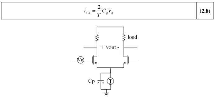
When the power of signal isn’t large enough, the circuit can amplifier the signal linearly. If the signal is large enough, the fundamental term will be affected seriously by the third harmonic terms. The conversion gain of fundamental term will be getting smaller as the input signal is getting larger. When the conversion gain decreases 1 dB, the point of P1dB will be determined by input power shown in Figure 2-13. When the linear term and the third-order intermodulation term cross, the point of IIP3 will be determined by input power shown in Figure 2-13.
In order to increase the linearity, source degeneration is usually used [10]. The nonlinearity can be improved. However the conversion gain will be decreased. It must be increased the power to maintain the conversion gain. Therefore it must trade off between the power, conversion gain and linearity. However, the noise figure will also be affected. The current injection circuit can solve this trade off relation between linearity and noise figure [11].
This is due to the fact that a large biasing current is needed for the RF input stage to achieve high gain, while a fairly low current is required for the LO switching quad to realize better noise performance.
2.3.5
Noise
The noise contribution of the loads, transconductance and switches is presented [12]. More accurate analytic methods have been represented in [13]. The principle of noise figure is discussed in A, B, C and D four parts.
A. Load Noise
Flicker noise in loads of downconversion mixer interfere the signal in zero-IF or low-IF receiver. PMOSFET has lower flicker noise than NMOSFET [14][15]. Using resistors as load in this design, which are free of flicker noise, need expense of voltage headroom.
B. Transconductance Noise
The noise in transconductance stage includes white noise and flicker noise. The white noise and flicker noise must be translated in frequency by switching stage. The flicker noise will shift the frequency ωlo and its odd harmonics, hence it doesn’t appear at IF. The white noise at ω and its odd harmonicsrf is downconverted to IF.
C. Direct Switch Noise
The direct switch noise is that the noise at the gate of switching stage interferes in the switch of switching stage. The switching stage won’t switch at the frequency ωlo. Because
noise can interfere with LO signal at zero-crossing, the switch will advance or retard. Therefore the noise goes through to IF by this effect. The output superposed with a pulse train of random width Δt and amplitude of 2I at frequency of 2ωlo. Over one period the
average value of the output current is
T S V I S V I T t I T i n n n o = × ×Δ = ×2 × =4 × 2 2 2 , (2.7)
For a sine-wave LO, S×T =4πA, where A is the amplitude of LO. However this kind of noise can be reduce to minimum by increasing the amplitude of LO. The reason can be explained from why the noise generates. It is shown in Figure 2-14. From the Figure 2-14, we can know that the higher slope of LO at zero-crossing, the fewer direct switch noise at IF.
Figure 2-14 Noise Source of Direct Switch
D. Indirect Switch Noise
The noise source as shown in Figure 2-15, , applied at the gate of the MOS will generates noise at IF output signal in two ways. First one is described in direct switch noise. The second way is introduced in indirect switch noise. The noise will charge in the Cp capacitor, hence it appears at IF by the bias current. Considering the square-wave LO, the magnitude of the current is Eq.(2.8) for zero IF.
n
V
n p n o C V T i , = 2 (2.8)
Figure 2-15 Single-balanced mixer with switch noise modeled at gate.
In general, there are two methods to reduce the Noise Figure: (1) Large LO power can suppress the noise [16] (2) Using current injection circuit to facilitate the switch of switching stage. When designing the Ultra-Wideband Mixer, the noise figure is always a troublesome problem. Considering the ultra-wideband mixer, bandwidth of the matching networks is from 3.1GHz to 15 GHz. The interferences in this bandwidth have more impacts on circuit’s performances than traditional narrowband matching. These interferences will pass through the matching networks and appear at the gates of switching stages and input transconductance stage. The interferences and white noise of transconductance stage will be translated to IF by switching stage. Also, the interferences of switching stage becomes serious by the same mechanism. Therefore the direct and indirect switch noise will get worse than those of narrow band mixer.
2.3.6
Port Isolation
Figure 2-16 LO to RF Isolation
The isolation is important element for the choice of architecture. The reason is explained in section 2.3.1. The isolation of LO-to-RF port can be increased using mixer with differential-ended LO ports. Figure 2-16 shows the isolation of RF-to-LO and LO-to-RF port. Finally, we will talk about the isolation of IF port. Although many high frequency signals will feedthrough to IF port, these effects aren’t important. Because low pass filter is usually designed at the IF port to filter these signals. From the description in section 2.3.1, mixer with differential-ended LO ports indeed have better LO-to-RF isolation than mixer with single-ended LO port.
2.3.7
Design flow
In this section the design flow of ultra-wideband mixer will be discussed in detail. When designing a mixer, the DC bias point is very important. If the DC bias point is wrong,
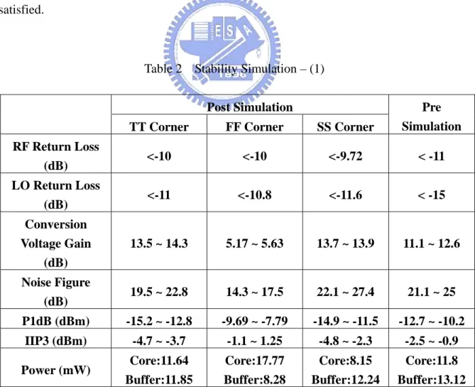
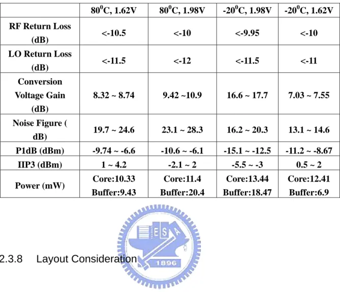
the conversion gain of the circuit will be very small. Therefore the first step is to determine the DC bias point. Then the circuit performances can be designed following the analysis from the section 2.3.1 to 2.3.6. The parameters of elements in circuit can be determined. However there is one thing, it must be noticed. It is the condition of the transistor. The condition of the transistor will determine the stability. The transistor must be designed in the condition of saturation. Some simulations about stability are shown in Table 2 and Table 3. The design of LO switching stage must be careful. The performance of noise figure and conversion gain will be decreased, if LO switching stage can’t turn on or off completely. The transistors of this stage are also designed in saturation region. Finally, adding a low-pass filter to filter the noise and buffers at IF port. These are all the design flows. If one of the performances is not satisfied, repeat the design flows until the performances are satisfied.
Table 2 Stability Simulation – (1)
Post Simulation
TT Corner FF Corner SS Corner
Pre Simulation RF Return Loss (dB) <-10 <-10 <-9.72 < -11 LO Return Loss (dB) <-11 <-10.8 <-11.6 < -15 Conversion Voltage Gain (dB) 13.5 ~ 14.3 5.17 ~ 5.63 13.7 ~ 13.9 11.1 ~ 12.6 Noise Figure (dB) 19.5 ~ 22.8 14.3 ~ 17.5 22.1 ~ 27.4 21.1 ~ 25 P1dB (dBm) -15.2 ~ -12.8 -9.69 ~ -7.79 -14.9 ~ -11.5 -12.7 ~ -10.2 IIP3 (dBm) -4.7 ~ -3.7 -1.1 ~ 1.25 -4.8 ~ -2.3 -2.5 ~ -0.9 Power (mW) Core:11.64 Buffer:11.85 Core:17.77 Buffer:8.28 Core:8.15 Buffer:12.24 Core:11.8 Buffer:13.12
Table 3 Stability Simulation – (2) 800C, 1.62V 800C, 1.98V -200C, 1.98V -200C, 1.62V RF Return Loss (dB) <-10.5 <-10 <-9.95 <-10 LO Return Loss (dB) <-11.5 <-12 <-11.5 <-11 Conversion Voltage Gain (dB) 8.32 ~ 8.74 9.42 ~10.9 16.6 ~ 17.7 7.03 ~ 7.55 Noise Figure ( dB) 19.7 ~ 24.6 23.1 ~ 28.3 16.2 ~ 20.3 13.1 ~ 14.6 P1dB (dBm) -9.74 ~ -6.6 -10.6 ~ -6.1 -15.1 ~ -12.5 -11.2 ~ -8.67 IIP3 (dBm) 1 ~ 4.2 -2.1 ~ 2 -5.5 ~ -3 0.5 ~ 2 Power (mW) Core:10.33 Buffer:9.43 Core:11.4 Buffer:20.4 Core:13.44 Buffer:18.47 Core:12.41 Buffer:6.9
2.3.8
Layout Consideration
There are many layout guidelines for high frequency RF circuits. The high frequency parasitic effects will influence the performances of design. There are several common rules: The first one is that the routes of high frequency signals must be as straight as possible. Because the more parasitic effects are generated at corners, the performances of ultra-wideband mixer will be changed. The second one is that the width of power lines must be wide enough to prevent from being burned. And the third one is that the routes of high frequency signal must be as short as possible. The parasitical capacitor from the route will affect our performance. The topology affects the parasitical capacitor, for example, the single-ended and differential-ended input mixers have one and two RF input respectively. The differential-ended input mixer needs two matching networks, it means that it has two
inductors. Because inductor has bigger area, the routes of RF signal will be extended. The topology of single RF input mixer is the better choice in this thesis. Finally, the parasitic effect of bond-wires will greatly influence the high frequency impedance matching. On wafer circuit measurement with PCB bias network is the best method. RF and LO signals are provided by 3 pins and 5 pins probe respectively. DC bias and ground are provided by the bond-wires connected to power supply. And the total chip size is 1×1 mm2. The layout is shown in Figure 2-17.
2.4
Measurement of Ultra-Wideband Mixer
2.4.1
Measurement Consideration
The operation frequency is from 3.1 to 15GHz. The bond wire will destroy the function of RF and LO input matching networks. The method of measurement must be on wafer circuit measurement with PCB bias network. The Die Photograph of UWB Mixer is shown in Figure 2-18. In order to facilitate the measurement, the length of the PCB is increased shown in Figure 2-19 and Figure 2-20. The SMA connector must be outside the plane of probe station, otherwise it can’t make the PCB connected with probe plane tightly. In addition, we need a Balun to generate differential LO signals from 3.1 to 15GHz. CIC provides two kinds of Balun. One covers 4 ~ 8GHz, the other covers 6 ~ 20GHz. The measurement can be completed by using these Baluns. The other consideration is the DC Blocking, because the DC Blocking isn’t added on chip. The measurement methods are shown in Figure 2-21. Figure 2-21 shows the methods to measure conversion gain, P1dB, RF and LO input return loss and two-tone linearity of IIP3.
Figure 2-19 PCB
Figure 2-20 Practical PCB test board of UWB Mixer
(b)
(c)
Figure 2-21 Measurement setup for (a) conversion gain (b) input return loss (c) two-tone IIP3 testing
2.4.2 Measurement Results
The power of the circuit is 23.4mW at post-simulation, when VDD is 1.8 volt. The current of the circuit is 13mA. However the current is measured about 9.695mA. Figure 2-22 shows the environment of measurement including probe station, signal generator, spectrum analyzer and DC Power Supply. The performances of measurement will be shown in this section. The DC bias points are the same as post-simulation, therefore vdd, vbias and vbias2 are 1.8, 1.3 and 1 volt respectively. In conversion power gain measurement, the RF
and LO input power are provided -40 and 0 dBm respectively. Then we can get the conversion power gain shown in Figure 2-23. We can see that the conversion power gain is from -1 to -7 dB for single IF Output. Figure 2-24 shows the conversion power gain with the power sweeping of LO. In simulation, the conversion power gain has maximum, when LO Power is -1 dBm. Figure 2-24 shows that it has maximum gain when the LO power is during -1 and +1 dBm in measurement. Figure 2-25 and Figure 2-26 show the RF and LO Return Loss in measurement. The RF return loss is better than 11 dB. The LO return loss is better than 14 dB. Then Figure 2-27 to Figure 2-30 shows the P1dB at 4, 6, 8 and 10 GHz of RF frequency. We can see that the P1dB is from -15 to -13 dBm. Figure 2-31 to Figure 2-34 shows the two-tone test. We can see that the IIP3 is from 1 to 3 dBm. Figure 2-35 to Figure 2-40 shows IF waveform and conversion voltage gain. The conversion voltage gain is shown in Figure 2-41 from differential IF ports. Table 4 shows the summaries of performance.
(a) (b) Figure 2-22 Measurement Environment
Figure 2-23 Conversion Power Gain
Figure 2-25 Return Loss of RF Port
Figure 2-27 P1dB for RF@4GHz LO@3.99GHz
Figure 2-29 P1dB for RF@8GHz LO@7.99GHz
Figure 2-31 IIP3 for RF@4GHz LO@3.99GHz
Figure 2-33 IIP3 for RF@8GHz LO@7.99GHz
(a) (b)
Figure 2-35 Measured IF Waveform (a) RF@ 4GHz (b) RF@ 5GHz
(a) (b)
Figure 2-36 Measured IF Waveform (a) RF@ 6GHz (b) RF@ 7GHz
(a) (b)
(a) (b)
Figure 2-38 Measured IF Waveform (a) RF@ 10GHz (b) RF@ 11GHz
(a) (b)
Figure 2-39 Measured IF Waveform (a) RF@ 12GHz (b) RF@ 13GHz
(a) (b)
Figure 2-41 Conversion Voltage Gain Table 4 Summaries of Performance
Specification
Simulation MeasurementVdd 1.8 1.8 Vbias 1.3 1.3 Bias Voltage (Volt) Vbias2 1 1 LO Power (dBm) -1 0 RF Return Loss (dB) < - 10 < - 10 LO Return Loss (dB) < - 11 < - 14
IF Return Loss (dB) -15 N/A
LO to RF Isolation (dB) > 80 N/A
Voltage 13 ~ 14 -0.7 ~ 6.1
Conversion
Gain (dB) Power 2.42 ~ 5.76 -7.2 ~ -1.25
Noise Figure (dB) 19.5 ~ 22.8 N/A
P1dB (dBm) - 15.2 ~ - 12.8 -15 ~ -13
IIP3 (dBm) - 4.7 ~ - 3.7 1 ~ 3
2.4.3
Comparison
Table 5 shows the comparisons of this work and other recently ultra-wideband mixer papers. The power of this circuit is very low comparing with other references. However the conversion gain isn’t flat in band like references in measurement. The power consumption reduces from 23.5mW to 17.5mW. In addition, the parasitic affects the performances of high frequency. These two factors affect the circuit performances very much.
Table 5 Comparison of Ultra-Wideband Mixer
Reference Specification
Ref. [6] Ref. [17] Ref. [4] This work
Technology 0.18um CMOS GaInp/GaAs HBT GaInp/GaAs HBT 0.18um CMOS
Supply Voltage (Volt) 5 5 5.6 1.8
Bandwidth (GHz) 0.3 ~ 25 0 ~ 8 1 ~ 17 3.1 ~ 15 Voltage -0.7 ~ 6.1 Conversion Gain (dB) Power 9.5 ~ 12.5 11 9 -1.25 ~ -7.2
RF return loss 0 ~ -10 N/A N/A < -10
P1dB (dBm) -5 -17 N/A -15 ~ -13
IIP3 (dBm) N/A -7 N/A 1 ~ 3
Noise Figure (dB) N/A N/A N/A N/A
2.5
IF Frequency Response and Circuit Netlist
Table 6 IF Frequency Response
Specification
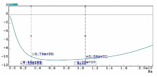
IF 100MHz IF 200MHz IF 300MHz Vdd 1.8 1.8 1.8 Vbias 1.3 1.3 1.3 Bias Voltage (Volt) Vbias2 1 1 1 LO Power (dBm) -1 -1 -1 RF Return Loss (dB) < - 10 < - 10 < - 10 LO Return Loss (dB) < - 11 < - 11 < - 11 IF Return Loss (dB) -15 -15 -15 LO to RF Isolation (dB) > 80 > 80 > 80 Voltage 13.3 ~ 14.3 13 ~ 14 12.5 ~ 13.5 Conversion Gain (dB) Power 5.13 ~ 2.15 4.42 ~ 1.47 3.45 ~ 0.53 Noise Figure (dB) 14.5 ~ 16.6 13.7 ~ 15.6 13.4 ~ 15.1 P1dB (dBm) -15.1 ~ -12.7 -14.9 ~ -12.3 -14.1 ~ -11.6 IIP3 (dBm) -4.8 ~ -2.5 -4.3 ~ -2.4 -4.4 ~ -1.7 Total Power (mW) 23.5 23.5 23.5Table 6 shows the performances at IF@ 100, 200 and 300MHz. The difference is noise figure. When the IF is higher, the noise figure is lower. Figure 2-42 shows the elements values and the currents. Figure 2-43 to Figure 2-46 shows the amplitude and phase at the nodes which are net56s and net78s in Figure 2-42. And finally, we list the circuit netlist.
Figure 2-42 The Element Values and Currents
Figure 2-44 Signal’s Phase at net56s and net78s for RF@3GHz
Figure 2-46 Signal’s Phase at net56s and net78s for RF@15GHz
Netlist
**********CURRENT MIRROR**********
xxXM1 net1d net1d net1s net1s NMOS_RF WR=4e-06 LR=1.8e-07 NR=10 m=4 xxXM1dr net1d VBIAS2 GND RPLPOLY_RF W=5e-06 L=2e-05
xxXM1sr GND net1s GND RPLPOLY_RF W=5e-06 L=3e-05
xxXM2 net2d net1d net2s net2s NMOS_RF WR=4e-06 LR=1.8e-07 NR=10 m=4 xxXM2sr GND net2s GND RPLPOLY_RF W=5e-06 L=3e-05
**********MATCHING NETWORK**********
xxX_in2l net4g INPUT GND SPIRAL_STD W=1.5e-05 S=2e-06 NR=1.5 RAD=3e-05 LAY=6 xxX_in2c net4g netr2 GND MIMCAP_WOS LT=3e-05 WT=3e-05 m=2
xxX_in2r netr2 GND GND RPHPOLY_RF W=5e-06 L=2e-06 m=2
xxX_lo2r GND netlor2 GND RPHPOLY_RF W=5e-06 L=2e-06 m=3
xxX_lo2c net58g netlor2 GND MIMCAP_WOS LT=2.4e-05 WT=2.4e-05 m=4
xxX_loL4 net58g LO GND SPIRAL_STD W=1.5e-05 S=2e-06 NR=1.5 RAD=3e-05 LAY=6
xxX_lo22r GND netlor22 GND RPHPOLY_RF W=5e-06 L=2e-06 m=3
xxX_lo22c net67g netlor22 GND MIMCAP_WOS LT=2.4e-05 WT=2.4e-05 m=4
**********TRANSCONDUCTANCE STAGE**********
xxXM4 net78s net4g net4s net4s NMOS_RF WR=4e-06 LR=1.8e-07 NR=16 xxXM4gr net4g VBIAS2 GND RPHPOLY_RF W=1e-06 L=1.2e-05
xxXM4sc net4s net2d GND MIMCAP_WOS LT=3e-05 WT=3e-05 m=4 xxXM4sr net4s net2d GND RPLPOLY_RF W=5e-06 L=5e-06
xxXM3 net56s net3g net3s net3s NMOS_RF WR=4e-06 LR=1.8e-07 NR=16 xxXM3gr net3g VBIAS2 GND RPHPOLY_RF W=1e-06 L=1.2e-05
xxXM3sc net3s net2d GND MIMCAP_WOS LT=3e-05 WT=3e-05 m=4 xxXM3sr net3s net2d GND RPLPOLY_RF W=5e-06 L=5e-06
xxXM3gc net3g GND GND MIMCAP_WOS LT=3e-05 WT=3e-05 m=4
**********LOAD**********
xxXM5gr VBIAS net58g GND RPHPOLY_RF W=1e-06 L=1.2e-05 xxXMbias1r VBIAS net67g GND RPHPOLY_RF W=1e-06 L=1.2e-05 xxXM5dr net57d VDD GND RPHPOLY_RF W=1e-06 L=4e-06
xxXM8dr net68d VDD GND RPHPOLY_RF W=1e-06 L=4e-06
**********SWITCHING STAGE**********
xxXM6 net68d net67g net56s net56s NMOS_RF WR=4e-06 LR=1.8e-07 NR=4 xxXM5 net57d net58g net56s net56s NMOS_RF WR=4e-06 LR=1.8e-07 NR=4 xxXM7 net57d net67g net78s net78s NMOS_RF WR=4e-06 LR=1.8e-07 NR=4 xxXM8 net68d net58g net78s net78s NMOS_RF WR=4e-06 LR=1.8e-07 NR=4
**********CURRENT BLEEDING**********
xxXMf8 net78s net78s netmr1 netmr1 PMOS_RF WR=5e-06 LR=1.8e-07 NR=20 m=2 xxXMmr1 netmr1 VDD GND RPHPOLY_RF W=3.7e-06 L=2e-06
xxXMf5 net56s net56s netmr2 netmr2 PMOS_RF WR=5e-06 LR=1.8e-07 NR=20 m=2 xxXMmr2 netmr2 VDD GND RPHPOLY_RF W=3.7e-06 L=2e-06
**********BUFFER**********
xxXMb2 VDD net57d IFP_PAD IFP_PAD NMOS_RF WR=5e-06 LR=1.8e-07 NR=20 m=4 xxXMbr2 GND IFP_PAD GND RPHPOLY_RF W=3e-06 L=4.8e-06 m=2
xxXMb VDD net68d IFN_PAD IFN_PAD NMOS_RF WR=5e-06 LR=1.8e-07 NR=20 m=4 xxXMbr1 GND IFN_PAD GND RPHPOLY_RF W=3e-06 L=4.8e-06 m=2
Chapter 3
C
ONCLUSIONS
A
ND
F
UTURE
P
ROSPECTS
3.1
Conclusions
A low power double balanced mixer with differential-ended LO inputs topology for multiband UWB system is presented in this report. The double balanced mixer with differential-ended LO inputs structure can decrease the DC offset, compared to the double balanced mixer with single LO input. The double balanced mixer with differential-ended LO inputs is suitable for the low power, because LO-to-RF isolation can be increased with the topology. Experimental results of the proposed mixer show some disagreements with the simulation results for multiband operation from 3.1 GHz to 15 GHz range. Especially, the conversion gain isn’t as flat as simulation. The conversion voltage gain is from 6.1 ~ -0.7 dB. Although RF return loss is also influenced, it still can be maintained better than 10 dB. The LO return loss is better than 14 dB. In linearity, there is still opportunity to improve the linearity by adding other circuit. The P1dB is -15 ~ -13 dBm from 4 GHz to 10 GHz. The IIP3 is 1 ~ 3 dBm from 4GHz to 10GHz.
In section 2.4.2, the re-simulations of modify show that the re-simulation results can approach the measurement results. The lower power consumption (17.5mW) and parasitic effects are added to the considerations of the re-simulation. Therefore the re-simulation shows that the power consumption and parasitic effects could be the elements of mismatch between simulation and measurement very much.
3.2
Future Prospects
In conclusions, the power consumption and parasitic effect influence the circuit performances. How to maintain these factors between simulation and implementation is very important. Therefore, bias circuit can be integrated into the ultra-wideband mixer in future tape out to ensure that the performances aren’t influenced by process condition. Furthermore, we must base on accurate models and careful simulation to make the measurement would close to the simulation. And the high frequency applications are the tendency. From the experiences of designing the UWB mixer, the parasitic effect is very important. However the EDA tool that we use now just can extract the resistances and capacitors. When the operation frequency is higher, the parasitic effect of inductor isn’t ignored. Therefore a more accurate and efficient EDA tool for extracting parasitic effect is quietly important.
R
EFERENCE[1] 陳慶鴻, 呂明和, 蔡文聖, 廖丁科, 「多頻帶正交分頻多工之超寬頻設計
與挑戰」,系統晶片,002 期,20~31 頁,94 年 11 月。
[2] 莊郁民, 「超寬頻技術發展剖析」,系統晶片,003 期,13~19 頁,94 年 11 月。
[3] G.Roberto Aiello, “Challenges for Ultra-Wideband(UWB) CMOS Integration,” Discrete Time Communication Inc ,San Diego,CA 92128
[4] B. Tzeng, C. H. Lien, H.Wang, Y. C.Wang, P. C. Chao, and C. H. Chen,“A 1–17-GHz InGaP-GaAs HBT MMIC analog multiplier and mixer with broad-band input-matching
networks,” IEEE Trans. Microwave Theory Tech., vol. 50, pp. 2564–2568, Nov. 2002. [5] M. D. Tsai, C. S. Lin, C. H. Wang, C. H. Lien, and H. Wang, “A 0.1–23-GHz SiGe
BiCMOS analog multiplier and mixer based on attenuation-compensation technique,” in Proc. IEEE Radio Frequency Integrated Circuits Symp., Fort Worth, TX, June 2004.
[6] Ming-Da Tsai, Huei Wang, “A 0.3 – 25- GHz Ultra-Wideband Mixer Using Commercial 0.18-um CMOS Technology,” IEEE MICROWAVE AND WIRELESS
COMPONENTS LETTERS, VOL. 14,NO. 11,NOVEMBER 2004 [7] Byoung Gun Choi, Seok-Bong Hyun, Geum-Young Tak, Tae Young Kang, Seong Su
Park,No Gil Myoung, and Chul Soon Park, “A Direct-Conversion Receiver for Low-VoltageLow-Power Multi-Band UWB with a Novel Single-Level Mixer,” Electronics and Telecommunications Research Institute (ETRI).
[8] S.-G. Lee and J.-K. Choi, “Current-reuse bleeding mixer,” ELECTRONICS LETTERS 13th April 2000 Vol. 36 No. 8
[9] Bosco Leung, VLSI for Wireless Communication, Prentice Hall Co, 2002
[10] Q. Li, and J. S. Yuan, “Linearity Analysis and Design Optimisation for 0.18um CMOS RF Mixer,” IEE Proc. Circuits Devices System, vol. 149, pp. 112-118, Apr. 2002.
[11] Bo Shi and Michael, Yan Wah Chia, “A 3.1 - 10.6 GHz RF Front-End for MultiBand UWB Wireless Receivers,” 2005 IEEE Radio Frequency Integrated Circuits Symposium. [12] H. Darabi, and A. A. Abidi, “Noises in RF-CMOS Mixers: A Simple Physical Model,” IEEE J. Solid-State Circuit,vol. 35,pp.15-25,Jan.2001. [13] C. D. Hull, and R. G. Meyer, “A Systematic Approach to the Analysis of Noise in Mixers,” IEEE J. Solid-State Circuit vol. 40, pp. No. 8
[14] J. Chang, A. A. Abidi, and C. R. Viswanathan, “Flicker Noise in CMOS Transistors from Subthreshold to Strong Inversion at Various Temperatures,” IEEE Trans. Electron Devices vol. 41, pp.1965-1971 Nov. 1994.
[15] Y. Nemironsky, I. Brouk, and C. G. Jakobson, “1/f Noise in CMOS Transistors for Analog Applications,” IEEE Trans. Electron Devices vol. 48, pp.921-927, May 2001.
[16] Behzad Razavi, RF MICROELECTRONICS ,Prentice Hall, 1998.
[17] C. C. Meng, S. S. Lu, M. H. Chiang, and H. C. Chen, “DC to 8 GHz 11dB gain Gilbert micromixer using GaInP/GaAs HBT technology,” IEE Electron. Lett., vol. 39, pp. 637–638, Apr. 2003.