氧化鋅薄膜在光電元件上的應用與研究
70
0
0
全文
(2) 氧化鋅薄膜在光電元件上的應用與研究. 研究生:林書慶 . 指導教授:張鼎張 博士. 國立中山大學 光電工程研究所碩士班. 摘要. 近年來,一些透明且導電的金屬氧化物,例如氧化鎘、氧化銦、氧化 錫和氧化鋅,已可以用於半導體上的透明薄膜,因此透明電子將是下一新 時代光電元件上應用的重要技術。 氧化鋅(ZnO)是一個II-VI族結合的半導體材料,擁有3.37 eV寬的直接能 隙,因此,氧化鋅應用在透明薄膜電晶體(TFTs)已經被廣泛地研究,而對 於氧化鋅薄膜在多樣化的應用來說,許多的製作方法也已經被嘗試在做。 在本論文中,元件的主動層為鋯摻雜氧化鋅薄膜,是使用一種溶膠凝膠 (sol-gel)以旋轉塗佈(spin-coating)的方式製作,其元件結構為底閘極底接觸 (bottom-gate bottom-contact)式的。 實驗結果得知鋯摻雜氧化鋅薄膜電晶體(ZnZrO TFTs)的電性強烈受到 可見光和周遭的氧影響。另外,關於溫度對鋯摻雜氧化鋅薄膜電晶體的電 性上影響結果也在此探討。最後,以溶膠凝膠方式製作的鋯摻雜氧化鋅薄 膜電晶體除了應用在開關元件上,在氣體感應器上的應用也具有極大潛力。 -i-.
(3) Investigation on the ZnO Thin Film for Optoelectronic Device Application. Postgraduate: Shu-Ching Lin. Advisers: Dr. Ting-Chang Chang. Institute of Dept. of Electro-Optical Engineering National Sun-Yet San University Abstract. In recent years, transparent and conductive layers of some metallic oxide, such as cadmium oxide, indium oxide, tin oxide and znic oxide, can be used for semiconducting transparent coatings. Transparent electronics are nowadays a crucial technology for the next generation of optoelectronic devices. Znic oxide (ZnO) is a II-VI compound semiconductor with a wide direct bandgap of 3.37 eV. Therefore, ZnO based transparent thin film transistors (TFTs) have been studied extensively. For the wide variety of applications, numerous ZnO films preparation methods have been attempted. In this thesis, the devices of ZnZrO active channel layers were fabricated by the sol-gel spin-coating method. These ZnZrO TFTs were fabricated by bottom-gate bottom-contact-type TFTs. The Experimental results have shown that the electrical properties of the ZnZrO TFTs are strongly dependent on visible light and ambient oxygen. In addition, in this study, the results concerning the influence of temperature on the electrical properties of ZnZrO TFTs also have been discussed. Finally, except for the application of switch devices, the ZnZrO TFTs by sol-gel spin-coating process exhibits a potential application for gas sensors.. - ii -.
(4) 誌 謝. 二年的碩士生涯過去了,對我而言,這個碩士學位不只是我一個人的努 力,而是許許多多在背後幫助我的人一起完成的。 首先感謝我的指導教授張鼎張老師。因為有您在學術上的開導與鼓勵, 讓我碩士研究期間獲得許多寶貴的知識與經驗。此外,在待人處世上的啟發 與幫助,使本人受益良多,在這裡對老師致上內心最誠摯的敬意與謝意。感 謝口試委員 朱安國教授、黃正同博士、張榮芳博士撥冗審閱,給予論文指正 與教導,特此致謝。 在實驗室方面,我要特別感謝泓緯學長在實驗上的協助及研究上的指 導,也感謝學姊美娜、學長富彥、雅喨、世青、阿飛、峰哥、大郭、小伯等 學長在我研究過程中給予建議與鼓勵,讓我對研究有更深的了解。更感謝我 可愛的團員:阿毛、阿敏、一姐、便便及信淵,讓我堅信團隊所創造的果實是 值得我們共同去回憶、去維護的,特別是阿毛開創的體育課及阿敏開創的 papago宵夜團是我碩士中經典的回憶與樂趣。還有我的同學漢博、靜美,因為 有你們陪伴,使我能在此一起成長、一起順利畢業。也感謝一精、正杰、志 豪、冠張、翊峰、煊翔、禹鈞、瑋哲、小恩、德智、侑廷、敬哲、博文等學 弟及所有支持我的朋友於研究期間,所給予的幫助及鼓勵,並一起分享生活 點點滴滴及彼此策勵,此段回憶永誌不忘。 我還要謝謝我的女朋友玥年,在精神上給我許多動力,在難過、困惑的 時候,為我加油打氣;在快樂的時候,給我無比難忘的回憶。因為有妳,讓我 對人生、對未來充滿了希望與夢想,使我能勇敢向前。 最後由衷的感謝我的父母,林錦龍先生與陳目莉女士,多年來辛苦的栽 培與教誨,並時時給我關懷與支持,使我無後顧之憂的完成我的碩士學位, 在此獻上我內心最深的謝意。 - iii -.
(5) Content Chinese Abstract……………………………………………………..i English Abstract……………………………………………………..ii Acknowledgement…………………………………………………..iii Content……………………………………………………………....iv Table Captions……………………………………………………..vii Figure Captions……………………………………………………viii. Chapter 1 – Introduction 1.1 Overview………………………………………………………….1 1.2 Motivation………………………………………………………...3 Chapter 2 – Background of znic oxide 2.1 Znic oxide.......................................................................................4 2.2 Surface conductivity and Photoconductivity..................................5 2.3 Physisorption and Chemisorption……………………………….7 2.4 Scattering mechanism…………………………………………….8 Chapter 3 – Fabrication and instruments 3.1 Device Fabrication........................................................................11 3.1.1 TFT Fabrication………………………………………………….11. - iv -.
(6) 3.1.2 Deposition of Active channel layer by spin-coating…………11 3.1.3 Baking……………………………………………………………..12 3.1.4 Patterning…………………………………………………………12 3.1.5 Annealing………………………………………………………….12 3.1.6 Film Thickness……………………………………………………13 3.2 Instruments and measurement step……………………………...14 3.2.1 Instruments………………………………………………………..14 3.2.2 Set up instruments for I-V……………………………………….15 Chapter 4 – Results and Discussion 4.1 The influence of illumination…………………………………...16 4.1.1 Experiment………………………………………………………..16 4.1.2 The influence of illumination under atmosphere…………….17 4.1.3 The influence of illumination under vacuum…………………18 4.1.4 The different wavelength of illumination……………………..19 4.2 The influence of ambient gas…………………………………....20 4.2.1 Experiment………………………………………………………..20 4.2.2 The influence of ambient gas under various pressures……...21 4.3 The steady state of the device…………………………………...22 4.3.1 Experiment………………………………………………………..22 -v-.
(7) 4.3.2 The steady state of time mode and bias mode………………..23 4.3.3 The steady state of bias mode after illumination…………….23 4.4 The influence of temperature…………………………………....25 4.4.1 Experiment………………………………………………………..25 4.4.2 The influence of temperature under atmosphere…………….25 4.4.3 The influence of termperature under vacuum………………..26 Chapter 5 – Conclusion....................................................................27 References…………………………………………………………..29 Tables…………………………………………………….………....35 Figures……………………………………………………………....37. - vi -.
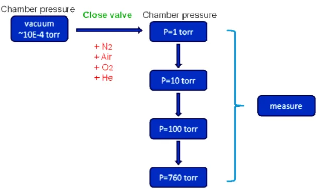
(8) Table Captions Chapter 1 Table 1.1 Some properties of transparent conducting oxides at room temperature.. Chapter 2 Table 2.1 The characteristics of physisorption and chemisorption.. Chapter 3 Table 3.1 The experimental flow chart of sol-gel precursor preparation.. Chapter 4 Table 4.1 The experimental flow chart of gas pressure in my experiment.. - vii -.
(9) Figure Captions Chapter 1 Fig. 1.1 Transfer characteristics of ZnO and Zn0.97Zr0.03O based TFTs.. Chapter 2 Fig. 2.1 The wurtzite lattice of znic oxide: small circles represent znic atoms, whereas large circles depict oxygen atoms. Fig. 2.2 The band structure of ZnO. Fig. 2.3 Lennard-Jones Model of physisorption and chemisorption; (a) physisorption of a molecule, (b) chemisorption, where at d= ∞,enough energy has been introduced to dissociate the molecule.. Chapter 3 Fig. 3.1 The device structure of Zr0.03Zn0.97O-based TFTs. Fig. 3.2 Microscope、Hot chuck、Probe station. Fig. 3.3 Agilent 4284 A、Agilent 4156C、Agilent E5250A (Switch) and Agilent 41501B (high power). Fig. 3.4 Temperature controller. Fig. 3.5 The TTP-6 Probe Station. - viii -.
(10) Chapter 4 Fig. 4.1 Transfer characteristics of ZnZrO TFTs measured repeatedly. Fig. 4.2 Transfer characteristics of ZnZrO TFTs after illuminating 10 sec and 30 min under atmosphere. Fig. 4.3 Transfer characteristics of ZnZrO TFTs illuminate by 30 min and then hold on for 5min, 1hr and 4hr under dark environment at atmosphere. Fig. 4.4 The transformation of drain current with illumination at atmosphere. Fig. 4.5 Physical model of effect of oxygen on the conductance of ZnO and the interaction with light. Fig. 4.6 Transfer characteristics of ZnZrO TFTs after illuminate by 10 sec and 30 min under vacuum. Fig. 4.7 Transfer characteristics of ZnZrO TFTs illuminate by 30 min and hold on for 5min, 1hr and 4hr at dark environment under vacuum. Fig. 4.8 Transfer characteristics of ZnZrO TFTs under different wavelength of illumination. Fig. 4.9 Transfer characteristics of ZnZrO TFTs were exposed to 1torr, 10torr, 100torr and 760torr in nitrogen. Fig. 4.10. Transfer characteristics of ZnZrO TFTs were exposed to 1torr, 10torr, 100torr and 760torr in air.. Fig. 4.11 Transfer characteristics of ZnZrO TFTs were exposed to 1torr, 10torr, 100torr and 760torr in oxygen. Fig. 4.12 Transfer characteristics of ZnZrO TFTs were exposed to 1torr, 10torr, 100torr and 760torr in helium. Fig. 4.13. The value of VT variation with pressure. Compared with nitrogen, air ,oxygen and helium for ZnZrO TFTs. - ix -.
(11) Fig. 4.14. The value of Ion variation with pressure. Compared with nitrogen, air ,oxygen and helium for ZnZrO TFTs.. Fig. 4.15. Two kinds of measurement modes (a) Time mode (b) Bias mode.. Fig. 4.16. Transfer characteristics of ZnZrO TFTs under the time mode. (Time mode). Fig. 4.17. Transfer characteristics of ZnZrO TFTs under the bias mode. (Bias mode). Fig. 4.18. The value of Ion variation in time. Compared with Time mode and Bias mode for ZnZrO TFTs.. Fig. 4.19. The value of VT variation in time. Compared with Time mode and Bias mode for ZnZrO TFTs.. Fig. 4.20. Transfer characteristics of ZnZrO TFTs under Bias mode after 30s of illuminate at atmosphere.. Fig. 4.21. The transformation of drain current under Bias mode at atmosphere.. Fig. 4.22. Transfer characteristics of ZnZrO TFTs under Bias mode after 30s of illuminate at vacuum.. Fig. 4.23. The transformation of drain current under Bias mode at vacuum.. Fig. 4.24. Output characteristics of ZnZrO TFTs at temperatures from 30℃ to 125℃ under atmosphere.. Fig. 4.25. Transfer characteristics of ZnZrO TFTs at temperatures from 30℃ to 125℃ under atmosphere.. Fig. 4.26. Output characteristics of ZnZrO TFTs by first measured at temperatures from 30℃ to 125℃ under atmosphere.. Fig. 4.27. Transfer characteristics of ZnZrO TFTs by first measured at temperatures from 30℃ to 125℃ under atmosphere.. Fig. 4.28. Output characteristics of ZnZrO TFTs were measured by 5 times at -x-.
(12) temperature 125℃ under atmosphere. Fig. 4.29. Output characteristics of ZnZrO TFTs at temperatures from 30℃ to 125℃ under vacuum.. Fig. 4.30. Transfer characteristics of ZnZrO TFTs by first measured at temperatures from 30℃ to 125℃ under vacuum.. - xi -.
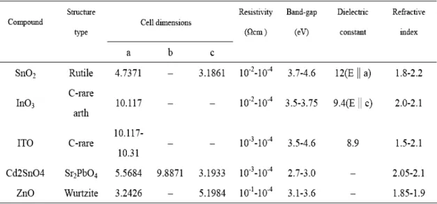
(13) Chapter 1 Introduction 1.1 Overview Transparent electronics are nowadays an emerging technology for the next generation of optoelectronic devices. Oxide semiconductors are very interesting materials because they combine simultaneously high/low conductivity with high visual of application (e.g. antistatic coatings, touch display panels, solar cells, flat panel displays, heaters, defrosters, optical coatings, among others) for more than a half-century. Transparent and conductive layers of some metallic oxide, such as cadmium oxide, indium oxide, tin oxide, and znic oxide, can be used for semiconducting transparent coatings. Some of the properties of these materials are show in Table 1.1 [1.1]. Therefore, znic oxide (ZnO) is a transparent conducing oxide (TCO), which has recently been studied extensively. It is a II-VI compound semiconductor, mostly n-type, with a hexagonal wurtzite structure and a wide direct band gap of ~3.3eV, that could be obtained with resistivity as low as 10-6 Ω‧m. It is a candidate material for use as a gas sensor, in electronic displays, in fabrication of blue light emitting diodes (LEDs), in surface acoustic wave (SAW) devices, and more. In addition, the ZnO films have been deposited using many methods of deposition techniques. These include various sputtering techniques [1.2,1.3], chemical vapor deposition (CVD) [1.4], molecular beam epitaxy (MBE) [1.5], pulsed laser deposition (PLD) [1.6], sol-gel [1.7,1.8], and more. Recently, high-performance thin-film transistors (TFTs) based on new materials have been investigated to achieve the features of larger diagonal size, greater transparency, more pixels, and lighter weight for high resolution electronic display devices [1.9,1.10]. The most commonly used material for the active 1.
(14) channel layer are amorphous a-Si:H and polycrystalline silicon poly-Si. However, there are a number of drawbacks associated with both of these materials. While poly-Si devices have a high mobility 50 cm2V-1S-1, the thermal budget needed for their production makes them somewhat incompatible with flexible substrates based on polymers. In addition, poly-Si can be difficult to fabricate over large areas. Conversely, a-Si:H is readily used in large area flat panel displays but demonstrates a shortcoming, such as reduced pixel brightness due to opaque a-Si material. To date, transparent oxide semiconductor based transistors have been proposed using as active channel non-doped ZnO [1.11,1.12]. The ZnO-based TFTs have been intensively studied due to their larger deposition area, non-toxicity, and high transparency as well as their compatibility with glass and plastic substrates, low-temperature processing, and simple wet chemical etching [1.12,1.13]. These advantages of ZnO thin films have driven research efforts to develop high-performance ZnO TFTs to overcome shortcomings of conventional a-Si TFTs. Hence, in this study, the devices of ZnZrO active channel layers were fabricated by the sol-gel spin-coating method. Sol-gel derived mixed oxide films also attracted attention of many researchers working in this field due to its simplicity, cost effectiveness and advantage for large area deposition. The mixed oxide of Zn and Zr are very rarely studied and might be interesting from the point of view of application. With this understanding, we have fabricated mixed oxide of Zn and Zr films using sol–gel spin-coating method. It is an attractive technique for obtaining thin films and has the advantages of easy control of the film composition and fabrication of a large area thin film with low cost. Therefore, in the present study, the results concerning the influence of time, visible light, ambient gas and temperature on the electrical properties of ZnZrO TFTs, representing four of the key factors that TFTs have to deal with when they are used in conventional electronic applications.. 2.
(15) 1.2 Motivation Znic oxide (ZnO) is a transparent conducing oxide (TCO) which has very popularly used due to its unique optical and electronic properties in solar cells, photo detectors, light emitting devices, gas sensor elements, and surface acoustic wave guides. Recently, ZnO utilized as active channel layers (ACLs) in thin film transistors (TFTs) have attracted much attention due to its exhibiting n-type semiconductor characteristic with wide band gap of 3.3 eV, excellent chemical and thermal stability, and can be well-oriented crystalline on various substrate. In this study, the devices of Zr-doped ZnO ACLs were fabricated by sol-gel process through spin-coating deposition method. Fig.1.1 shows electronic properties of ZnO and Zn0.97O Zr0.03 based-TFTs, the off-current of Zr-doped ZnO films TFTs is lower than non-doped ZnO films TFTs. In addition, the sol-gel process has been an attractive technology which is simple and low cost for depositing devices and low cost than vacuum techniques. Therefore, the results concerning the influence of time, visible light, ambient gas and temperature on the electrical performance of sol-gel derived Zr-doped ZnO films TFTs are discussed.. 3.
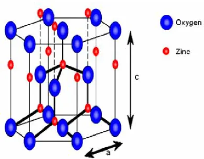
(16) Chapter 2 Background of Znic oxide 2.1 Znic oxide Znic oxide is a II-VI n-type wide band gap semiconductor; band gap Eg = 3.2~3.3 eV at room temperature. Znic oxide crystallizes in hexagonal wurtzite lattice. The znic atoms are nearly in the position of hexagonal close packing. Every oxygen atom lies within a tetrahedral group of four znic atoms, and all these tetrahedral point in the same direction along the hexagonal axis giving the crystal its polar symmetry. The wurtzite lattice of znic oxide is shown in Fig. 2.1 the lattice constants are a=3.24 Å and c=5.19 Å. The band structure of ZnO has been calculated by using a Hartree-Fock-Slater Hamiltonian employing an oxygen non-local ionic high symmetry lines in the hexagonal Brillouin Zone [2.1]. A typical band structure is shown in Fig. 2.2. The lowest two valence bands occurring at approximately -20 eV correspond to O:2s core-like states. The next six valence bands from -6 eV to 0 eV correspond to O:2p bonding states. The first two conduction band states are strongly localized on Zn and correspond to unoccupied Zn:3s levels. The higher conduction bands are fairly free-electron-like. The bulk electronic properties of ZnO are described by a tight bonding Hamiltonian obtained by fitting self-consistent pseudopotential bulk band structure. The surface band structures have been calculated using the scattering theoretical method. The Hamiltonian includes first and second nearest-neighbor interactions, namely Zn:4s and O:2p orbital. In undoped znic oxide the n-type conductivity is due to deviations from stoichiometry. The free charge carriers result from shallow donor levels associated with oxygen vacancies and interstitial znic [2.2], although interstitial oxygen and 4.
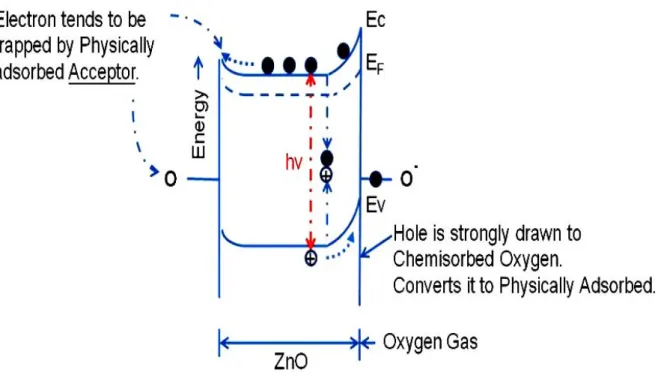
(17) znic deficiencies may also be present and produce acceptor states [2.3]. Regardless of the deposition method, all undoped ZnO conducting films have unstable electric properties in the long term. This stability is related to the change in surface conductance of ZnO films under oxygen chemisorptions and desorption [2.4]. The electrical properties of ZnO films strongly depend on the deposition method, thermal treatment and oxygen chemisorptions.. 2.2 Surface conductivity and Photoconductivity In general, a semiconductor absorbs light with energy higher than the band gap energy, electron-hole pairs are generated according to Eq. (2-1), +. hv → h + e. −. (2-1). effectively resulting in the increase of electrical conduction which may be a fundamental,. solid-state. process. for. photoconduction. of. conventional. semiconductors. The electron and holes generated by light absorption rapidly vanish after turning off the light. Therefore, the photoresponse, namely, rise in conductivity upon light illumination and the decay after cutting off light, due to the solid-state process, is expected to be very rapid. For the last two decades it has been well known that the photoresponse of n-type metal oxide semiconductors such as titanium and znic oxides shows a slow conduction decay process, as opposed to the rapid solid-state process, which is controlled by surface effects such as gas adsorption and desorption [2.5,2.6]. In the dark, an oxygen gas adsorbs on the oxide surface as a negatively charged ion by capturing free electrons of the n-type oxide semiconductor, as described by Eq.(2-2), −. O2 ( g ) + e → O2 (ad ). (2-2). thereby creating a depletion layer with low conductivity near the surface. When 5.
(18) light with energy higher than the fundamental absorption band of the semiconductor is illuminated, holes which are produced by light absorption near the surface migrate to the surface along the potential slope created by band bending and discharge the negatively charged adsorbed oxygen ions. +. −. h + O2 (ad ) → O2 ( g ). (2-3). Electrons produced at the same time by the light destruct the depletion layer, increasing the conductivity [2.7]. Thus the photoresponse of oxide semiconductors includes adsorption Eq. (2-2) and photodesorption of oxygen on the surface Eq. (2-3) in addition to the very rapid change in conductivity by photogenerated hole-electron pairs and their extinction, which is, in other words, the solid-state process Eq. (2-1). Consequently, the decay of photoconduction is strongly dependent on the ambient gas conditions, being slow in vacuum or an insert gas atmosphere such as nitrogen, and fast in air [2.8]. Collins and Thomas further proposed that an electron enriched-type space-charge layer is formed by the photolysis of the znic oxide (single crystal) surface. The holes from hole-electron pairs generated by light absorption discharge surface lattice oxygen ions leaving an excess of znic (interstitial) near the surface, according to Eq. (2-4). 2+. 2−. Zn (c) + O (c) + 2hv → 1 / 2O2 ( g ) + Zni.. (2-4). Ionization of interstitial znic by Eq. (2-5) affords free carrier electrons. +. Zn i → Zn + e. −. (2-5). It is very interesting to investigate the photoconductive properties of ultrathin films of n-type oxide semiconductors, because it can be assumed that they have some special photoelectrical properties due to the higher ratio of their surface atoms compared to bulk materials. 6.
(19) 2.3 Physisorption and Chemisorption There are two major classifications of adsorption shown in Table 2.1: physisorption (weak bonding, heat of adsorption is less than about 6 kcal mol-1) and chemisorption (strong bonding, heat of adsorption is usually greater than about 15 kcal mol-1). Fig. 2.3 is the Lennard-Jones representation of physisorption and chemisorption. The Lennard-Jones model is a simple way to visualize the development of the activation energy ΔEA of chemisorption. This is the energy that must be supplied to a molecule before it will chemisorb. Consider, with Fig. 2.3, a molecule approaching the solid, with the total energy zero as indicated in curve a (the physisorption curve). It is not necessary to provide the total energy of dissociating the molecule before it can chemisorb; a lesser energyΔEA suffices when the molecule is near the surface, where in the Lennard-Jones model the curves for physisorption and chemisorption intersect. Thus the rate of adsorption (assuming modest coverage) is. dθ ⎛ − ∆E A ⎞ = κ ads exp⎜ ⎟ κ dt T ⎠ ⎝. (2-6). where θ is the fraction of available surface sites covered. Equation (2-6) represents the rate for the normal case where ΔEA is provided thermally. In this case, by Eq. (2-6), at very low temperature chemisorption cannot realistically occur. A chemisorbed species can interact more strongly with the solid, and the interaction is best described as the incipient formation of a new phase. In principle during physisorption and chemisorption of an adsorbate (the adsorbing species), there is no movement of the atoms of the adsorbent (the solid) from their normal lattice position. In practice, especially with chemisorption, there is movement and relocation of the surface atoms. One can view incipient formation of a new phase as the point where the surface atoms of the adsorbent change their bond structure, breaking bonds to the solid and replacing them with bonds to the adsorbate. It will 7.
(20) not dwell on new phase development-the processes are hard to define quantitatively in practical cases, although with the new surface spectroscopies such as LEED (low-energy electron diffraction) the progress from simple adsorption to a new surface phase can be followed. It will instead concentrate on the description of adsorption, emphasizing the form most basic to gas sensors-ionosorption, adsorption as a surface state, where charge is transferred from the conduction or valence bands to ionize the adsorbate, but where local bonding of the adsorbate to one or a few atoms of the solid can be ignored. The dependence of the rate of physisorption and chemisorption on the pressure of the species in the gas phase can be complex; there are many expressions, both analytical and empirical, describing the dependence. In most of the discussion to follow we will assume the simple Henry’s law, namely that the rate is proportional to the pressure. This law applies reasonably well at low coverage of the surface, but is inadequate as one approaches a monolayer.. 2.4 Scattering mechanism It is a fact that generally the resistivity of the films prepared by sol–gel method is sufficiently low prepared by other chemical methods like chemical vapor deposition [2.9,2.10] but still higher than those prepared by other methods like sputtering technique. Thus, the effect of other factors like defect association, stresses in film, thermal expansion mismatch with the substrate and chemical changes especially for sol–gel films cannot be ruled out [2.11]. According to Orton and Powell [2.12] if the average grain size is larger than 2LD where LD is Debye screening length, the potential barrier exists. Here LD is given by. LD. ⎛ εε kT = ⎜ 02 ⎜ ⎝ e n. ⎞ ⎟ ⎟ ⎠. 1/ 2. (2-7). 8.
(21) where ε is the static dielectric constant, εo , permittivity of free space and n the carrier concentration. As n~1017, LD~10 nm which is less than crystallite size (L) as estimated from XRD measurements or the grain size as evaluated from SEM study. The main transport between neighboring grains might be by thermionic emission over the barrier and tunneling effect across the barrier. The conductivity by thermionic emission σth over the back to back Schottky barrier is given by 2. σ th =. Le n * ⎞ ⎛ 2 π m kT ⎟ ⎜ ⎠ ⎝. 1/ 2. ⎛ − EB ⎞ exp⎜ ⎟ ⎝ kT ⎠. *. where n is the carrier concentration, m. (2-8). the effective mass, k the Boltzmann. constant and EB is the barrier height. The contribution to the conductivity is thermally activated with a barrier height EB determined by the band edge mismatch and by the position of the Fermi level. From Eq. (2-8). σ = enµ 0T. −1 / 2. ⎛ − EB ⎞ exp⎜ ⎟ kT ⎝ ⎠. (2-9). Where. µ0 =. Le *. (2-10). 1/ 2. ( 2πm k ). Has been approximated as. σ = enµ. (2-11). Where, the mobility. µ = µ 0T. −1 / 2. ⎛ − EB ⎞ exp⎜ ⎟ kT ⎝ ⎠. (2-12). So, the barrier height can be obtained from a plot of ln(μT1/2) versus l/T curve. Thus, the high temperature region corresponds to thermionic emission but for 9.
(22) temperature lower than 200K the conductivity deviates from Arrhenius plot. This region might correspond to the tunneling process across the barrier. The criterion for a current dominated by tunneling is that the parameter Eoo, which determines the energy where most of tunneling occurs, is much larger than kT. The parameter Eoo is given by [2.13]. E oo = 18.5 × 10. −12. ⎛ n ⎞ ⎟ ⎜ ⎝ m *ε ⎠. (2-13). Where n is the carrier concentration. Assuming n = 1017cm-3, in ZnO films m*= 0.35m and ε= 8.5, E00 can be calculated as 0.025 eV from Eq. (2-13), i.e E00 = kT where T is the room temperature. As a result mobility is limited by both thermionic and thermal field emission of electrons at room temperature. If the semiconductor is at high temperature or in a low doping range where kT≧E00, then the mobility is dominated by the thermionic emission of electrons over the grain boundary barriers. On the other hand, if the semiconductor is at low temperature or in a high doping range where kT < E00, then the mobility is limited by the thermal field emission of electrons through the grain boundary barriers.. 10.
(23) Chapter 3 Fabrication and Instruments 3.1 Device Fabrication 3.1.1 TFT Fabrication In order to make sure the Zn1 − xZrxO TFTs have lower off current, we demonstrated the Zn1 − xZrxO-based TFT with a conventional structure, to fabricating easily and efficiently. The device structure of Zn1−xZrxO based -TFTs as shown in Fig. 3.1 is the bottom-gate type and was fabricated by the following sequence of processes. The metal MoW was deposited on the glass substrate as a bottom gate electrode. Silicon nitride served as the gate insulator with a thickness of 3000 Å. The source and drain electrodes were made up of indium-tin oxide (ITO) and channel width and length were 500 and 50 μm, respectively. Finally, the Zn1− xZrxO. thin films were deposited by spin-coating with the processing parameters.. The device structure of Zn1−xZrxO -TFTs in bottom-gate type were fabricated by the Taiwan TFT LCD Association (TTLA). The Zn1−xZrxO film were fabricated by spin coater in the National Nano Device Laboratories (NDL).. 3.1.2 Deposition of Active channel layer by spin-coating Table 3.1 shows experimental flow chart of sol-gel precursor preparation. The Zn1 −. xZrxO. sol-gel precursors were synthesized by the mixing of znic acetate. {Zn(CH3COO)2 · 2H2O} and zirconium isopropoxide {Zr[(CH3)2CHO]2} dissolved in 2-methoxyethanol and monoethanolamine (MEA), and the solutions were stirring at 60°C for 30 min. The nominal x value for Zn1−xZrxO is 0.03. Zn0.97Zr0.03O thin films were deposited using the sol-gel solution by the spin-coating method. After coating, the films were immediately baked at 300°C for 11.
(24) 10 min on the Hot-plate. The rotation rate of the spin coater is 400 rpm, 15 seconds for step1 and 2000 rpm, 20 seconds for step 2.. 3.1.3 Baking After deposited by spin coating, the films were dried at 300°C for 10 min over a hot plate to evaporate the solvent and remove organic residuals. The procedures from coating to drying were only one times until the desired thickness of the sintered films was reached.. 3.1.4 Patterning There are many scientific or technical literatures which report HCl and HNO3 can etch ZnO films, but the etching rate of HCl and NHO3 solution is too fast for the Zn0.97Zr0.03O films. It will damage the Zn0.97Zr0.03O pattern and exhibit a lateral etching phenomenon. So, it mixed with the CH3COOH as buffer solution to reduce the etching rate. The optimal solution rate as H2O: CH3COOH: HCl/HNO3 : = 1 : 2 : 40. HNO3 for the Zn0.97Zr0.03O films is main etching solution. In this section, Zn0.97Zr0.03O films are patterned by photolithography and wet-etching with the solution mention above.. 3.1.5 Annealing The electrical characteristic of Zn0.97Zr0.03O-based TFTs are closely related to its crystal structure and oxygen vacancies (Vo), which can be controlled by doping or annealing conditions in oxygen atmosphere. In general, the intrinsic defects in ZnO films include oxygen vacancy (Vo), interstitial znic (Zni), etc. However, these defects can affect the electron concentration. The influence of oxygen vacancies (Vo) on the conductivity of the Zn0.97Zr0.03O has been confirmed in the annealing temperature. For Zn0.97Zr0.03O thin film, the change in the concentration of the oxygen vacancy (Vo) could lead to the change of the electron concentration and 12.
(25) hence make the bulk change from semiconductor to conductor. In this section, vacuum annealing furnace was used as annealing equipment and samples were used annealing temperature at 350°C for 1 hr under oxygen ambient 0.6 torr for TFTs.. 3.1.6 Film Thickness In general, the physical characteristics of polycrystalline semiconductors are easily modified by their crystallite sizes and boundary effects. The electrical properties are much more easily disturbed as long as the band structure altered inside the crystallites from the optical properties. The size of crystallites and the magnitude of the associated grain-boundary effects are dependent upon the preparation and treatment method, such as temperature in deposition or annealing, sputtering process, and deposition technique. In this section, the Zr0.03Zn0.97O films were prepared by spin-coating with 2 times and the thickness about 1100~1200 Å.. 13.
(26) 3.2 Instruments and measurement setup 3.2.1 Instruments (1) Microscope、Probe station, as shown in Fig. 3.2. (2) Agilent 4284A、Agilent E5250A (Switch) and Agilent HP4156C. , as shown in Fig. 3.3. (3) Temperature controller, as shown in Fig. 3.4. (4) TTP-6 Probe Station, as shown in Fig. 3.5. (5) Software of measurement. ICS(Interactive Characterization Software). Use the software to get :. VDS-IDS. VGS-IDS (Linear Region). VGS-IDS (Saturation Region). VGS-Gm. 14.
(27) Note:VDS : Drain voltage IDS : Drain current. VGS : Gate voltage. IGS : Gate current. Gm : VGS - IDS max slope. 3.1.2 Set up instruments for I-V The current – voltage characteristic measurement of thin film transistor devices was performed by HP4156C semiconductor characterization system with source grounded and body floating. The electrical test setup of HP4156C semiconductor characterization system, illustrated at Fig. 3.3, a probe station situated inside a dark box. The ground probe station is furnished with an electrically isolated, thermal chuck. The chuck is controlled by LakeShore 331 thermal controller, which can operate temperature from 77K to 400K. A semiconductor characterization system of Agilent HP4156C provides I-V measurement, bias for BTS. The HP4156C are connected to B2201A low leakage switch mainframe, and then link to dark box. The current-voltage (I-V) characteristics measurements were gotten by using n-TFT and p-TFT structure with Agilent HP4156C semiconductor characterization system. Agilent HP4156C can measure the minimum leakage current: 1f (A).. 15.
(28) Chapter 4 Results and Discussion In this chapter, the results of four subjects concerning the influence of illumination, ambient gas, steady state and temperature on the electrical characteristics of ZnZrO TFTs are discussed. Fig. 4.1 shows the VG-ID transfer characteristic of the ZnZrO TFTs in continuous measurement. It is seen a special phenomenon, in order to make the ZnZrO TFTs reach the steady state, the electrical characteristics of the ZnZrO TFTs have been measured 10 times. The threshold voltage (VT) and on-current (Ion) for 10 times measurements were obviously different with the first measurement. It is assumed that the electrical characteristics of ZnZrO TFTs depend on ambient environment. Therefore, on the purpose of reaching the steady state of the ZnZrO TFTs in next experiment, the repeated measurement is needed.. 4.1 The influence of illumination 4.1.1 Experiment In this section, there are three subjects to be discussed: (1) The influence of illumination under atmosphere. (2) The influence of illumination under vacuum. (3) The different wavelength of illumination. We set up an experiment to measure I-V characteristics by using a HP4156C semiconductor parameter analyzer. First, the steady state of ZnZrO TFTs is measured repeatedly under dark at atmosphere, this is the standard electrical characteristics of ZnZrO TFTs. Second, the VD-ID and VG-ID in saturation regime (VD=30V) are measured after illuminating 10 sec. and 30 min. at atmosphere. Then 16.
(29) the light turned off and measured electrical characteristics of ZnZrO TFTs after illumination under dark with different time, including 5min, 1hr and 4hr. Next, compare the electrical characteristic of ZnZrO TFTs at vacuum and atmosphere in the same measured conditions. In the last subject, the VD-ID and VG-ID in saturation regime (VD=30V) are measured by different wavelength of illumination.. 4.1.2 The influence of illumination under atmosphere Fig. 4.2 shows the VG-ID transfer characteristics of ZnZrO TFTs after illuminating 10 sec. and 30 min. under atmosphere. It shows that the characteristics of ZnZrO TFTs were influenced by illuminated time. The on-current (Ion) and off-current (Ioff) were also increased with illumination time. It is apparent that the electrical characteristics of ZnZrO TFTs transfer to conductor after 30min of illumination. It shows that the ZnZrO TFTs is very photo-sensitive to illumination time. Especially, the on/off ratio of ZnZrO TFTs varies significantly with the increase of illumination time. This is photoconductivity phenomenon that show to be entirely due to desorption of chemically adsorbed oxygen atoms from the surfaces of the porous sample [4.1]. This indicates that the light of intensity near the fundamental absorption edge forms electron-hole pairs of which the hole is captured by the oxygen on ZnO surface, converting the oxygen to physically adsorbed as time increasing [4.2,4.3]. Fig. 4.3 shows the VG-ID transfer characteristics of ZnZrO TFTs illuminate by 30min and then hold on for 5min, 1hr and 4hr under dark environment at atmosphere. It shows that the characteristics of ZnZrO TFTs were influenced by relaxation time, which recovers to standard electrical characteristics of ZnZrO TFTs. The on-current (Ion) and off-current (Ioff) were decreased with relaxation time. 17.
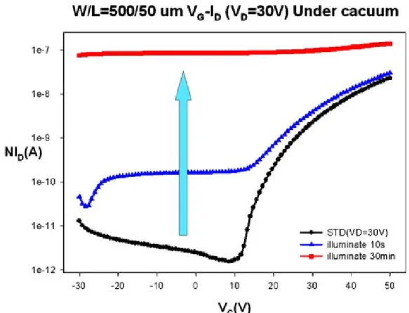
(30) It is apparent that the electrical characteristics of ZnZrO TFTs due to the conductor transfer to transistor after 4hr of relaxation under dark and closer to the standard. This indicates that the oxygen is chemisorbed to ZnO surface at vacancy sites, forming O2- as increase as relaxation time increasing and resulting in a surface charge depletion layer thus leading to a reduction of the electrical conductivity and the I-V can be transferred to transistor characteristics [4.4]. Fig. 4.4 shows the transformation of drain current with illumination of 15min. It shows that the drain current of ZnZrO bulk was influenced by illumination time and relaxation time. The plot also represents that the conductivity of ZnZrO bulk was influenced by illumination time and relaxation time. Fig. 4.5 shows the physical model of effect of oxygen on the conductance of ZnO film and the interaction with light [4.1]. The increase of conductivity under illumination indicates capture of holes at grain boundaries, which are negatively charged in darkness, and a corresponding number of excess electrons are left in the conduction band. The decrease of conductivity under dark indicates that oxygen in air caused an appreciable decrease in the steady state photoconductivity of the ZnO film [4.5].. 4.1.3 The influence of illumination under vacuum Fig.4.6 shows the VG-ID transfer characteristics of ZnZrO TFTs after illuminating by 10s and 30min under vacuum. It also shows that the characteristics of ZnZrO TFTs were influenced by illumination time. Compare to the plot in Fig. 4.2, the VG-ID transfer characteristics of ZnZrO TFTs showed similar trends. The drain current of ZnZrO TFTs at vacuum was larger than that at atmosphere, where higher conductivity obtained under illumination continued for 30min even after extinguishing the light. In our previous study, we have investigated the photoconductivity effect of the ZnO to realize how the oxygen will influence the 18.
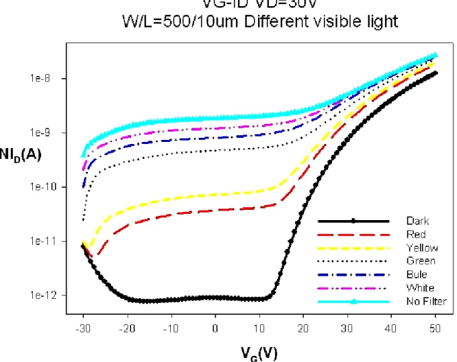
(31) performance of the ZnZrO TFTs. Fig. 4.7 shows the VG-ID transfer characteristics of ZnZrO TFTs illuminate by 30min and then hold on for 5min, 1hr and 4hr under dark environment at vacuum. Especially, the electrical characteristics of ZnZrO TFTs illuminate by 30min after 4hr relaxation at vacuum still show a conductor characteristic. Compare to the plot in Fig. 4.3, the recovery of the device at vacuum is less than the device at atmosphere. It is a contrary result to illumination data for the ZnZrO TFTs at atmosphere and the ZnZrO TFTs at vacuum. Consequently, the ZnZrO TFTs is more photo-sensitive to illumination at vacuum than at atmosphere, cause to the physically adsorbed oxygen easily desorbs and the electron remains to increase the conductivity. In addition, we can infer that the devices of ZnZrO active channel layers were fabricated by the. sol-gel spin-coating method may have much porous. Through this pores, oxygen gas may diffuse rather freely into the interior part of the ZnZrO film from the surface. It indicates that the result obtained in this study is that the oxygen reacts with the electron under atmosphere is more than under vacuum.. 4.1.4 The different wavelength of illumination Fig. 4.8 shows the VG-ID transfer characteristics of ZnZrO TFTs under different wavelength of illumination. The on-current (Ion) and off-current (Ioff) were increased with the light of wavelength reduce. The general trend as wavelength decrease is a decrease in the on/off ratio of ZnZrO TFTs. When the transfer characteristics are measured with incident monochromatic light and as wavelength decreases, several changes in the electrical properties of the ZnZrO TFTs are verified as can be seen in Fig. 4.8. It is well-known the energy of the photons (less than 2 eV) is too low to be absorbed by the ZnZrO film that has an optical bandgap 19.
(32) around 3.2 eV [4.6], it is apparent that the ZnZrO TFTs is very photo-sensitive to illumination and also represents the ZnZrO films have traps, cause to emerge evidently the phenomenon. This reason of a factor among them is the same to photodesorption as previously mentioned, which is that the light of intensity near the fundamental absorption edge forms electron-hole pairs of which the hole is captured by the oxygen on ZnO surface, converting the oxygen to physically adsorbed as decrease as wavelength. Then the conductivity obviously increased that the electron concentration increases in bulk. In other words, we inferred that the light with energy higher than the fundamental absorption band of the ZnZrO film is illuminated lead to a rise of photogenerated hole-electron pairs as the wavelength reducing [4.7,4.8].. 4.2 The influence of ambient gas 4.2.1 Experiment In this experiment, we also discuss the four kinds of ambient gas on the ZnZrO TFTs under various gas pressures, including 1 torr, 10 torr, 100 torr and 760 torr. The kinds of gas are nitrogen, air, oxygen and helium specifically. Table 4.1 shows experimental flow chart of gas pressure. First, the ambient air was pumped out reach to ~10-4 torr and subsequently close valve. Second, the VD-ID and VG-ID in saturation regime (VD=30V) were measured under the pressure of 1torr, 10 torr, 100torr and 760 torr while fill the ambient gas.. 20.
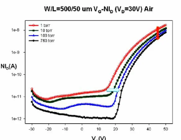
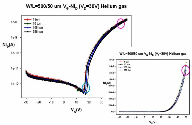
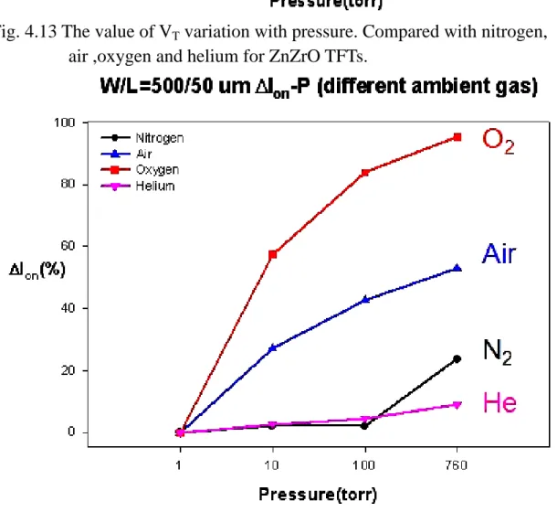
(33) 4.2.2 The influence of the ambient gas under various pressures Fig. 4.9 shows the VG-ID transfer characteristics of ZnZrO TFTs exposed to various pressures from 1torr to 760torr in nitrogen. As the plot, on-current and threshold voltage of ZnZrO TFTs are varied not obvious. Addition, Fig 4.10 and 4.11 plot the VG-ID relationships of ZnZrO TFTs were exposed to various pressures from 1torr to 760torr in air and oxygen, respectively. As the result, these indicate the device characteristics of ZnZrO TFTs are strongly dependent on oxygen. It also shows on-current and threshold voltage degraded more seriously as the magnitude of oxygen increased. This is the main reason of these chemisorbed O2- deplete the electron states from surface and reduce the conductivity of bulk. Besides, Fig. 4.12 shows the VG-ID transfer characteristics of ZnZrO TFTs exposed to various pressures from 1torr to 760torr in helium. It also shows similar trend with the plot of Fig. 4.9. This is due to that helium is an inert gas, and which would not combine with other atoms. Consequently, Fig. 4.13 and Fig. 4.14 show the value of VT and Ion variation with pressure, respectively. It indicates that the decay of photoconduction is strongly dependent on the ambient gas conditions, being slow in inert gas such as nitrogen or helium, and fast in air or oxygen [4.4]. The electrical performances of ZnZrO TFTs were seriously degraded as the magnitude of oxygen increased.. 21.
(34) 4.3 The steady state of the device 4.3.1 Experiment In our previous study, in order to make the ZnZrO TFTs reach to a steady state that is measured repeatedly under dark at atmosphere. Hence, it is separated into two kinds of measurement conditions to discuss the steady state of ZnZrO TFTs : (1) The steady state of time mode and bias mode. (2) The steady state of bias mode after illumination. We set up an experiment to measure I-V characteristics by using a HP4156C semiconductor parameter analyzer. First, the I-V of ZnZrO TFTs was measured by hold on 30min under dark at atmosphere, this is initial electrical characteristics of ZnZrO TFTs. Furthermore, as the plot in Fig. 4.15, two kinds of measurement modes were used to investigate the ZnZrO TFTs. One was the time mode as in Fig. 4.15(a), the VD-ID and VG-ID in saturation regime (VD=30V) is measured by interval of 15min between next measurement, and then the bias condition of 15min is (VG=VS=VD=0V). The other was the bias mode as Fig. 4.15(b), the VD-ID and VG-ID in saturation regime (VD=30V) is measured by interval of 5min between next measurement, and then the bias condition of 5min is (VG=VS=0V, VD=30V). In the section of the last part, the VD-ID and VG-ID in saturation regime (VD=30V) is measured after illuminating 30 min. and then measured by used the bias mode. To compare the electrical characteristic of ZnZrO TFTs at atmosphere and at vacuum as the above measurement condition.. 22.
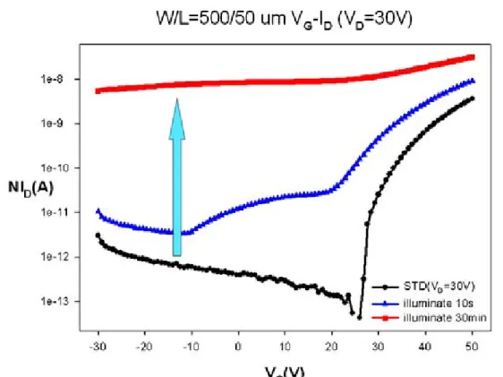
(35) 4.3.2 The steady state of time mode and bias mode Fig. 4.16 and Fig. 4.17 show the ID-VG transfer characteristics of ZnZrO TFTs under time mode and bias mode, respectively. The on-current and threshold voltage of ZnZrO TFTs both were decreased, showing similar trends as the time increasing. The variations in Ion and VT of ZnZrO TFTs under bias mode both were larger than that under the time mode. Fig. 4.18 and Fig. 4.19 show the variations of Ion and VT dependents on time mode and bias mode, respectively and both are reaching to the steady state of ZnZrO TFTs caused by oxygen reacted with the electron. As a result, the steady state was achieved more quickly with bias mode method than that with the Time mode. It also represents the steady state of ZnZrO TFTs under bias mode was accelerated that is a reaction of the adsorbed oxygen atoms with electron.. 4.3.3 The steady state of bias mode after illumination Based on the results described above, the bias mode is come into use for ZnZrO TFTs after illumination. Fig. 4.20 shows transfer characteristics of ZnZrO TFTs under bias mode after 30 second of illumination at atmosphere. The electrical characteristics of ZnZrO TFTs transfer to conductor after illuminating 30s. When the ZnZrO TFTs after illuminating 30 second put the bias mode to use and then can be seen the transformation of drain current as the plot in Fig. 4.21. Consequently, off-current is obviously decreased, because the oxygen molecules capture the electrons causing the reduction of bulk conductivity. But, on-current is not altered after the ZnZrO TFTs performed with bias mode. This indicates that the conductive channel is not influenced by oxygen. When the bias 23.
(36) mode is in used, plenty of the electrons flow in bulk to preclude diffusion of oxygen deep into the conductive channel of the grains [4.5,4.9]. In other word, the oxygen only adsorbs on the ZnZrO surface as negatively charged ion by capturing free electrons due to create a depletion layer that is not influenced to conductive channel. Fig. 4.20 and Fig. 4.22 show the VG-ID transfer characteristics of ZnZrO TFTs under bias mode after illuminating 30 second. It showed similar trends at atmosphere and vacuum. The difference between Fig. 4.20 and Fig. 4.22 is the degree of reduction. The different results will be attributed to the environment effect that the magnitude of oxygen at vacuum is less than at atmosphere. In addition, Fig. 4.23 shows the transformation of drain current under bias mode at vacuum is a decrease of the same degree less than at atmosphere.. 24.
(37) 4.4 The influence of temperature 4.4.1 Experiment In this section, it is separated into two parts to discuss : (1) The influence of temperature under atmosphere. (2) The influence of temperature under vacuum. We set up an experiment to measure I-V characteristics by using a HP4156C semiconductor parameter analyzer. The VD-ID and VG-ID in saturation regime (VD=30V) are measured The oxygen adsorption was studied at four temperatures between room temperature and 125℃. To compare the electrical characteristic of ZnZrO TFTs at atmosphere and at vacuum as the above measurement conditions.. 4.4.2 The influence of temperature under atmosphere Fig. 4.24 shows output characteristics of ZnZrO TFTs at various temperatures from 30℃ to 125℃ under atmosphere. Compare the drain current of 30℃ to 100 ℃, the drain current decreased by several orders of magnitude, but it shows that drain current was increased with increasing voltage ranging from 30V to 50V while the ZnZrO TFTs at 125℃. Compare the plots in Fig 4.25 we found a phenomenon of the VD-ID and VG-ID characteristics are mismatch. It is a contrary result of various temperatures experimental data for VD-ID and VG-ID characteristics at atmosphere. As the result, the VD-ID and VG-ID characteristics of ZnZrO TFTs are a steady state that has measured repeatedly. Besides, Fig. 4.26 and Fig. 4.27 show the VD-ID and VG-ID characteristics of ZnZrO TFTs by first measurement at various temperatures from 30℃ to 125℃ under atmosphere, respectively. However, the VG-ID characteristic of ZnZrO TFT 25.
(38) was improved with increasing temperature but the VD-ID characteristic of ZnZrO TFT showed unlike trend. It indicated that the VD-ID and VG-ID characteristics of ZnZrO TFTs also have mismatch behaviors. In addition, Fig. 4.28 shows output characteristics of ZnZrO TFTs were measured by 5 times at temperature of 125℃ under atmosphere. It shows the VD-ID characteristic of ZnZrO TFTs is a gradual steady state by measuring 5 times. According to above-mentioned, the results indicate oxygen release free electrons in bulk to make the films more conductive while rising temperature. But oxygen is capturing free electrons on the surface due to the conductive decrease while the ZnZrO TFTs is operating. So, the I-V characteristic of ZnZrO TFTs is unstable when the device operates at high temperature.. 4.4.3 The influence of temperature under vacuum Fig. 4.29 and Fig. 4.30 show the VD-ID and VG-ID characteristics of ZnZrO TFTs at various temperatures from 30℃ to 125℃ under vacuum, respectively. Based on the results described above section, we found the VD-ID and VG-ID characteristics of ZnZrO TFTs have matched at vacuum. As result, the VD-ID and VG-ID characteristics of ZnZrO TFTs are a steady state that has measured repeatedly. The electrical characteristic of ZnZrO TFTs was increased by a few orders of magnitude upon temperature increasing. It observes that the magnitude of oxygen in the vacuum is less to influence the characteristic of ZnZrO TFTs. Consquently, to preclude adsorption of oxygen capture free electrons from the film surface while temperature increasing [4.10]. The oxygen of chemisorbed on the ZnZrO film surface was desorbed at various temperature from 30℃ to 125℃. 26.
(39) Chapter 5 Conclusion In this study, adsorption and desorption of oxygen was investigated by carrying out electronic measurements on ZnZrO TFTs with various illuminations, various gas pressures and various temperatures. The results represent the electrical properties of ZnZrO TFTs prepared by the sol-gel process depend strongly on the visible light, ambient oxygen and temperature. The current increased upon illumination and decayed slowly under vacuum as illumination was off. The photoconductivity was due to capture of non-equilibrium holes by the surface oxygen states, remaining an equivalent number of excess electrons in the conduction band. Excess oxygen at the surface acted as an acceptor and removed electrons from the bulk to deplete the grains and increase films resistance. The comparison of temperature effect between atmosphere and vacuum for ZnZrO TFTs has also been discussed in this study. There are two factors resist their influence. The one factor among them is the same, which is that the oxygen of chemisorbed on the ZnZrO film surface was desorbed when temperature increasing. Another factor is that oxygen capture free electrons to form O2- on the surface due to the conductive decrease while the ZnZrO TFTs is operating. This factor is the main reason of the magnitude that oxygen in the vacuum is less to capture free electrons. Besides, from a practical point of view, the observed relation between the photoconductivity and oxygen surface adsorption indicates these ZnZrO TFTs may 27.
(40) be a suitable oxygen sensor working at ambient pressure.. 28.
(41) Reference Chapter 1 [1.1]. H. L. Hartnagel, A. L. Dawar, A. K. Jain, C. Jagadish, “Semiconducting Transparent Thin Films”, pp. 3.. [1.2]. R. Navamathavan, J. H. Lim, D. K. Hwang, B. H. Kim, J. Y. Oh, J.H. Yang, H. S. Kim, S. J. Park, “Thin-Film Transistors Based on ZnO Fabricated by Using Radio-Frequency Magnetron Sputtering,” Journal of the Korean Physical Society, vol. 48, no. 2, pp. 271-274, February 2006.. [1.3]. P. F. Carcia, R. S. McLean, M. H. Reilly, G. Nunes, Jr, “Transparent ZnO thin-film transistor fabricated by rf magnetron sputtering,” Appl. Phys. Lett, vol.82, no. 7,pp. 1117-1119, February 2003. [1.4]. K. Kaiya, K. Omichi, N. Takahashi, T. Nakamura, S. Okamoto, H. Yamamoto, Thin Solid Films, vol.409 , pp.116, 2002.. [1.5]. D. C. Look, D. C. Reynolds, C. W. Litton, R. L. Jones, D. B. Eason, G. Cantwell, Appl. Phys. Lett, vol.81,no. 10,pp. 1830-1832, 2002.. [1.6]. J. F. Muth, R. M. Kolbas, A. K. Sharma, S. Oktyabrsky, J. Narayan, J. Appl. Phys, vol. 85, no. 11, pp. 7884-7887, 1999.. [1.7]. M. J. Alam, D. C. Cameron, J. Vac. Sci. Technol A, vol.19, no. 4, pp. 1642-1646, 2001.. [1.8]. J. H. Lee, P. Lin, J. C. Ho, C. C. Lee, “Chemical solution Deposition of Zn1-xZrxO thin films as active channel layers of 29.
(42) thin-film transistors,” Electrochemical and Solid-State Letters, 9 (4) pp. G117-G120, 2006. [1.9]. K. Nomura, H. Ohta, K. Ueda, T. Kamiya, M. Hirano and H. Hosono, “Thin-Film Transistor Fabricated in Single-Crystalline Transparent Oxide Semiconductor,” Science, vol. 300, no. 5623, pp.1269-1272, May 2003.. [1.10] J. F. Wager, “Transparent Electronics,” Science, vol. 300, no. 5623, pp. 1245-1246, May 2003. [1.11] Y. Ohya, T. Niwa, T. Ban, Y. Takahashi, Jpn. J. Appl. Phys, Part 1 vol. 40, pp. 297, 2001. [1.12] S. Masuda, K. Kitamura, Y. Okumura, S. Miyatake, J. Appl. Phys, Vol. 93, pp. 1624, 2003. [1.13]. J. Nishii, F. M. Hossain, S. Takagi, T. Aita, K. Saikusa, Y. Ohmaki, I. Ohkubo, S. Kishimoto, A. Ohmoto, T. Fukumura, F. Matsukura, Y. Ohno, H. Koinuma, H. Ohno, M. Kawasaki, Jpn. J. Appl. Phys, vol. 42, pp. L347, 2003.. 30.
(43) Chapter 2 [2.1]. H. L. Hartnagel, A. L. Dawar, A. K. Jain, C. Jagadish, “Semiconducting Transparent Thin Films”, pp. 17.. [2.2]. W. T. Pawlewicz, J. B. Mann, W. H. Lowdermilk and Milam, Appl. Phys. Lett, vol. 34, pp. 196, 1979.. [2.3]. R. T. Chen and D. Robinson, Appl. Phys. Lett, vol. 60, pp. 1541, 1992.. [2.4]. B. J. Kellett, A. Gauzzi, J. H. James, B. Dwir, D. Paveuna and F. K. Reinhart, Appl. Phys. Lett, vol.57, pp.2588, 1990.. [2.5]. Yasutaka Takahashi, Masaaki Kanamori, Akiko Kondoh, Hideki Minoura and Yutaka Ohya, “Photoconductivity of Ultrathin Znic Oxide Films”, Jpn. J. Appl. Phys. Vol. 33, pp.6611-6615, 1994.. [2.6]. R. Keezer: J. Appl. Phys 35, pp.1866 (1961).. [2.7]. D. A. Melnick, “Znic Oxide Photoconduction, an Oxygen Adsorption Process”, J. Chem. Phys, vol. 26, no. 5, pp.1136-1146, 1957.. [2.8]. Y. Takahashi, A. Ogiso, R. Tomoda, K. Sugiyama, H. Minoura and M.Tsuili, J. Chem. Soc. Faraday Trans, 178, pp.2563, 1982.. [2.9]. M. F. Ogawa, Y. Natsume, T. Hirayama, H. Sakata, J. Mater. Sci. Lett, 9, pp.1351, (1990).. [2.10]. Y. Natsume, H. Sakata, T. Hirayama, Phys. Stat. Sol. (a) 148, pp.485, (1995). 31.
(44) [2.11] S. Bandyopadhyay, G. K. Paul, R. Roy, S.K. Sen, S. Sen, ”Study of structural and electrical properties of grain-boundary modified ZnO films prepared by sol-gel technique”, Materials Chemistry and Physics, 74, pp.83-91(2002). [2.12] J. W. Orton, M. J. Powell, Rep. Prog. Phys. 43, pp.1263 (1980). [2.13] N.F. Mott, Philos. Mag. 19, pp.835 (1969).. 32.
(45) Chapter 4 [4.1] D. A. Melnick, “Znic Oxide Photoconduction, an Oxygen Adsorption Process”, J. Chem. Phys, vol. 26, no. 5, pp.1136-1146, 1957. [4.2] Q. H. Li, T. Gao, Y. G. Wang and T. H. Wang, “Adsorption and desorption of oxygen probed from ZnO nanowire films by photocurrent measurements”, Appl. Phys. Lett, vol.86, 123117, pp.1-3, 2005. [4.3] Y. Shapira, R. B. McQuistan, and David Lichtman, “Relationship between photodesorption and surface conductivity in ZnO”, Physical Review B, vol. 15, no. 4, 1977. [4.4]. Yasutaka Takahashi, Masaaki Kanamori, Akiko Kondoh, Hideki Minoura and Yutaka Ohya, “Photoconductivity of Ultrathin Znic Oxide Films”, Jpn. J. Appl. Phys. Vol. 33, pp.6611-6615, 1994.. [4.5] S. A. Studenikin, Nickolay Golego, and Michael cocivera, “Carrier mobility and density contributions to photoconductivity transients in polycrystalline ZnO films”, J. Appl. Phys., vol. 87, no. 5, pp.2413-2421, 2000. [4.6] R. Martins, P. Barquinha, A. Pimentel, L. Pereira, E. Fortunato, Phys. Stat.Sol. (a) 202 (9) (2005) R95. [4.7]. H. S. Bae, Seongil Im, “Ultraviolet detecting properties of ZnO-based thin film transistors”, Thin Solid Films, 469-470 (2004) 75-79.. [4.8] P. Barquinha , A. Pimentel, A. Marques, L. Pereira, R. Martins, E. Fortunato, “Effect of UV and visible light radiation on the electrical performances of transparent TFTs based on amorphous indium znic 33.
(46) oxide”, J. Non-Crystalline Solids, 352 (2006) 1756-1760. [4.9]. D. H. Zhang, “Fast photoresponse and the related change of crystallite barriers for ZnO films deposited by RF sputtering”, J. Phys. D: Appl. Phys. 28 (1995) 1273-1277.. [4.10] R. J. Collins and D. G. Thomas, “Photoconduction and Surface Effects with Znic Oxide Crystals”, Physical Review, vol. 12, no. 2, 1958.. 34.
(47) Chapter 1 Table 1.1 Some properties of transparent conducting oxides at room temperature.. Chapter 2 Table 2.1 The characteristics of physisorption and chemisorption.. 35.
(48) Chapter 3 Table 3.1 shows experimental flow chart of sol-gel precursor preparation.. Chapter 4 Table 4.1 shows experimental flow chart of gas pressure in my experiment.. 36.
(49) Chapter 1. Fig. 1.1 Transfer characteristics of ZnO and Zn0.97Zr0.03O based TFTs.. Chap 2. Fig. 2.1 The wurtzite lattice of znic oxide: small circles represent znic atoms, whereas large circles depict oxygen atoms. 37.
(50) Fig. 2.2 The band structure of ZnO.. Fig. 2.3 Lennard-Jones Model of physisorption and chemisorption; (a) physisorption of a molecule, (b) chemisorption, where at d=∞,enough energy has been introduced to dissociate the molecule. 38.
(51) Chap 3. Fig. 3.1 shows a device structure of Zn0.97Zr0.03O-based TFTs.. Fig. 3.2 Microscope、Hot chuck、Probe station 39.
(52) Agilent 4284A. Agilent E5250A(Switch). Agilent 4156C. Agilent 41501B(high power). Fig. 3.3 Agilent 4284A、Agilent 4156C、Agilent E5250A (Switch) Agilent 41501B (high power). Fig. 3.4 Temperature controller. 40.
(53) Fig. 3.5 The TTP-6 Probe Station. 41.
(54) Chapter 4. Fig. 4.1 Transfer characteristics of ZnZrO TFTs is measured repeatedly.. Fig. 4.2 Transfer characteristics of ZnZrO TFTs after illuminating 10 sec and 30 min under atmosphere. 42.
(55) Fig 4.3 Transfer characteristics of ZnZrO TFTs illuminate by 30min and then hold on for 5min, 1hr and 4hr under dark environment at atmosphere.. 43.
(56) Fig. 4.4 The transformation of drain current with illumination at atmosphere.. Fig. 4.5 Physical model of effect of oxygen on the conductance of ZnO and the interaction with light. 44.
(57) Fig. 4.6 Transfer characteristics of ZnZrO TFTs after illuminating 10 sec and 30 min under vacuum.. Fig. 4.7 Transfer characteristics of ZnZrO TFTs illuminate by 30min and hold on for 5min, 1hr and 4hr at dark environment under vacuum. 45.
(58) Fig. 4.8 Transfer characteristics of ZnZrO TFTs under different wavelength of illumination.. 46.
(59) Fig. 4.9 Transfer characteristics of ZnZrO TFTs were exposed to 1torr, 10torr, 100torr and 760torr in nitrogen.. Fig. 4.10 Transfer characteristics of ZnZrO TFTs were exposed to 1torr, 10torr, 100torr and 760torr in air. 47.
(60) Fig. 4.11 Transfer characteristics of ZnZrO TFTs were exposed to 1torr, 10torr, 100torr and 760torr in oxygen.. Fig. 4.12 Transfer characteristics of ZnZrO TFTs were exposed to 1torr, 10torr, 100torr and 760torr in helium. 48.
(61) Fig. 4.13 The value of VT variation with pressure. Compared with nitrogen, air ,oxygen and helium for ZnZrO TFTs.. Fig. 4.14 The value of Ion variation with pressure. Compared with nitrogen, air ,oxygen and helium for ZnZrO TFTs. 49.
(62) (a). (b). Fig. 4.15 Two kinds of measurement modes (a) Time mode (b) Bias mode.. 50.
(63) Fig. 4.16 Transfer characteristics of ZnZrO TFTs under the time mode.. Fig. 4.17 Transfer characteristics of ZnZrO TFTs under the bias mode. 51.
(64) Fig. 4.18 The value of Ion variation with time. Compared with time mode and bias mode for ZnZrO TFTs.. Fig. 4.19 The value of VT variation with time. Compared with time mode and bias mode for ZnZrO TFTs.. 52.
(65) Fig. 4.20 Transfer characteristics of ZnZrO TFTs under bias mode after 30 second of illumination at atmosphere.. Fig. 4.21 The transformation of drain current under bias mode at atmosphere.. 53.
(66) Fig. 4.22 Transfer characteristics of ZnZrO TFTs under bias mode after 30 second of illumination at vacuum.. Fig. 4.23 The transformation of drain current under bias mode at vacuum. 54.
(67) Fig. 4.24 Output characteristics of ZnZrO TFTs at temperatures from 30℃ to 125 ℃ under atmosphere.. Fig. 4.25 Transfer characteristics of ZnZrO TFTs at temperatures from 30℃ to 125℃ under atmosphere. 55.
(68) Fig. 4.26 Output characteristics of ZnZrO TFTs by first measured at temperatures from 30℃ to 125℃ under atmosphere.. Fig. 4.27 Transfer characteristics of ZnZrO TFTs by first measured at temperatures from 30℃ to 125℃ under atmosphere. 56.
(69) Fig. 4.28 Output characteristics of ZnZrO TFTs were measured by 5 times at temperature of 125℃ under atmosphere.. Fig. 4.29 Output characteristics of ZnZrO TFTs at temperatures from 30℃ to 125 ℃ under vacuum. 57.
(70) Fig. 4.30 Transfer characteristics of ZnZrO TFTs by first measurement at temperatures from 30℃ to 125℃ under vacuum.. 58.
(71)
數據
+7
相關文件
Apabila Badan Pelayanan Usaha Swasta Taiwan tidak mendapat surat kuasa dari pihak majikan atau Warga Negara Asing untuk mengurus dan memungut biaya yang tertera pada
Jawaban 1: Majikan harus membeli produk asuransi komersial bagi pekerja migran sebelum kedatangan pekerja migran, dan majikan dari sektor industri (termasuk
*4 Apabila Badan Pelayanan Usaha Swasta Taiwan tidak mendapat surat kuasa dari pihak majikan atau Warga Negara Asing untuk mengurus dan memungut biaya yang tertera pada angka nomor
Berdasarkan hasil analisa uji klinis menunjukkan vaksin ini terhadap orang yang menerima uji coba dari remaja usia genap 16 tahun ke atas dan orang dewasa yang telah
Để giảm thiểu giấy tờ cần kèm theo khi chủ sử dụng lao động xin tuyển dụng lao động, Bộ lao động sẽ căn cứ vào số chứng minh thư và mối quan hệ trên đơn xin và thông qua
dPal dus kyi ’khor lo’i ’grel chen dri ma med pa’i ’od kyi rgya cher bshad pa de kho na nyid snang bar byed pa zhes bya ba. dBu ma la ’jug pa’i
課程ID DEMO_TA00 課程名稱 DEMO_TA00
Direct Access Attack 直接訪問攻擊. 詳細的攻擊手段描述請閱附件一 SQL
