行政院國家科學委員會專題研究計畫 成果報告
砷銻化銦中紅外線材料與元件(2/2)
計畫類別: 個別型計畫 計畫編號: NSC93-2215-E-002-013- 執行期間: 93 年 08 月 01 日至 94 年 10 月 31 日 執行單位: 國立臺灣大學電子工程學研究所 計畫主持人: 林浩雄 計畫參與人員: 蔡濟印 馬大鈞 鄒李昌 報告類型: 完整報告 報告附件: 國際合作計畫研究心得報告 處理方式: 本計畫可公開查詢中 華 民 國 95 年 2 月 4 日
中文摘要
本計畫的目標在於研究三五族中紅外線半導體材料與元件的分子束磊晶成長與特性分 析。我們首先研究 InAsSb/InAs 第二型多層量子井的分子磊晶成長,並分析其結構與光 學特性。藉由溫變光激螢光譜的分析,我們除了比較量子井的特性之外,並分析了 InAsSb/InAs 的能帶排列。我們發現這個合金的導電帶與價電帶都有彎曲效應,其彎曲 參數比為四比六。此外我們並應用此結構製作波長 ~ 4 µm 之多量子井 PIN 發光二極 體。這種發光二極體適合於二氧化碳氣體偵測之用。為了更進一步改善元件中載子的侷 限,我們也研究成長與InAs 接近晶格匹配的 InPSb。InPSb 材料具有 0.64eV 的能隙,但 是位於混熔隙(miscibility gap)之中。我們發現進行接近晶格匹配的成長時,同調應變的 應變能可形成一個局部的亞穩態區,容許單相的磊晶成長。我們成功地完成InPSb 的成 長,並分析其結構與光學特性。這是首次應用分子束磊晶法成長接近 InAs 晶格常數的 InPSb 磊晶層。 關鍵詞:含銻三五族半導體、分子束磊晶、中紅外線光電元件、砷化銦、銻砷化銦、多 量子井、彎曲參數、銻磷化銦、混熔隙、同調應變。ABSTRACT
We report detailed studies of the growth and characterization of InAsSb/InAs multiple quantum wells (MQWs) and InPSb alloy. The InAsSb/InAs MQW samples were grown by molecular beam epitaxy on InAs substrates with the Sb mole fraction ranging from 0.06 to 0.13. From 4K PL, we observed staggered type-II behaviors of the MQWs. By comparing the emission peak energies with a transition energy calculation, we found that both the conduction and valence bands of InAsSb alloy have bowing effect. Their bowing parameters are in the ratio of 4:6. For sample with Sb composition ~0.12, the emission band covers the absorption peak of CO2, and thus a PIN LED with InAsSb/InAs MQW was fabrication. Its
emission wavelength is ~ 4 µm and is suitable for CO2 detector application. The growth of
InPSb on InAs substrates was also investigated. InPSb has a band gap energy of 0.64eV, however, is located at a miscibility gap when it is nearly lattice-match to InAs. In this investigation, we found that the coherent strain energy can form a local meta stable region around the lattice-match composition. Therefore, by carefully optimizing the growth parameters, we successfully grew high quality InPSb bulk layers on InAs substrates. This is the first demonstration of MBE grown single phase InPSb bulk layers on InAs.
Keywords: III-V-Sb semiconductor, molecular beam epitaxy, Mid-Infrared optoelectronic
devices, InAs, InAsSb, multiple quantum well, bowing parameter, InPSb, miscibility gap, coherent growth,.
INTRODUCTION
Among the family of bulk III-V compound semiconductors, InAs1-xSbx alloy system has
the lowest band gap energy (Eg = 0.145 eV at x = 0.634) and is thus an important material for mid-IR devices [1, 2]. Heterostructures based on InAsSb alloy such as InAs/InAsSb, InAsSb/InAsPSb, InAsSb/ InGaSb, and so on, have been widely applied as the active medium for mid-IR optoelectronic devices [3-6]. Among them, InAsSb/InAs quantum well (QW) owns the advantages of much simpler fabrication and lower cost especially for the applications for 3-5 µm light-emitting diodes, which are widely used in gas analyzers and are important for environment protection [6]. In this study, we report the optical properties of a series of InAsSb/InAs multiple quantum wells (MQW’s) grown by molecular beam epitaxy on InAs substrates. Photo- luminescence (PL) measurement was taken to acquire all samples’ band-gap energy and qualitatively compare each sample’s optical characteristics. Transition energies of above mentioned samples are within the range of 0.2~0.4eV (3~5µm).
InPSb is a potential semiconductor alloy for optoelectronic device applications in mid-infrared (2-5µm) wavelength region. Its room temperature band gap covers the range from 1.35 eV (InP) to 0.17 eV (InSb). However, a very large miscibility gap in InPSb alloy extending from x = 0.02 to 0.97 at 480oC was reported in [7-8]. As a result, very limited
efforts were placed on this alloy. So far, only MOCVD has been successfully used to deposit single phase epilayers over the whole composition range [7, 9]. Basically, InP0.69Sb0.31 and its
extended quaternary alloy InAs1-yP0.69ySb0.31y are lattice-matched to InAs and have large
conduction band offset as combined with InAs. Therefore, they may serve as either cladding layer or quantum barrier layer for the optoelectronic devices. Up to now, they have found applications in aluminum-free MIR lasers, emitters and etc. [10-13]. However, almost all the InAs(PSb) materials reported in literatures were grown by MOCVD. In this study, we report InPSb bulk layers grown by GSMBE. To our best knowledge, this work is the first report on MBE-grown InAs lattice-matched InPSb alloy.
EXPERIMENT
The InAsSb/InAs MQW samples were grown on (100) n+-InAs substrates by a VG-V80H MBE system. Two cracking cells were used to provide Sb and As2 beams. A
thermal effusion K-cell was used to provide In flux. An InAs buffer layer with a thickness of 100 nm was grown at 480oC. Then 7-period InAsSb/InAs MQWs with various Sb compositions was grown at 450oC. The thickness of the InAsSb well and InAs barrier are 7 nm and 50 nm, respectively. In-situ reflection high energy electron diffraction (RHEED) was used to monitor surface reconstruction. After the growth, samples were characterized by double crystal X-ray diffraction and photoluminescence (PL) for their structural and optical properties.
A gas-source VG-V80H MBE system was used to grow InPSb bulk samples on InAs substrates. For the growth for substrate effect study, besides the InAs substrates, semi-insulating GaAs and InP substrates were also bonded on the same Moly block. A thermal effusion K-cell was used to provide In flux. P2 beam was cracked from a gas K-cell.
Its flux rate was controlled by the pressure of phosphine (PH3) gas applied into the PBN tube
inside the gas K-cell. Mixed Sb1 and Sb2 beam was provided by an EPI Sb cracking cell. The
substrates were exposed to atomic hydrogen species from an EPI unibulb RF plasma cell to remove the surface oxide. The InPSb bulk layer was then deposited on the cleaned substrates. The growth temperature varied from 420oC to 480oC. In-situ reflection high energy electron diffraction (RHEED) was used to monitor surface reconstruction. After the growth, samples were characterized by BEDE QC2a double crystal X-ray diffraction and Philips PANalytical: X' Pert PRO Powder X-Ray and photoluminescence (PL) for their structural and optical properties.
RESULT AND DISCUSSION
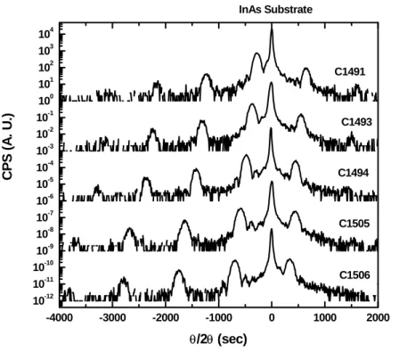
Fig. 1 shows the DXRD spectrums of the InAsSb/InAs MQW samples. During the growth of the MQWs, the in-situ RHEED pattern showed clear 4×2 reconstructions when InAs was deposited, and became slightly blurry when InAsSb was deposited. It implies a rougher growing surface when Sb beam was illuminated. For samples with more Sb composition, only bulk lines were observed, and we believe that it may result from the stress caused by lattice mismatch. However, the satellite peaks in the DXRD spectrums of these samples show only ~80 sec linewidths, indicating their good crystal quality. The Sb compositions of the MQWs in these samples were determined from these measurements. Besides DXRD, PL was performed to examine their optical quality. Fig. 2 shows the low temperature (4K) PL spectrums of the MQW samples. As the Sb composition increases, the peak wavelength has a red shift in the range from 3.4 to 4.5 µm and the peak intensity decreases. From the DXRD measurement, the highest Sb composition in this series is 0.137. A critical thickness
-4000 -3000 -2000 -1000 0 1000 2000 10-12 10-11 10-10 10-9 10-8 10-7 10-6 10-5 10-4 10-3 10-2 10-1 100 101 102 103 104 InAs Substrate C1506 C1505 C1494 C1493 CPS ( A . U. ) θ/2θ (sec) C1491
calculation based on Matthews-Blakeslee model [14] indicates the thickness is 57 nm for the sample with the highest Sb mole fraction. The thickness is much larger than the total InAsSb QW thickness, 35 nm, in the sample. Therefore, the misfit dislocation can not be attributed to the intensity decrement for the samples with more Sb composition. The good crystallinity shown by Fig. 1 also supports this point. Basically, strained InAsSb/InAs MQW on InAs substrate is a staggered type-II heterostructure [15]. The conduction band minimum of InAsSb is higher than that of InAs, and electrons in the samples will mostly stay in the InAs layer. Because the structures in this study have no high barrier layers to confine electrons in the MQW region, the electron population in InAsSb is very low and decreases as Sb composition increases. Since the holes are confined in InAsSb, the samples with higher Sb mole fraction will have lower wavefunction overlap, and therefore, lower dipole matrix element and recombination rate. A simple calculation based on effective mass approximation solving the Schrodinger equation for the electron and hole wave-functions of the flat band structure was made and showed that the intensity ratios between the samples are in the reasonable range. For C1491, two small dips located at 3.43 and 3.52 µm can be observed in Fig. 2. These dips are due to the absorption of methane. And also shown in the figure, a more evident absorption dip at 4.26 µm for sample C1504 is due to carbon dioxide. The QW with a Sb mole fraction of 0.12 is thus suitable for CO2 gas detector.
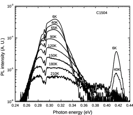
Temperature dependent PL measurements were performed on these samples. Fig. 3 shows a typical result, the spectrums of C1504 with the temperature ranging from 6K to 210K. As the temperature increases, the main emission peak which is from the InAsSb/ InAs MQW has an energy red shift and intensity decrement. The activation energy of the luminescence quenching is 28.5 meV [16]. As can be seen in Fig. 2, the InAsSb/InAs MQWs with lower Sb composition have stronger intensity at 4K. However, the thermal quenching for these samples is faster, and their quenching energies are smaller. Since MQW with higher Sb composition has larger quenching energy, the non-radiative recombination process is likely through a level 15~20 meV below the InAsSb conduction band. As the temperature rises, the electrons in the conduction band edge of the InAs layers are gradually thermalized to the level where the non-radiative recombination process is processed. Besides the main peak, InAs peak located at 0.416 eV is also observed. As can be seen, InAs peak is quickly quenched as temperature rises. On the low energy shoulder, the dual absorption dips attributed to CO2 are clearly
3.0 3.2 3.4 3.6 3.8 4.0 4.2 4.4 4.6 4.8 0 1x10⁻⁴ 2x10⁻⁴ 3x10⁻⁴ 4x10⁻⁴ 5x10⁻⁴ 6x10⁻⁴ C1506 x=0.137 C1504 x=0.12 C1494 x=0.105 C1492 x=0.095 C1493 x=0.085 P L In te n s ity (A .U .) Wavelength(µm) 4.2K PL x5 C1491 x=0.065 InAs1-xSbx/InAs MQW
Fig. 2 4K PL spectrums of InAsSb/InAs MQWs with various Sb
composition.
Fig. 2 4K PL spectrums of InAsSb/InAs MQWs with various Sb
composition. 0.24 0.26 0.28 0.30 0.32 0.34 0.36 0.38 0.40 0.42 0.44 10-6 10-5 10-4 10-3 40K 6K 210K 180K 150K 120K 90K 65K 6K C1504 40K P L i n te n s it y (A. U .)
Photon energy (eV)
Fig. 3 Photoluminescence spectrums of C1504 at different temperatures
ranging from 6K to 210K.
Fig. 3 Photoluminescence spectrums of C1504 at different temperatures
ranging from 6K to 210K. 3.0 3.2 3.4 3.6 3.8 4.0 4.2 4.4 4.6 4.8 0 1x10⁻⁴ 2x10⁻⁴ 3x10⁻⁴ 4x10⁻⁴ 5x10⁻⁴ 6x10⁻⁴ C1506 x=0.137 C1504 x=0.12 C1494 x=0.105 C1492 x=0.095 C1493 x=0.085 P L In te n s ity (A .U .) Wavelength(µm) 4.2K PL x5 C1491 x=0.065 InAs1-xSbx/InAs MQW 0.24 0.26 0.28 0.30 0.32 0.34 0.36 0.38 0.40 0.42 0.44 10-6 10-5 10-4 10-3 40K 6K 210K 180K 150K 120K 90K 65K 6K C1504 40K P L i n te n s it y (A. U .)
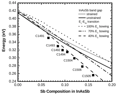
Fig 4 shows the peak energies of the InAsSb/InAs MQWs obtained from the 4K PL measurements as a function of Sb composition. The bulk band gap energies of unstrained InAsSb and compressively strained InAsSb are also plotted in the figure. As can be seen, the energies of the MQWs are lower than that of either unstrained or strained band gap energy. It clearly implies that the band lineup of the heterostructure is type-II. Wei and Zunger [15] have calculated the band lineup of InAsSb alloy. They indicated that the As-rich InAsSb/InAs is type-I when both materials are unstrained and type-II when the InAsSb alloy is compressively strained. We further calculated the transition energy from the electron state in InAs to the heavy-hole state in strained InAsSb. Three curves with different band linups are depicted in the figure. In some reports [15, 17], the band gap bowing in InAsSb alloy is 100% attributed to the conduction band. However, in this case, the calculated data deviate from the experimental results significantly as can be seen in the figure. This finding implies that from our experimental results the conduction band offset is much larger than that predicted in Ref [8]. As shown in the figure, if we lower the conduction band bowing parameter to 40% of the band gap bowing parameter and place the rest 60% to the valence band, the calculated curve
0.00 0.05 0.10 0.15 0.20 0.24 0.26 0.28 0.30 0.32 0.34 0.36 0.38 0.40 0.42 0.44
InAsSb band gap strained unstrained Ec-Ehh transiton 100% EC bowing 70% EC bowing 40% EC bowing C1504 C1506 C1505 C1494 C1493 C1492 Ene rgy (eV) Sb Composition in InAsSb C1491
Fig. 4 Electron to heavy hole transition energy as a function of Sb
is in good agreement with the experimental results. 3.6 3.8 4.0 4.2 4.4 4.6 4.8 5.0 1 2 3 4 5 6 7 8 9 10 11 230K 200K 120K 160K 180K 140K 100K 90K 80K 50K 70K 60K 40K 30K CO2 absorption Wavelength (µm) Inte ns ity (a .u) 4K 10K 20K EL C1547
Fig.6 EL spectrums of PIN InAsSb/InAs
LED at various temperatures ranging from 4K to 230K.
An InAs0.87Sb0.13/GaAs PIN structure was grown on p+-InAs substrate by molecular
beam epitaxy. The structure is shown in Fig. 5. Its active medium is a 7-period InAsSb/GaAs QWs. The sample was sent to Prof. A. Krier’s group at Lacaster University for device fabrication and characterization. The EL spectrums of the LED are shown in Fig. 6. As can be seen, the device shows a clear dip located at 4.2 µm which is due to the absorption of CO2 gas.
The device is thus suitable for the application of carbon dioxide detection. As shown in the figure, the intensity of the LED quenches rapidly as the temperature > 180K. From above discussion, the band alignment of InAsSb/InAs MQW is type-II. Therefore, in this prototype device, the electrons are liable to stay in the thick InAs region and result in intensity quenching. It implies that a carrier confinement layer is needed for higher temperature operation.
X6
p
+-InAs substrate
InAs 1.5 µm
InAs
0.87Sb
0.135 nm
n-InAs 1 µm
InAs 15 nm
InAs
0.87Sb
0.135 nm
X6
p
+-InAs substrate
InAs 1.5 µm
InAs
0.87Sb
0.135 nm
n-InAs 1 µm
InAs 15 nm
InAs
0.87Sb
0.135 nm
p
+-InAs substrate
InAs 1.5 µm
InAs
0.87Sb
0.135 nm
n-InAs 1 µm
InAs 15 nm
InAs
0.87Sb
0.135 nm
Fig.5 Layer structure of PIN InAsSb/InAs
LED. The 7-period InAsSb/InAs MQWs are located in the I layer.
As reported in [7], the binodal points of InP1-xSbx at 450 oC are located at x = 0.02 and
0.96, which means most of the alloy compositions are in the miscibility gap. The critical temperature for InPSb is 1046 oC, slightly lower than the melting point of InP but far above that of InSb. In this situation, non-equilibrim growth technique is needed to overcome the immiscibility. MBE is generally regarded as non-equilibrium or kinetic-controlled process. However, thermodynamics still plays a role in the MBE growth in certain growth conditions, especially when the adatoms have very good migration ability which allows them to find the best place to minimize the free energy. Strongly retarding the migration ability may resolve the immiscibility; however, it would also result in non-radiative centers and deteriorates the optical properties. To make the matter worse is that InPSb contains two group-V elements. Therefore, a trade-off in the growth conditions should be reached to inhibit the phase separation and meet the requirements of composition and quality simultaneously.
The free energy of InPSb GS can be calculated by Stringfellow’s DLP model [18] as
follows, )] x 1 ln( ) x 1 ( x ln x [ RT K GS =− + + − − (1) a02.5
where K is a constant of 1.26×10⁷ cal/mole Ao2.5, a
0 is the lattice constant of the epilayer, and
x is the Sb composition. The spinodal points are just the inflexion points on the curve. Generally, equation (1) does not consider the effect of coherent growth and the related strain energy. However, for the epilayer nearly lattice-match to the substrate, the coherent strain energy will be involved in the reaction and should be included into the free energy GS. Basically, no matter what type of strain is, epilayers with larger lattice mismatch will suffer from the penalty of the strain energy. Therefore, the strain energy is a concave up function of the composition and with its minimum at the point of lattice match. If we take the strain energy into account, the inflexion points will disappear. That means the strain energy prohibits the phase separation. However, for composition with very large mismatch, the epilayer will be easily relaxed or partially relaxed because of its thin critical thickness. In this case, the effect of strain is not pronounced, and the immiscibility still exists. Therefore, strain energy due to coherent growth only provides a very local metastable region centered at the lattice-match composition that can prevent from immiscibility. This phenomenon was first observed when InGaAsP was grown on InP by liquid phase epitaxy [19].
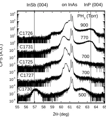
55 56 57 58 59 60 61 62 63 64 65 10-8 10-7 10-6 10-5 10-4 10-3 10-2 10-1 100 101 102 103 104 C P S (A.U .) 2Θ (deg) C1726 C1725 C1727 C1730 C1731 InP (004) InSb (004) on InAs 900 770 700 700 500 PH 3 (Torr)
Fig. 7 Powder XRD results of InPSb bulk grown under different PH3 flow
rates.
different PH3 flow rates. The In/Sb BEP ratio was kept ~2, and the growth rate was 1µm/hr.
When the PH3 pressure is reduced to 500 torr, the epilayer clearly suffers from phase
separation, i.e. it shows an InSb peak and a broader P-rich InPSb peak. In fact, we also grew samples with less PH3 flux rate. In these samples, much clearer phase separation (not shown)
corresponding to the predicted binodal points [7] was observed. These findings suggest that low PH3 flux reduces the incorporation of P and drives the solid composition out of the tiny
metastable region resulted from the strain energy. Therefore, phase separation especially the InSb phase is observed. As the PH3 pressure increases to 700 torr, only one broad epilayer
peak is observed, indicating the growth is taking place in the metastable region. However, the broad peak in fact is composed of several tiny peaks. The tiny peaks could represent different phases or structure of quasi-periodic composition variation in the epilayer. Basically, InPSb is an alloy with two volatile group-V elements. If the free energy of the deposited surface layer can affect the incorporation of Sb or P, it could result in a periodic composition variation. Increase the V/III ratio can reduce the effect of thermo-equilibrium and could prevent from the formation of those tiny peaks. Further increase the PH3 pressure to 770 and 900 torr,
have to reach suitable V/III ratio and P/Sb composition ratio at the same time. Sb flux should be increased so as to reach the lattice-match composition at high V/III ratio.
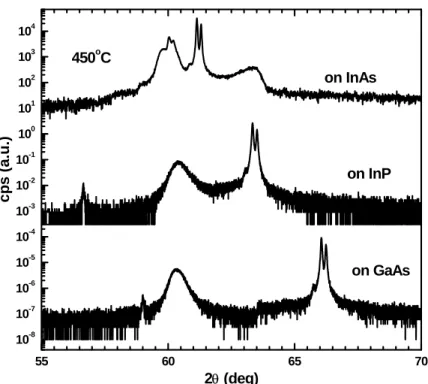
Fig. 8 further elucidates the strain effect. To ensure the same growth condition, we deposited InPSb on InAs, GaAs and InP substrates which were bonded side-by-side on the same moly block. In/Sb BEP ratio which was 1.8 and PH3 pressure was set to 700 torr. The
InPSb grown on InAs substrate shows phase separation but only one phase can be observed in the epilayers grown on InP and GaAs substrates. Since the lattice mismatches between the epilayers and GaAs and InP substrates are too large to sustain coherent growth, the epilayers quickly relax by generating misfit dislocations. As the metamorphic InPSb becomes thick enough, it plays the role of substrate and provides the strain effect to prevent the following strain-free deposition from phase separation. If we assume that the layer deposited on InAs substrate is with the same composition, the growth should be located in the metastable domain. However, slight phase separation is still observed. According to the DLP model, InP has the lowest free energy among the ternary. Therefore, a slight energetic agitation in the metastable domain may cause the formation of InP phase. This finding indicates that it is
55 60 65 70 10-8 10-7 10-6 10-5 10-4 10-3 10-2 10-1 100 101 102 103 104 450oC cp s (a. u .) 2θ (deg) on GaAs on InP on InAs
Fig. 8 Powder XRD results of InPSb grown on different substrates to
easier to obtain single phase InPSb on lattice-mismatch substrate. However, for device application, deposition on lattice-match substrate is definitely necessary.
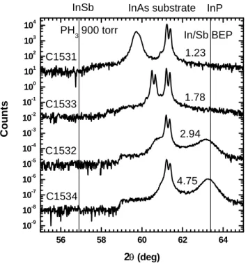
Fig. 9 shows the powder XRD spectrums of InPSb grown on InAs substrates under different In/Sb ratios. The PH3 pressure was set at 900 torr to maintain high V/III ratio growth
condition. As can be seen in the figure, sample C1533 has very pure phase since kα1 and kα2
peaks can be clearly resolved from the epilayer signal. For samples with less Sb flux rate, InP phase can be clearly identified. The compositions of these two samples have been out of the metastable domain and thus phase separations take place in the growth. For samples with higher Sb flux rate, only one broad peak is observed. The growth of this sample may be started in the margin of the metastable domain. Because of the large mismatch, misfit dislocation is generated as the layer thickness exceeds the critical thickness. The relaxed lattice may gradually shift the metastable domain to meet the composition and therefore avoid the phase separation.
56 58 60 62 64 10-9 10-8 10-7 10-6 10-5 10-4 10-3 10-2 10-1 100 101 102 103 104 C1534 C1532 C1533 Co un ts 2θ (deg) C1531 InAs substrate InSb InP 1.23 1.78 2.94 4.75 In/Sb BEP PH 3 900 torr
Fig. 9 Powder XRD spectrums of InPSb grown on InAs substrate under
various In/Sb BEP ratios.
The high resolution XRD spectrums of C1533 are shown in Fig. 10. As can be seen, the epilayer peak in the (004) measurement is with fringing and the linewidth is only ~60 arcsec, close to that of the substrate. (115) measurement is used to confirm the coherent growth of
in the (004) measurement was also analyzed. However, it corresponds to a periodic thickness of ~ 300 nm, which is not consistent to the layer thickness, 1000 nm. Long range composition variation may exist in this sample.
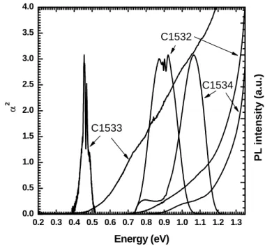
Fig. 11 shows the PL and FTIR results of InPSb epilayers. However, the FTIR measurement was taken on the epilayers grown on GaAs substrates. The PL signal of C1533 has a dip which is due to the absorption of water vapour at 2.73 µm. The PL and absorption spectrums of two other P-rich InPSb layers show slow increase low energy tails, which is attributed to be the result of inhomogeneous composition in the crystal.
-3000 -2000 -1000 0 1000 10-4 10-3 10-2 10-1 100 101 102 103 104 105 106 107 Θ (arcsec) CPS (A . U.) (004) (115) C1533
Fig. 10 High resolution (004) and (115) XRD spectrums of InPSb
sample C1533. 0.2 0.3 0.4 0.5 0.6 0.7 0.8 0.9 1.0 1.1 1.2 1.3 0.0 0.5 1.0 1.5 2.0 2.5 3.0 3.5 4.0 α 2 Energy (eV) C1533 C1532 C1534 PL inte n s ity (a .u .)
CONCLUSIONS
We have investigated the growth and photoluminescence of InAsSb/InAs MQW structures. Staggered type-II behaviors in the MQWs are observed. By comparing the 4K emission peaks of the MQW with a calculation for the electron to heavy-hole transition energy, we found that the band gap bowing is not totally attributed to the conduction band. The bowing parameters of the conduction and valence bands are 40% and 60% of that of the band gap. For Sb composition ~0.12, the emission band covers the absorption energy of CO2 gas and is very
suitable for CO2 gas detector application. The growth condition of InPSb lattice matched to
InAs substrate was also investigated. Influence of growth conditions and the strain effect due to substrate are discussed. By carefully optimizing the growth condition, good crystal quality InPSb bulk can be grown on InAs substrate by gas source MBE without phase separation.
REFERENCES
[1] G. C. Osbourn, "InAsSb strained-layer superlattices for long wavelength detector applications," J. Vac. Sci. Technol. B 2, 176 (1984).
[2] Z. M. Fang, K. Y. Ma, D. H. Jaw, R. M. Cohen, and G. B. Stringfellow, "Photoluminescence of InSb, InAs, and InAsSb grown by organometallic vapor phase epitaxy," J. Appl. Phys. 67, pp.7034 (1990).
[3] Y. H. Zhang, "InAs-InAsxSb1-x type-II superlattice midwave infrared lasers grown on
InAs substrates," IEEE J. Sel. Topics in Quantum Electron., 1, 749 (1995).
[4] B. Lane, D. Wu, A. Rybaltowshi, H. Yi, J. Diaz, and M. Razeghi, "Compressively strained multiple quantum well InAsSb lasers emitting at 3.6 µm by metal-organic chemical vapor deposition," Appl Phys. Lett., 70, 443 (1997).
[5] A. A. Allerman, R. M. Biefeld, and S. R. Kurtz, "InAsSb-based mid-infrared lasers (3.8-3.9 mm) and light- emitting diodes with AlAsSb claddings and semimetal electron injection, grown by metalorganic chemical vapor deposition," Appl. Phys. Lett., 69, 465 (1996).
[6] N. V. Zotova, S. S. Kizhaev, S. S. Molchanov, T. B. Popova, and Yu. P. Yakovlev, "Long-wavelength light-emitting diodes (λ=3.4-3.9 µm) based on InAsSb/InAs heterostructures grown by vapor-phase epitaxy," Semiconductors, 34, 1402 (2000).
[7] M. J. Jou, Y. T. Cherng, and G. B. Stringfellow,"Organometallic vapor-phase epitaxtial growth and characterization of the metastable alloy InP1−xSbx," J. of Applied Physics, 64,
1472 (1988).
[8] K. Onabe, " Unstable Regions in Type ABCD III-V Quaternary Solid Solutions Calculated with Strictly Regular Solution Approximation," Jpn. J. of Applied Physics, Vol. 22, No. 2, pp. 287 (1983)
[9] R. M. Biefeld, K. C. Baucom, S. R. Kurtz and D. M. Follstaedt, "The growth of InP1−xSbx by metalorganic chemical vapor deposition,"J. of Crystal Growth 133, 38
(1993).
[10] A. Joullie, E. M. Skouri, M. Garcia, P. Grech, A. Wilk, P. Christol, A. N. Baranov, A. Behres, J. Kluth, A. Stein, K. Heime, M. Heuken, S. Rushworth, E. Hulicius and T. Simecek, "InAs(PSb)-based “W” quantum well laser diodes emitting near 3.3 µm," Appl.
Phys.Lett., 76, 2499 (2000).
Materials, 29, 91 (2000).
[12] S. R. Kurtz, R. M. Biefeld, A. A. Allerman, A. J. Howard, M. H. Crawford, and M. W. Pelczynski, "Pseudomorphic InAsSb multiple quantum well injection laser emitting at 3.5 µm,"Appl. Phys.Lett., 68, 1332 (1996).
[13] B. Lane, D. Wu, A. Rybaltowshi, H. Yi, J. Diaz, and M. Razeghi, "Compressively strained multiple quantum well InAsSb lasers emitting at 3.6 µm by metal-organic chemical vapor deposition," Appl Phys. Lett., 70, 443 (1997).
[14] J. W. Matthews and A. E. Blakeslee, "Defects in epitaxial multilayers, " J. Crystal
Growth, 27, 118 (1974).
[15] S. H. Wei and A. Zunger, "InAsSb/InAs: a type-I or a type-II band alignment," Phys. Rev.
B, 52, 12039 (1995).
[16] J. I. Pankove, Optical processes in semiconductors, Dover Publications, Inc., New York, 165 (1971).
[17] S. Tiwari and D. J. Frank, "Empirical fit to band discontinuities and barrier heights in III-V alloy systems," Appl. Phys. Lett. 60, 630 (1992).
[18] G. B. Stringfellow, "Calculation of ternary and quaternary III-V phase diagram," J.
Crystal Growth. 27, 21 (1974).
[19] M. Quillec, C. Daguet, J. L. Benchimol, and H. Launois, " InxGa1−xAsyP1−y alloy
stabilization by InP substrate inside an unstable region in liquid phase epitaxy," Appl
Phys. Lett., 40, 325 (1982).