Effect of surface free energy in gate dielectric in pentacene thin-film transistors
Wei-Yang Chou,a兲Chia-Wei Kuo, Horng-Long Cheng, Yi-Ren Chen, and Fu-Ching Tang Institute of Electro-Optical Science and Engineering, National Cheng Kung University, Tainan 701, Taiwan and Department of Physics, National Cheng Kung University, Tainan 701, Taiwan
Feng-Yu Yang, Dun-Yin Shu, and Chi-Chang Liao
Material and Chemical Research Laboratories, Industrial Technology Research Institute, Hsinchu 310, Taiwan and Electronics and Optoelectronics Research Laboratories, Industrial Technology Research Institute, Hsinchu 310, Taiwan
共Received 16 April 2006; accepted 24 July 2006; published online 15 September 2006兲
The surface free energy of a dielectric has a strong influence on the performance of pentacene thin-film transistors. Research shows that by matching surface free energy in the interface of the dielectric and the orthorhombic thin-film phase of pentacene film, the field-effect mobility of transistors is enhanced reaching above 2.0 cm2/ V s. The authors suggested that a more complete first monolayer of pentacene was formed upon the gate dielectric surface with almost identical surface free energy, benefiting carrier transportation. The research also discusses the mechanism of surface free energy effects on the crystalline size and structural disorder in pentacene film. © 2006 American Institute of Physics. 关DOI:10.1063/1.2354426兴
Recent research trends draw much attention to organic semiconductor-based thin-film transistors共TFTs兲 due to dra- matic performance improvements observed in this techno- logical domain. Pentacene-based TFTs represent particular interest as one of the most promising technologies.1,2 The performance of organic TFTs共OTFTs兲 depends on the use of semiconductors and dielectrics. Surface properties, i.e., sur- face energy and surface roughness, of a dielectric layer rep- resent distinctive factors which determine potential improve- ments in electric characteristics of OTFTs.3–5In cases where pentacene is grown upon dielectrics with surface-induced morphology, the structure of the first few monolayers is ex- pected to have a strong impact on mobility.4,6At the same time, it is possible to improve performance by manipulating charge transport qualities in aforementioned devices. It is therefore important to establish precise interfacial control be- tween organic semiconductors/dielectrics in order to achieve higher performance in OTFTs.
Most studies on OTFTs utilize inorganic silicon dioxide 共SiO2兲 as the gate dielectric layer. Typically, the mobility of pentacene-based TFTs featuring SiO2 dielectric is around 0.01⬃0.5 cm2/ V s.1,7,8Researchers indicate that a modifica- tion layer, such as octadecyltrichlorosilane, placed between the SiO2gate dielectric and the pentacene active layer is an effective method allowing to achieve mobility above 1.0 cm2/ V s.7,8The greatest research effort, by far, has been focused on the polymeric materials that have been used as a surface modification layer and/or dielectric layer in OTFTs.9 For instance, Kelley et al. have reported high performance pentacene TFTs using polymeric ultrathin films as a surface modification with mobility above 5.0 cm2/ V s.9 In the re- port, researchers did not observe direct correlation between the surface morphology and resulting mobility. It is widely believed that the carrier transport efficiency is increased through the presence of well-ordered crystalline structure and/or the large grain size. At the same time, some of the
reported data are not consistent with the observations above.10–12
Previously, we have addressed surface-induced orienta- tion of a pentacene film with electrical anisotropic properties using photoalignment polyimide method.13In this study, we have used a photosensitive polyimide共PSPI兲 that served as a modification layer upon SiO2. We have learned that enhance- ment of mobility was a combination of three related factors including the surface free energy of PSPI, the crystalline size, and the disorder of the pentacene film. Surface proper- ties of PSPI can be managed by using photopolymer surface- modifying coating and polarized ultraviolet light exposure.
The technique above allows reaching the required nonpolar- ity that is needed to enhance field-effect mobility of penta- cene TFTs. In the research, we also discuss possible origin of higher mobility in pentacene TFTs with PSPI modifications as compared to mobility observed in bare SiO2.
The device geometry and the sample fabrication were described previously and shown in Figs. 1共a兲 and 1共b兲.13 Fabricated OTFT devices had a channel with a length of 120m and a width of 1920m. As shown in Fig. 1共a兲, a 100 nm PSPI 共EA8001, Eternal Company兲 modification layer was deposited by spin coating directly onto a SiO2 substrate. PSPI was irradiated with polarized ultraviolet 共UV兲 beam with energy of 1 J to form the modification layer.
Obtained modification layer featured the best in-plane aniso- tropic homogeneous liquid crystal 共LC兲 alignment in a LC test cell 共not show herein兲 used for the growth of 70 nm thick pentacene film. The electrical characteristics of TFTs were measured using a Keithley 4200-SCS semiconductor parameter analyzer in a dark chamber.
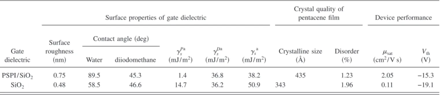
Several publications state that roughness of the gate di- electric has a distinct influence on the morphology and struc- tural properties of pentacene films.3,4Films grown on smooth thermal oxide are generally more ordered and have a larger grain size. Table I presents surface roughness of the PSPI and SiO2 dielectrics measured by atomic force microscope. We can see that the root-mean-square roughness共rms兲 of SiO2 a兲Electronic mail: [email protected]
APPLIED PHYSICS LETTERS 89, 112126共2006兲
0003-6951/2006/89共11兲/112126/3/$23.00 89, 112126-1 © 2006 American Institute of Physics
Downloaded 26 Oct 2008 to 140.116.208.46. Redistribution subject to AIP license or copyright; see http://apl.aip.org/apl/copyright.jsp
surface is superior to the rms of the PSPI surface. The mor- phology of the pentacene thin films on PSPI and SiO2 is shown in Figs. 1共c兲 and 1共d兲, respectively. The grain size of both samples is very similar, even though the PSPI dielectric has inferior roughness compared to the SiO2dielectric. This result is different from the previously reported analyses.3,4 X-ray diffraction共XRD兲 spectroscopy was performed on the pentacene films to make an in-depth study of the differences in crystal structure between pentacene films grown on PSPI and SiO2 surfaces. The XRD patterns of the pentacene de- posited on the experimental gate dielectrics had five distinc- tively explicit reflections 共00l兲, including thin-film phase 共00l兲 and triclinic bulk phase 共00l
⬘
兲, as shown in Fig. 2.Triclinic bulk phase was much weaker as compared to the thin-film phase observed in pentacene grown on the PSPI surface. Observations suggest that the pentacene grown on the PSPI surface has a better crystalline quality as compared to that grown on the SiO2surface. Crystalline parameters of the pentacene films, prepared on PSPI and SiO2 surfaces, were evaluated from paracrystal theory.14 The investigated parameters included the size of the crystalline domain L¯ 关the mean dimension of the crystallites perpendicular to thehkl
plane 共hkl兲兴 and the degree of structural disorder gII 关the distance fluctuation between successive planes of the family 共hkl兲 or second kind of distortions of crystal structure兴. The calculated L¯
hkl and gII values are shown in Table I. Our re-
sults indicate that the ordering of pentacene molecules in- creases significantly on the PSPI surface even if the surface has inferior rms roughness.
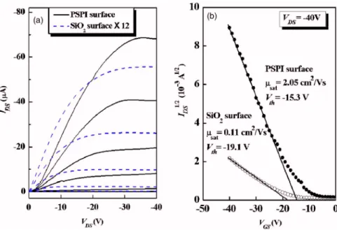
Figure 3共a兲 shows the output characteristics 共IDS-VDS兲 of TFTs produced with pentacene films deposited on the PSPI and SiO2gate dielectrics. The magnitude of IDSproduced by the devices with PSPI layer was significantly larger than that of the devices only with SiO2dielectric. Figure 3共b兲 shows a plot of the square root of IDSas a function of VGSfor OTFTs with PSPI and SiO2 gate dielectrics. Saturation field-effect mobilitysatand threshold voltage Vthare measured for the OTFTs with the PSPI/SiO2dual layer and native SiO2layer by fitting the linear region between −20 and −40 V of VGS and are listed in Table I. As we can see, insertion of the photosensitive layer into the OTFTs resulted in a drastic en- hancement in the field-effect mobility and slight decrease of the threshold voltage.
To understand the mechanism driving the enhancement of the field-effect mobility, the contact angles共FACE contact- angle meter, Kyowa Kaimenkagaku Co.兲 of two test liquids were measured. Water and di-iodomethane represented the test liquids measured on the surfaces of PSPI and SiO2. The contact angles of the test liquids are shown in Table I. Higher contact angle of the water on the PSPI indicates that PSPI’s exposure to an appropriate dose of UV light makes the sur- face of the gate dielectric more nonpolar. Surface free ener- gies of the PSPI and SiO2 dielectrics obtained in the experi- ment are listed in Table I.15 Decrease in the surface free energy on the surface of the PSPI dielectric significantly con- tributes to enhance mobility in OTFTs and consequently
FIG. 1.共Color online兲 Cross section of OTFTs 共a兲 with PSPI layer and 共b兲 without PSPI layer. Atomic force microscope images of pentacene films deposited on共a兲 PSPI and 共b兲 SiO2dielectrics. Two images are 2⫻2m2 in size.
TABLE I. Surface properties of gate dielectrics, crystal quality of pentacene films, and the electrical performance of the corresponding pentacene-based OTFTs.
Gate dielectric
Surface properties of gate dielectric
Crystal quality of
pentacene film Device performance
Surface roughness
共nm兲
Contact angle共deg兲
␥s Pa
共mJ/m2兲 ␥s Da
共mJ/m2兲 ␥sa
共mJ/m2兲
Crystalline size 共Å兲
Disorder
共%兲 sat
共cm2/ V s兲 Vth 共V兲 Water diiodomethane
PSPI / SiO2 0.75 89.5 45.3 1.4 36.8 38.2 435 1.23 2.05 −15.3
SiO2 0.48 58.5 46.6 14.7 36.2 50.9 343 1.96 0.11 −19.1
a␥sis solid surface free energy, and␥s Pand␥s
Dare the polar and dispersion force components of solid surface free energy, respectively.
FIG. 2. 共Color online兲 X-ray spectra of pentacene films grown on PSPI 共solid line兲 and SiO2共dash line兲 dielectrics.
112126-2 Chou et al. Appl. Phys. Lett. 89, 112126共2006兲
Downloaded 26 Oct 2008 to 140.116.208.46. Redistribution subject to AIP license or copyright; see http://apl.aip.org/apl/copyright.jsp
slightly decreases the threshold voltage, as discussed below.
Recently, a thickness driven orthorhombic thin-film phase to triclinic bulk phase transformation is suggested in pentacene thin films.16 In our study, the orthorhombic thin- film phase crystal structure was grown at low film thickness.
As increasing the thickness of pentacene until a critical thickness共⬃30 nm兲 is reached, the triclinic phase starts to form. The surface free energy values were 38 mJ/ m2 for orthorhombic phase and 76 mJ/ m2 for triclinic phase.16 In- terestingly, the surface free energy of PSPI in this study matched the energy of the pentacene orthorhombic thin-film phase. However, the surface free energy of SiO2significantly deviated from the value recorded in orthorhombic thin-film phase. Thus, pentacene grown on low surface energy PSPI layer retains the first pentacene layer better and keeps it from some voids and successive incomplete layers over the first case, which limits the transport of carriers near the gate di- electric, consequently resulting in high carrier mobility.
These conditions are determinant factor behind large crystal- line size and low structural disorder in pentacene film grown on PSPI 共see Table I兲. On the other hand, several publica- tions refer to reduction in mobility due to increased surface roughness of the gate dielectric.3,4,12 However, in our case, PSPI has inferior rms roughness and the morphology of the pentacene films grown on these gate dielectrics is rather similar, despite the fact that the surface free energy is differ- ent. Yang et al.5 have reported that the average grain size becomes smaller as the surface free energy of gate dielectrics decreases which are different from our experimental results.
Hence, we can exclude the assumptions suggesting that per- formance of OTFTs is influenced by the surface morphology of the pentacene film and surface roughness in different types of gate dielectrics. In fact, the surface free energy of the PSPI can be manipulated by regulating the dose of UV light exposure. Initially, we came to the conclusion above when the surface energy for the PSPI measured 38 mJ/ m2 thus matching the surface free energy of the orthorhombic phase pentacene and resulting in optimized performance in OTFTs. Further investigation of the mechanism for changing surface free energy in PSPI is underway.
During the experiment we have fabricated high perfor- mance pentacene-based OTFTs using the PSPI as a modifi- cation layer on gate dielectric. The maximum saturation field-effect mobility was above 2.0 cm2/ V s. We believe that a gate dielectric with low surface free energy can contribute to enhance carrier mobility in pentacene OTFTs, increase crystalline size, and decrease crystal disorder in pentacene films.
The authors would like to thank Eternal Technology Corp. for providing the photosensitive polyimide, the Na- tional Science Council of Taiwan of the Republic of China for financially supporting this research under Contract No.
NSC 94-2112-M-006-022 and NSC 94-2112-M-006-021, and the Center for Micro/Nano Science and Technology Re- search, National Cheng Kung University, Taiwan, for their equipment support and cooperation.
1C. D. Dimitrakopoulos and P. R. L. Malenfant, Adv. Mater.共Weinheim, Ger.兲 14, 99 共2002兲.
2T. W. Kelly, P. F. Baude, C. Gerlach, D. E. Ender, D. Muyres, M. A.
Haase, D. E. Vogel, and S. D. Theiss, Chem. Mater. 16, 4413共2004兲.
3S. Steudel, S. De Vusser, S. De Jonqe, D. Janssen, S. Verlaak, J. Genoe, and P. Heremans, Appl. Phys. Lett. 88, 072109共2004兲.
4S. E. Fritz, T. W. Kelly, and C. D. Frisbie, J. Phys. Chem. B 109, 10574 共2005兲.
5S. Y. Yang, K. Shin, and C. E. Park, Adv. Funct. Mater. 15, 1806共2005兲.
6A. Dodabalapur, L. Torsi, and H. E. Katz, Science 268, 270共1995兲.
7Y.-Y. Lin, D. J. Gundlach, S. F. Nelson, and T. N. Jackson, IEEE Trans.
Electron Devices 44, 1325共1997兲.
8M. Shtein, J. Mapel, J. B. Benziger, and S. R. Forrest, Appl. Phys. Lett.
81, 268共2002兲.
9T. W. Kelley, D. V. Muyres, P. F. Baude, T. P. Smith, and T. D. Jones, Mater. Res. Soc. Symp. Proc. 771, 169共2003兲.
10D. Knipp, R. A. Street, A. Völkel, and J. Ho, J. Appl. Phys. 93, 347 共2003兲.
11L. Torsi, A. Dodabalapur, L. J. Rothberg, A. W. P. Fung, and H. E. Katz, Science 272, 1462共1996兲.
12M. H. Choo, J. H. Kim, and S. Im, Appl. Phys. Lett. 81, 4640共2002兲.
13W. Y. Chou and H. L. Cheng, Adv. Funct. Mater. 14, 811共2004兲.
14D. Dimitrakopoulos, A. R. Brown, and A. Pomp, J. Appl. Phys. 80, 2501 共1996兲, and references therein.
15J. Kinloch, Adhesion and Adhesives共Chapman and Hall, London, 1987兲, Chap. 2, pp. 18-51.
16L. F. Drummy and D. C. Martin, Adv. Mater.共Weinheim, Ger.兲 17, 903 共2005兲.
FIG. 3.共Color online兲 共a兲 Output char- acteristics of the pentacene OTFTs with a PSPI/SiO2 dual-layer gate di- electric共solid line兲 and a SiO2gate di- electric, respectively.共b兲 The saturated transfer characteristics 共IDS1/2-VGS兲 of pentacene OTFTs at VDS= −40 V.
112126-3 Chou et al. Appl. Phys. Lett. 89, 112126共2006兲
Downloaded 26 Oct 2008 to 140.116.208.46. Redistribution subject to AIP license or copyright; see http://apl.aip.org/apl/copyright.jsp