GaN has attracted great interest in the application of optoelec- tronic devices such as light-emitting diodes, laser diodes, UV detec- tors, microwave power devices such as thyristors, and metal-oxide- semiconductor-field-effect transistors.1,2 To achieve high-quality performance of the devices, low-resistance ohmic contacts are es- sential. For p-GaN it is difficult to form the ohmic contacts with a low contact resistance because of the difficulty of obtaining high hole concentrations in p-GaN. Recently, it was reported that anneal- ing in an oxygen-containing ambient allows the Au/Ni bilayer to form ohmic contacts on p-GaN with the contact resistance as low as 10−6⍀ cm2.3-7Several mechanisms were proposed to rationalize the formation of oxidized Au/Ni ohmic contacts on p-GaN. For ex- ample, the formation of a thin p-NiO layer in contact with p-GaN can remarkably reduce the Schottky barrier height.3,5However, the structure of Au/sputtered NiO/p-GaN did not show ohmic behavior.4,6Hydrogen atoms bonded with Mg atoms react with oxy- gen to form H2O, leading to the increase of hole concentrations in the surface of p-GaN.8,9The formation of Ga-Ni compounds at the interface between Ni and GaN are important for forming the ohmic contact.5,10Before deposition of the metal contact preoxidation of p-GaN results in the formation of GaO on the GaN surface, produc- ing Ga vacancies below the metal contact after removal of GaO and thus improving the ohmic contact.7The oxygen atoms incorporated in the Au/Ni bilayer during annealing promote outdiffusion of Ga atoms into the interfacial layer to form GaOx, producing Ga vacan- cies, and thus increasing the hole concentrations.11
These mechanisms illustrated in the aforementioned still need to be clarified. Koide et al.8found that layer reversal occurred in the M共M = Ni, Co, and Cu兲/Au contacts to p-GaN after annealing in oxygen-containing ambient, forming the transition metal oxides on the Au layer. The layer reversal effect may remove the contamina- tion layer on the GaN surface. The oxidized Ni/Au contacts to p-GaN have shown a very low contact resistance. In the present study, therefore, the interfacial reactions and properties of the oxi- dized Au/Cu, Cu/Au, Au/Co, and Co/Au contacts to p-GaN were explored to elucidate the mechanisms responsible for the formation of oxidized ohmic contacts to p-GaN. The results showed that the formation of oxidized Au/Cu and Cu/Au ohmic contacts to p-GaN could be ascribed to the removal of carbon contamination on the GaN surface and formation of Ga vacancies in the GaN surface due to the favored outdiffusion of Ga atoms, both of which are promoted by formation of CuO.
Experimental
The epitaxial Mg-doped GaN films, 2.1m thick, were grown on 共0001兲 sapphire at 1000°C by metallorganic chemical vapor deposition 共CVD兲. The as-grown GaN films were annealed at 750°C in N2to activate the Mg dopants. The carrier concentration is in the range of 1-6⫻ 1017/cm3 by Hall measurement. Before deposition, the GaN films were cleaned with organic solvents and HCl:H2O 共1:1兲 solution successively, and then immersed in a KOH 共45%兲 solution at 75°C for 0.5 h. Carbon and oxide contaminants on the GaN surface can be effectively removed by immersion in the KOH solution.11,13The contact regions with a dimensions of 50⫻ 50 m2 were patterned by the conven- tional photolithography lift-off method. Au共30 nm兲/Cu 共10 nm兲, Cu共10 nm兲/Au 共30 nm兲, Au 共30 nm兲, Au 共30 nm兲/Co 共10 nm兲, and Co共10 nm兲/Au 共30 nm兲 bilayers were deposited on p-GaN in an electron gun deposition system, and then annealed at 400- 500°C for 10 min in N2and air, respectively. The specific contact resistance was measured using the transmission line method共TLM兲.
Phase identification was performed using X-ray diffraction共XRD兲.
Thedepth profiles of chemical elements in the samples were ana- lyzed using Auger electron spectrometry共AES兲 and secondary ion mass spectrometry共SIMS兲, respectively. The chemical states of Ga
*Electrochemical Society Active Member.
zE-mail: [email protected]
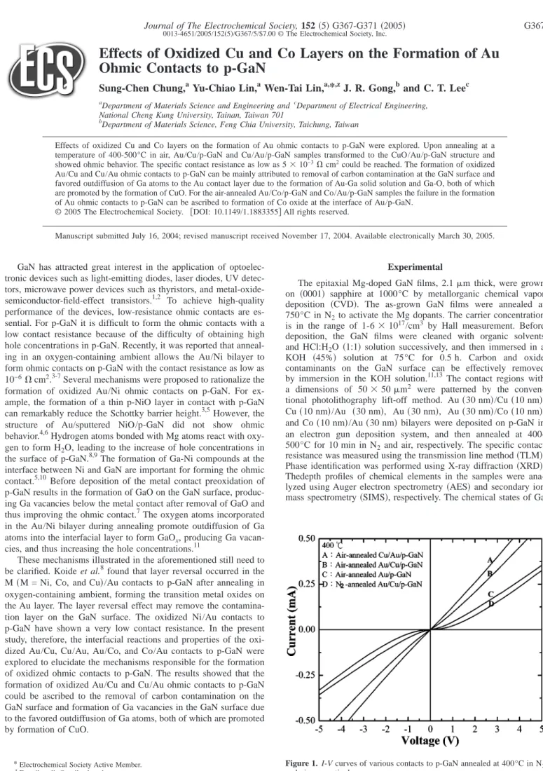
Figure 1. I-V curves of various contacts to p-GaN annealed at 400°C in N2
and air, respectively.
at the interface of Au/p-GaN for air-annealed Au/Cu/p-GaN and Cu/Au/p-GaN samples were measured using X-ray photoelectron spectroscopy共XPS兲.
Results and Discussion
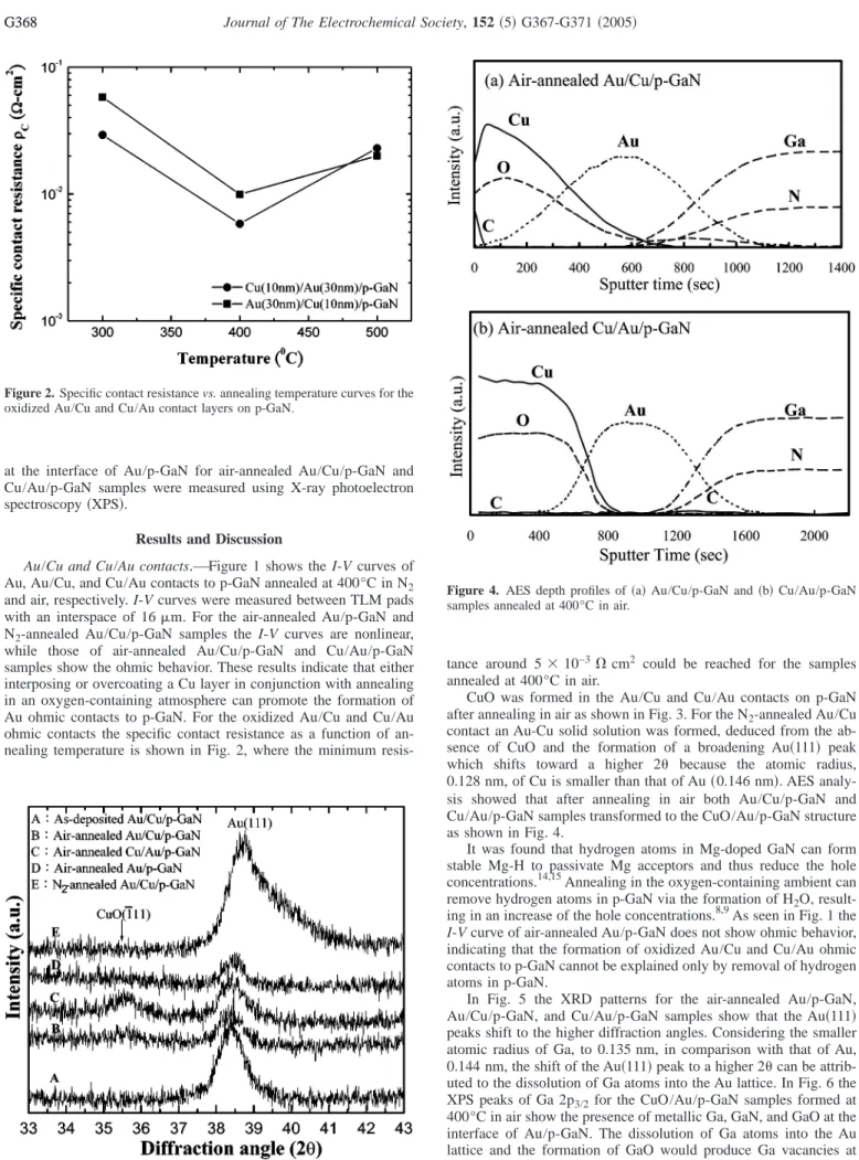
Au/Cu and Cu/Au contacts.—Figure 1 shows the I-V curves of Au, Au/Cu, and Cu/Au contacts to p-GaN annealed at 400°C in N2 and air, respectively. I-V curves were measured between TLM pads with an interspace of 16m. For the air-annealed Au/p-GaN and N2-annealed Au/Cu/p-GaN samples the I-V curves are nonlinear, while those of air-annealed Au/Cu/p-GaN and Cu/Au/p-GaN samples show the ohmic behavior. These results indicate that either interposing or overcoating a Cu layer in conjunction with annealing in an oxygen-containing atmosphere can promote the formation of Au ohmic contacts to p-GaN. For the oxidized Au/Cu and Cu/Au ohmic contacts the specific contact resistance as a function of an- nealing temperature is shown in Fig. 2, where the minimum resis-
tance around 5⫻ 10−3⍀ cm2 could be reached for the samples annealed at 400°C in air.
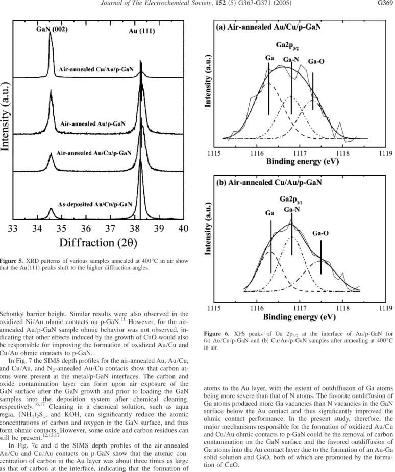
CuO was formed in the Au/Cu and Cu/Au contacts on p-GaN after annealing in air as shown in Fig. 3. For the N2-annealed Au/Cu contact an Au-Cu solid solution was formed, deduced from the ab- sence of CuO and the formation of a broadening Au共111兲 peak which shifts toward a higher 2 because the atomic radius, 0.128 nm, of Cu is smaller than that of Au共0.146 nm兲. AES analy- sis showed that after annealing in air both Au/Cu/p-GaN and Cu/Au/p-GaN samples transformed to the CuO/Au/p-GaN structure as shown in Fig. 4.
It was found that hydrogen atoms in Mg-doped GaN can form stable Mg-H to passivate Mg acceptors and thus reduce the hole concentrations.14,15Annealing in the oxygen-containing ambient can remove hydrogen atoms in p-GaN via the formation of H2O, result- ing in an increase of the hole concentrations.8,9As seen in Fig. 1 the I-V curve of air-annealed Au/p-GaN does not show ohmic behavior, indicating that the formation of oxidized Au/Cu and Cu/Au ohmic contacts to p-GaN cannot be explained only by removal of hydrogen atoms in p-GaN.
In Fig. 5 the XRD patterns for the air-annealed Au/p-GaN, Au/Cu/p-GaN, and Cu/Au/p-GaN samples show that the Au共111兲 peaks shift to the higher diffraction angles. Considering the smaller atomic radius of Ga, to 0.135 nm, in comparison with that of Au, 0.144 nm, the shift of the Au共111兲 peak to a higher 2 can be attrib- uted to the dissolution of Ga atoms into the Au lattice. In Fig. 6 the XPS peaks of Ga 2p3/2for the CuO/Au/p-GaN samples formed at 400°C in air show the presence of metallic Ga, GaN, and GaO at the interface of Au/p-GaN. The dissolution of Ga atoms into the Au lattice and the formation of GaO would produce Ga vacancies at the GaN surface below the Au layer and thus improve the ohmic behavior because Ga vacancies act as acceptors for electrons in GaN. Meanwhile, the formation of GaO would increase the Figure 2. Specific contact resistance vs. annealing temperature curves for the
oxidized Au/Cu and Cu/Au contact layers on p-GaN.
Figure 3. XRD patterns of various contacts to p-GaN annealed at 400°C in N2and air, respectively.
Figure 4. AES depth profiles of共a兲 Au/Cu/p-GaN and 共b兲 Cu/Au/p-GaN samples annealed at 400°C in air.
G368 Journal of The Electrochemical Society, 152共5兲 G367-G371 共2005兲 G368
Schottky barrier height. Similar results were also observed in the oxidized Ni/Au ohmic contacts on p-GaN.11 However, for the air- annealed Au/p-GaN sample ohmic behavior was not observed, in- dicating that other effects induced by the growth of CuO would also be responsible for improving the formation of oxidized Au/Cu and Cu/Au ohmic contacts to p-GaN.
In Fig. 7 the SIMS depth profiles for the air-annealed Au, Au/Cu, and Cu/Au, and N2-annealed Au/Cu contacts show that carbon at- oms were present at the metal/p-GaN interfaces. The carbon and oxide contamination layer can form upon air exposure of the GaN surface after the GaN growth and prior to loading the GaN samples into the deposition system after chemical cleaning, respectively.16,17 Cleaning in a chemical solution, such as aqua regia, 共NH4兲2Sx, and KOH, can significantly reduce the atomic concentrations of carbon and oxygen in the GaN surface, and thus form ohmic contacts. However, some oxide and carbon residues can still be present.12,13,17
In Fig. 7c and d the SIMS depth profiles of the air-annealed Au/Cu and Cu/Au contacts on p-GaN show that the atomic con- centration of carbon in the Au layer was about three times as large as that of carbon at the interface, indicating that the formation of CuO can promote the outdiffusion of carbon in the GaN surface and thus improve the cleanliness of the Au/p-GaN interface. A pre- vious study of the air-annealed Au/Ni/p-GaN sample suggested that Ni can reduce the surface contamination of p-GaN before or during layer reversal.6In the present study, even the layer reversal did not appear in the air-annealed Cu/Au/p-GaN sample, and the reduction of carbon contamination in the GaN surface was also observed.
In addition, the formation of CuO also enhanced the indiffusion of oxygen atoms concurrently with the outdiffusion of Ga and N
atoms to the Au layer, with the extent of outdiffusion of Ga atoms being more severe than that of N atoms. The favorite outdiffusion of Ga atoms produced more Ga vacancies than N vacancies in the GaN surface below the Au contact and thus significantly improved the ohmic contact performance. In the present study, therefore, the major mechanisms responsible for the formation of oxidized Au/Cu and Cu/Au ohmic contacts to p-GaN could be the removal of carbon contamination on the GaN surface and the favored outdiffusion of Ga atoms into the Au contact layer due to the formation of an Au-Ga solid solution and GaO, both of which are promoted by the forma- tion of CuO.
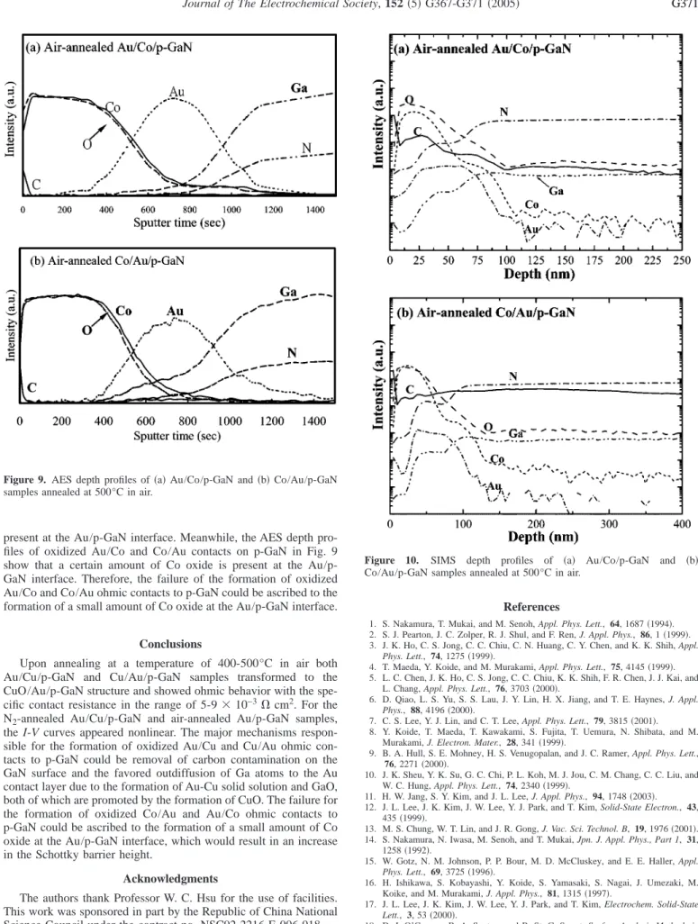
Au/Co and Co/Au contacts.—As seen in Fig. 8 the I-V curves of Au/Co and Co/Au contacts to p-GaN after annealing at 500°C in air, appear nonlinear. The AES depth profiles in Fig. 9 show that for the air-annealed Au/Co/p-GaN sample, most Co diffused out to form Co oxide on the Au surface, leaving behind a small amount of oxidized Co at the Au/p-GaN interface. For the Co/Au/p-GaN sample, most Co reacted with oxygen to form a Co oxide on the Au surface, while a small amount of Co oxide was also observed at the interface of Au/p-GaN. The presence of Co oxide at the Au/p- GaN interface can increase the Schottky barrier height.
Figure 5. XRD patterns of various samples annealed at 400°C in air show that the Au共111兲 peaks shift to the higher diffraction angles.
Figure 6. XPS peaks of Ga 2p3/2 at the interface of Au/p-GaN for 共a兲 Au/Cu/p-GaN and 共b兲 Cu/Au/p-GaN samples after annealing at 400°C in air.
The SIMS depth profiles of the air-annealed Au/Co/p-GaN and Co/Au/p-GaN samples in Fig. 10 show that after air annealing most carbon originally present on the p-GaN surface diffused into the Au layer. The reduction of carbon contamination on the p-GaN surface can improve the contacts between Au and p-GaN. In addition, the indiffusion of oxygen atoms occurred concurrently with the outdif- fusion of Ga and N atoms to the Au layer. The outdiffusion of Ga atoms would produce Ga vacancies at the GaN surface below the Au contact and thus improve the ohmic contact performance.
One of the major advantages of the SIMS technique is its excel- lent sensitivity 共⬍1 ppm兲, while its primary disadvantage is the variation of detection sensitivities over orders of magnitude for dif- ferent elements in one substrate and for the same element in differ- ent substrates.18This may be overcome to a certain extent by the use of reactive primary ions共O2
+ or Cs+兲 which enhance the yields of positive and negative ions, respectively. In the present study the sputtered ion, Cs+, was used to enhance the intensities of oxygen and carbon. However, deficiencies still exist in the capability of SIMS for quantitative elemental analysis compared to other surface analytical techniques such as AES and XPS.19AES can provide semiquantitative information directly from peak heights.18As seen in Fig. 4 the AES depth profiles of oxidized Au/Cu and Cu/Au ohmic contacts on p-GaN clearly show that almost no Cu oxide is
Figure 7. SIMS depth profiles of 共a兲 air-annealed Au/p-GaN, 共b兲 N2-annealed Au/Cu/p-GaN, 共c兲 air-annealed Au/Cu/p-GaN, and 共d兲 air-annealed Cu/Au/p-GaN samples.
Figure 8. I-V curves of Au/Co and Co/Au contact layers to p-GaN after annealing at 500°C in air, respectively.
G370 Journal of The Electrochemical Society, 152共5兲 G367-G371 共2005兲 G370
present at the Au/p-GaN interface. Meanwhile, the AES depth pro- files of oxidized Au/Co and Co/Au contacts on p-GaN in Fig. 9 show that a certain amount of Co oxide is present at the Au/p- GaN interface. Therefore, the failure of the formation of oxidized Au/Co and Co/Au ohmic contacts to p-GaN could be ascribed to the formation of a small amount of Co oxide at the Au/p-GaN interface.
Conclusions
Upon annealing at a temperature of 400-500°C in air both Au/Cu/p-GaN and Cu/Au/p-GaN samples transformed to the CuO/Au/p-GaN structure and showed ohmic behavior with the spe- cific contact resistance in the range of 5-9⫻ 10−3⍀ cm2. For the N2-annealed Au/Cu/p-GaN and air-annealed Au/p-GaN samples, the I-V curves appeared nonlinear. The major mechanisms respon- sible for the formation of oxidized Au/Cu and Cu/Au ohmic con- tacts to p-GaN could be removal of carbon contamination on the GaN surface and the favored outdiffusion of Ga atoms to the Au contact layer due to the formation of Au-Cu solid solution and GaO, both of which are promoted by the formation of CuO. The failure for the formation of oxidized Co/Au and Au/Co ohmic contacts to p-GaN could be ascribed to the formation of a small amount of Co oxide at the Au/p-GaN interface, which would result in an increase in the Schottky barrier height.
Acknowledgments
The authors thank Professor W. C. Hsu for the use of facilities.
This work was sponsored in part by the Republic of China National Science Council under the contract no. NSC92-2216-E-006-018.
National Cheng Kung University assisted in meeting the publication costs of this article.
References
1. S. Nakamura, T. Mukai, and M. Senoh, Appl. Phys. Lett., 64, 1687共1994兲.
2. S. J. Pearton, J. C. Zolper, R. J. Shul, and F. Ren, J. Appl. Phys., 86, 1共1999兲.
3. J. K. Ho, C. S. Jong, C. C. Chiu, C. N. Huang, C. Y. Chen, and K. K. Shih, Appl.
Phys. Lett., 74, 1275共1999兲.
4. T. Maeda, Y. Koide, and M. Murakami, Appl. Phys. Lett., 75, 4145共1999兲.
5. L. C. Chen, J. K. Ho, C. S. Jong, C. C. Chiu, K. K. Shih, F. R. Chen, J. J. Kai, and L. Chang, Appl. Phys. Lett., 76, 3703共2000兲.
6. D. Qiao, L. S. Yu, S. S. Lau, J. Y. Lin, H. X. Jiang, and T. E. Haynes, J. Appl.
Phys., 88, 4196共2000兲.
7. C. S. Lee, Y. J. Lin, and C. T. Lee, Appl. Phys. Lett., 79, 3815共2001兲.
8. Y. Koide, T. Maeda, T. Kawakami, S. Fujita, T. Uemura, N. Shibata, and M.
Murakami, J. Electron. Mater., 28, 341共1999兲.
9. B. A. Hull, S. E. Mohney, H. S. Venugopalan, and J. C. Ramer, Appl. Phys. Lett., 76, 2271共2000兲.
10. J. K. Sheu, Y. K. Su, G. C. Chi, P. L. Koh, M. J. Jou, C. M. Chang, C. C. Liu, and W. C. Hung, Appl. Phys. Lett., 74, 2340共1999兲.
11. H. W. Jang, S. Y. Kim, and J. L. Lee, J. Appl. Phys., 94, 1748共2003兲.
12. J. L. Lee, J. K. Kim, J. W. Lee, Y. J. Park, and T. Kim, Solid-State Electron., 43, 435共1999兲.
13. M. S. Chung, W. T. Lin, and J. R. Gong, J. Vac. Sci. Technol. B, 19, 1976共2001兲.
14. S. Nakamura, N. Iwasa, M. Senoh, and T. Mukai, Jpn. J. Appl. Phys., Part 1, 31, 1258共1992兲.
15. W. Gotz, N. M. Johnson, P. P. Bour, M. D. McCluskey, and E. E. Haller, Appl.
Phys. Lett., 69, 3725共1996兲.
16. H. Ishikawa, S. Kobayashi, Y. Koide, S. Yamasaki, S. Nagai, J. Umezaki, M.
Koike, and M. Murakami, J. Appl. Phys., 81, 1315共1997兲.
17. J. L. Lee, J. K. Kim, J. W. Lee, Y. J. Park, and T. Kim, Electrochem. Solid-State Lett., 3, 53共2000兲.
18. D. J. O’Connor, B. A. Sexton, and R. St. C. Smart, Surface Analysis Methods in Materials Science, Springer-Verlag, Berlin共1992兲.
19. A. Benninghoven, F. G. Rudenauer, and H. W. Werner, Secondary Ion Mass Spec- trometry, John Wiley & Sons, New York共1987兲.
Figure 9. AES depth profiles of共a兲 Au/Co/p-GaN and 共b兲 Co/Au/p-GaN samples annealed at 500°C in air.
Figure 10. SIMS depth profiles of 共a兲 Au/Co/p-GaN and 共b兲 Co/Au/p-GaN samples annealed at 500°C in air.