Dependence of crystal structure and work function of WN
xfilms
on the nitrogen content
Pei-Chuen Jiang, Yi-Sheng Lai, and J. S. Chena兲
Department of Materials Science and Engineering, National Cheng Kung University, Tainan 701, Taiwan 共Received 1 April 2006; accepted 18 July 2006; published online 19 September 2006兲
The effect of nitrogen content on crystal structure共phase and grain size兲 and work function 共⌽m兲 of
WNxfilms is investigated. The⌽mof WNxfilms is extracted from the plot of flatband voltage versus
SiO2 thickness. For W and WN0.4films, the⌽mare 4.67 and 4.39 V, and their crystal phases are
both body-centered-cubic W. For WN0.6 film, it contains W + W2N mixed phases and the ⌽m is
4.50 V. On the other hand, the⌽mof WN0.8and WN1.5films are 5.01 and 4.49 V, and their crystal phases are both face-centered-cubic W2N. The grain size of W and W2N phases decreases with the increase of the nitrogen content in WNx. It is concluded that the⌽mis affected by the crystal phase
as well as the grain size of WNxfilm. © 2006 American Institute of Physics.
关DOI:10.1063/1.2349313兴
Owing to the continuous downscaling of gate length and gate oxide thickness in complementary metal-oxide-semiconductor 共CMOS兲 devices, conventional polycrystal-line silicon gate electrodes suffer some problems, including high gate resistance, gate depletion, and boron penetration from the p+-doped polycrystalline silicon into the channel region.1In order to circumvent these problems, metals, metal nitrides, and metal silicides are employed as gate electrodes. Among them, the metal nitrides are the most promising ma-terials as gate electrode. Electrical properties of TiNx,2
WNx,2 TaNx,3 or HfN 共Ref. 4兲 have been investigated for
metal nitride gate electrode applications in MOS systems. However, in the metal-gate process, the major challenge is to find gate electrodes with suitable work function 共⌽m兲.
The appropriate threshold voltage in a transistor imposes that the⌽mrange of gate electrode is from 4.1 to 4.4 V for
n-channel MOS 共NMOS兲 and from 4.8 to 5.2 V for p-channel MOS共PMOS兲.1
The complexity of the CMOS integration will be less-ened when the NMOS and PMOS field effect transistors use the same gate electrode material. The advantage of using transition metal nitrides as gate electrode is due to not only their thermal stability but also their tunable⌽m. Therefore,
⌽mof the TiNx, TaNx,5MoNx,6and HfN共Ref. 7兲 have been
studied. However, the effect of nitrogen content on the⌽m
only has been addressed in Ref. 7. As for WNxfilms, the⌽m
was reported to be 5.0 V 共Ref. 8兲 or 4.64 V.9 The crystal phase of WNxwas not identified in Ref. 8 while it was W2N in Ref. 9. However, in both studies, the nitrogen content of the WNxfilm was not clear. In this study, WNxand SiO2are chosen as the gate electrode and gate dielectric, respectively. The W:N ratio of WNxis experimentally controlled and
cor-relation between⌽mand the crystal structure of WNxfilms
will be discussed.
The SiO2 film is grown on the Si substrate by thermal oxidation. The W or WNxgate electrode is then deposited on
the SiO2 layer by reactive magnetron sputtering using a W target. The total gas共Ar+N2兲 flow rate is kept at 100 SCCM 共SCCM denotes cubic centimeter per minute at STP兲 and the N2partial flow rate共the ratio of N2flow rate to the total flow
rate兲 is set at 0%, 5%, 10%, 25%, or 40% to fabricate W and WNx films of four different compositions. The radio
fre-quency共13.56 MHz兲 power supplied to the target is 150 W and the substrate holder is applied with a negative 100 V dc bias.
Atomic ratio of N / W in the films is determined by Rutherford backscattering spectrometry 共RBS兲 with 2 MeV He+ ion beams. Crystal structures of the WN
x films were
characterized by glancing incident angle x-ray diffraction 共GIAXRD兲 with Cu K␣radiation共=0.1542 nm兲 and an in-cident angle of 2°. Chemical bonding states of the films were investigated using x-ray photoelectron spectroscopy 共XPS兲 equipped with Al K␣ radiation共1486.6 eV兲. Film resistivity was obtained from sheet resistance measured by a four-point probe.
The W:N ratios of WNx films are analyzed by using
RBS. With 5%, 10%, 25%, and 40% of N2partial flow ratio during sputtering, the W:N ratios of WNx films are 1:0.4,
1:0.6, 1:0.8, and 1:1.5, respectively. Accordingly, WNxfilms
sputtered at 5%, 10%, 25%, and 40% N2 partial flow ratio are referred to as WN0.4, WN0.6, WN0.8, and WN1.5 films, respectively.
The ⌽mof WNxgate electrodes was extracted by
mea-suring the flatband voltage 共VFB兲 as a function of the gate oxide thickness, according to the following equation:10
VFB=⌽ms− Q Cox =共⌽m−⌽s兲 − Q ox t, 共1兲
where VFBis the flatband voltage of the MOS structure,⌽ms is the metal-semiconductor work function difference, ⌽s is
the work function of semiconductor, Coxis the capacitance of the oxide layer, Q is the oxide charge, t is the thickness of the oxide layer, and ox is the permittivity of oxide layer. Therefore, a measurement of VFB as a function of oxide thickness has a slope of −Q /oxand an intercept on the VFB axis of⌽ms. VFBof the WN1.5/ SiO2/ Si MOS capacitor ver-sus SiO2 thickness is plotted in Fig. 1 as an example. Ac-cordingly, by extracting the intercept from the VFB versus SiO2 thickness plot, the ⌽mvalues 共⌽m=⌽ms+⌽s兲 of WNx
共or W兲 films can be obtained and they are listed in Table I. Also listed in Table I is the correlation coefficient共r兲 of the fitting line 共r=1 for perfect fitting兲. From Table I, one can a兲Electronic mail: [email protected]
APPLIED PHYSICS LETTERS 89, 122107共2006兲
0003-6951/2006/89共12兲/122107/3/$23.00 89, 122107-1 © 2006 American Institute of Physics
see that the⌽mof WN0.8is the highest while⌽mof WN0.4is the lowest; therefore, nitrogen content of the WNxfilm is not
the only factor determining the⌽mof WNxfilm.
To understand the variation of ⌽m for WNx films, the
crystal structure of W and WNxfilms is investigated by using
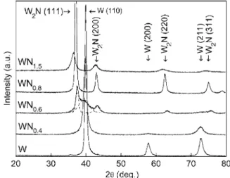
GIAXRD and the patterns are shown in Fig. 2. In addition, the 2 positions of main diffraction peaks of the films are listed in Table I. The diffraction peaks of W and WN0.4films are pertaining to共110兲, 共200兲, and 共211兲 planes of the body-centered-cubic 共bcc兲-W phase 共ICDD PDF 04-0806兲.11 The peaks of WN0.4film slightly shift to the lower 2 values as compared with those of the W film. It suggests that the lattice constant is enlarged by incorporating N atoms into the film. For the WN0.6film, the diffraction peaks are associated with 共111兲, 共200兲, 共220兲, and 共311兲 reflections from the face-centered-cubic共fcc兲-W2N phase共ICDD PDF 25-1257兲12and a broad 共110兲 reflection from the bcc-W phase, indicating that the film exhibits W + W2N mixed phases. W2N phase is the fcc structure where the W atoms occupy the positions of the fcc lattice sites and N atoms occupy 50% of the octahe-dral sites. When inserting interstitial atoms, such as nitrogen, into the bcc structure, the bcc structure distorts and transfers to fcc-like structure.13 In this case, the bcc-W 共110兲 plane transforms to the fcc-W2N 共111兲 plane. Therefore, W2N 共111兲 peak and W 共110兲 peak are close in 2position and the coexistence of these two phases is possible. The diffraction peaks of WN0.8 and WN1.5 films are associated with 共111兲, 共200兲, 共220兲, and 共311兲 reflections from the W2N phase. The 2position of the W2N共111兲 peak shifts from 37.09° 共WN0.8 film兲 to 36.53° 共WN1.5 film兲 as the nitrogen content
in-creases. The significant shift of the W2N共111兲 peak indicates that the lattice constant of the W2N crystal phase expands noticeably.
Also listed in Table I is the mean grain size of the WNx
films. The mean grain size can be estimated from the main peak breadth according to Scherrer’s formula.14Whether the film exhibits W phase 共W and WN0.4 films兲 or W2N phase 共WN0.8 and WN1.5 films兲, the resistivity 共listed in Table I兲 increases with decreasing grain size owing to the increase of electron scattering probability. Accordingly, the mean grain size analyzed from the XRD peak breadth is sensible. How-ever, the resistivity of WN0.6 is smaller than that of WN0.8 owing to the coexistence of W and W2N phases. The grain size of the WNxfilms reduces at the initial addition of
nitro-gen共WN0.4and WN0.6films兲, due to the disturbance of tung-sten lattices by adding nitrogen and the transition from bcc W to W2N. For the WN0.8film, it exhibits W2N phase with the largest grain size among all. Tungsten has a low reactiv-ity towards nitrogen and it usually requires excess nitrogen to form W–N compounds.15Our previous study on the char-acterization of reactively sputtered WNxfilms indicates that
well crystallized W2N films is overstoichiometric in nitrogen 共i.e., WN0.8兲.
16
However, the grain size of WN1.5 film re-duces again due to the much excess addition of nitrogen.
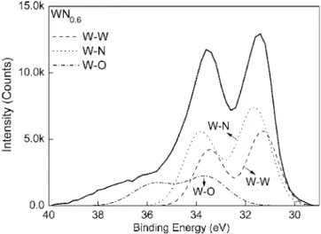
The W + W2N mixed phases in WN0.6film can also be verified by XPS and the deconvoluted W 4f XPS spectrum is depicted in Fig. 3. The surface of WN0.6film is cleaned by Ar ion beam for 10 s before taking the spectrum. It is seen that the W 4f spectrum pertains to W–W, W–N, and W–O FIG. 1. VFBof WN1.5/ SiO2/ Si structure as the function of SiO2thickness is
plotted. A measurement of VFBas a function of oxide thickness has a slope of −Q /axand an intercept on the VFBaxis of⌽ms.
TABLE I. ⌽m, correlation coefficient共r兲, 2position of the main diffraction peak, and resistivity for W and WNxfilms. The⌽mis extracted from the plot of VFBvs SiO2thickness, r is obtained by linear fitting of the VFB vs oxide thickness line, and mean grain size is estimated according to Scherrer’s formula.
Film
⌽m 共V兲
Correlation coefficient共r兲
Main peak and its 2position共deg兲 Mean grain size共nm兲 Resistivity 共⍀ cm兲 W 4.67 0.96 W共110兲: 39.92 13.9 35 WN0.4 4.39 0.99 W共110兲: 39.82 8.4 116 WN0.6 4.50 0.97 W共110兲: 39.40 2.6 174 W2N共111兲: 37.50 8.1 WN0.8 5.01 0.92 W2N共111兲: 37.09 17.1 326 WN1.5 4.49 0.95 W2N共111兲: 36.53 6.9 483
FIG. 2. GIAXRD patterns of WNxfilms with various nitrogen contents. For W and WN0.4films, the crystal phase is the bcc W. The crystal phase of the WN0.6 film is mixed W + W2N. For WN0.8 and WN1.5 films, the crystal phase is W2N.
122107-2 Jiang, Lai, and Chen Appl. Phys. Lett. 89, 122107共2006兲
bonds. The W–O bond is caused by residual oxygen in the deposition chamber. The low-energy side of the W 4f7/2– W 4f5/2doublet peaks at 31.3 and 33.5 eV are associated with the metallic W–W bond关4f7/2= 31.0 eV and 4f5/2= 33.2 eV 共Ref. 17兲兴. The W 4f7/2– W 4f5/2 doublet peaks at 31.7 and 33.8 eV shall pertain to the W2N phase 共denoted as W–N bond兲, because it locates between the W–W and W–O states. Thus, both GIAXRD and XPS analyses prove that the WN0.6 film contains W + W2N phases. By integrating the W 4f spec-trum of the W–W component and that of the W–N compo-nent individually, the W : W2N ratio in WN0.6film is calcu-lated to be 0.41:0.59. Therefore, the W2N phase is the major crystal phase in WN0.6film.
In Table I, one can see that for W and WN0.4 films, the grain size of W phase decreases from 13.9 nm 共for W兲 to 8.4 nm共for WN0.4兲 and the ⌽m decreases from 4.67 V共for
W兲 to 4.39 V 共for WN0.4兲. Similarly, for WN0.8 and WN1.5 films, the grain size of W2N phase decreases from 17.1 nm 共for WN0.8兲 to 6.9 nm 共for WN1.5兲 and the ⌽m decreases
from 5.01 V 共for WN0.8兲 to 4.49 V 共for WN1.5兲. In either case, the⌽m decreases with the decrease of the grain size.
The film with small grain indicates that it exhibits poor crys-talline quality. In addition, amorphous film has lower ⌽m
than its crystalline counterpart.18,19Therefore, the poor crys-talline quality共small grain size兲 would decrease the ⌽mof
WNxfilm. On the other hand, the W and WN0.8共W2N phase兲 films both show good crystalline quality, and the⌽m of W
共4.67 V兲 is smaller than that of WN0.8共5.01 V兲. The reason why the⌽mof W is smaller than that of WN0.8is not fully understood at present. For the WN0.6 film with W + W2N mixed phases, its⌽mis 4.50 V, which is greater than⌽mof
WN0.4 but smaller than ⌽m of WN0.8. According to W 4f XPS spectrum 共Fig. 3兲, the amount of W2N phase in the WN0.6film is larger than that of W phase. Owing to presence of the W2N phase, the ⌽m of WN0.6 共W+W2N mixed
phases兲 is larger than that of WN0.4共W phase兲.
In conclusion, we report here the impact of nitrogen con-tent on the⌽mof WNxfilms. The nitrogen content in WNx
films changes the crystal phases共W versus W2N兲 as well as the grain size. With the comparably large grain size 共⬃15–20 nm兲, ⌽mof W2N共the WN0.8film,⌽m= 5.01 V兲 is
greater than⌽mof W共4.67 V兲. Addition of nitrogen into the
large grain W and WN0.8films will decrease their grain size due to the disturbance of lattices, and the⌽mis consequently
reduced. Therefore,⌽mof WNxdoes not vary monotonically with the nitrogen content but depends on both crystal phase and grain size. With the careful control of nitrogen content, two near-Si-band-edge metal gates, i.e., WN0.4 共⌽m
= 4.39 V兲 and WN0.8 共⌽m= 5.01 V兲, could be fabricated for
NMOS and PMOS applications, respectively.
The authors gratefully appreciate the financial support from the National Science Council of Taiwan, R.O.C.共Grant Nos. NSC 93-2216-E-006-015 and NSC 94-2216-E-006-033兲. They also are greatly indebted to the Nuclear Science Technology Development Center at National Tsing Hua Uni-versity, Taiwan, for RBS facilities.
1The International Technology Roadmap for Semiconductors 共Semiconduc-tor Industry Association, San Jose, 2001兲, Front End Processes Section, p. 25.
2J. W. Lee, C. H. Han, J.-S. Park, and J. W. Park, J. Electrochem. Soc. 148, G95共2001兲.
3B. H. Lee, R. Choi, L. Kang, S. Gopalan, R. Nieh, K. Onishi, Y. Jeon, W.-J. Qi, C. Kang, and J. C. Lee, Tech. Dig. - Int. Electron Devices Meet.
2000, 39.
4H. Y. Yu, M.-F. Li, and D.-L. Kwong, IEEE Trans. Electron Devices 51, 609共2004兲.
5V. V. Afanas’eva, A. Stesmans, L. Pantisano, and T. Schram, Appl. Phys. Lett. 86, 232902共2005兲.
6B.-Y. Tsui, C.-F. Huang, and C.-H. Lu, J. Electrochem. Soc. 153, G197 共2006兲.
7H. Y. Yu, H. F. Lim, J. H. Chen, M. F. Li, C. Zhu, C. H. Tung, A. Y. Du, W. D. Wang, D. Z. Chi, and D.-L. Kwong, IEEE Electron Device Lett. 24, 230共2003兲.
8H. Matsuhashi and S. Nishikawa, Jpn. J. Appl. Phys., Part 1 33, 1293 共1994兲.
9J.-Y. Tewg, Y. Kuo, and J. Lu, J. Electrochem. Soc. 152, G643共2005兲. 10D. K. Schroder, Semiconductor Material and Device Characterization,
2nd ed.共Wiley, New York, 1998兲, Chap. 6, p. 357. 11ICDD PDF 04-0806共unpublished兲.
12ICDD PDF 25-1257共unpublished兲.
13C. Hammond, The Basics of Crystallography and Diffraction, 2nd ed. 共Oxford University Press, New York, 2001兲, Chap. 1, p. 10.
14B. D. Cullity and S. R. Stock, Elements of X-ray Diffraction, 3rd ed. 共Prentice-Hall, Englewood Cliffs, 2001兲, Chap. 5, p. 170.
15W. Ensinger and M. Kiuhci, Surf. Coat. Technol. 84, 425共1996兲. 16P.-C. Jiang, J. S. Chen, and Y. K. Lin, J. Vac. Sci. Technol. A 21, 616
共2003兲.
17C. D. Wagner, W. M. Riggs, L. E. Davis, J. F. Moulder, and G. E. Muilenberg, Handbook of X-ray Photoelectron Spectroscopy 共Perkin-Elmer, Eden Prairie, MN, 1979兲, Chap. II, p. 146.
18P. Ranade, Y.-K. Choi, D. Ha, A. Agarwal, M. Ameen, and T.-J. King, Tech. Dig. - Int. Electron Devices Meet. 2002, 363.
19W. P. Bai, S. H. Bae, H. C. Wen, S. Mathew, L. K. Bera, N. Balasubramanian, N. Yamada, M. F. Li, and D.-L. Kwong, IEEE Electron Device Lett. 26, 231共2005兲.
FIG. 3. Deconvoluted W 4f XPS spectra of WN0.6 film. For the W–W bonding state, the W 4f7/2and 4f5/2peaks are located at 31.3 and 33.5 eV. On the other hand, the W 4f7/2and 4f5/2peaks centered at 31.7 and 33.8 eV correspond to the W–N bonding state.
122107-3 Jiang, Lai, and Chen Appl. Phys. Lett. 89, 122107共2006兲