Effect of hot-carrier-induced interface states distribution on linear drain current degradation in 0.35 m n-type lateral diffused
metal-oxide-semiconductor transistors
J. R. Lee,1Jone F. Chen,1,a兲Kuo-Ming Wu,2C. M. Liu,2and S. L. Hsu2
1Institute of Microelectronics, Department of Electrical Engineering and Advanced Optoelectronic Technology Center, National Cheng Kung University, No. 1 University Road, Tainan 70101, Taiwan
2Taiwan Semiconductor Manufacturing Company, Ltd., No. 121, Park Ave. 3, Science-Based Industrial Park, Hsin-Chu 30077, Taiwan
共Received 13 December 2007; accepted 11 February 2008; published online 11 March 2008兲 The mechanisms of hot-carrier-induced linear drain current共Idlin兲 degradation in a 0.35m n-type lateral diffused metal-oxide-semiconductor transistor, operating at a nominal voltage of 12 V, is investigated. Results and analysis show that the location of hot-carrier-induced interface states varies with stress gate voltage. Stress-induced interface states located in accumulation region under polygate have little effect on Idlin degradation. As a result, interface states located in drain-side spacer region dominate Idlin degradation when interface states located in channel region are negligible. © 2008 American Institute of Physics. 关DOI:10.1063/1.2894517兴
In smart power applications, high-voltage lateral dif- fused metal-oxide-semiconductor 共LDMOS兲 transistors are widely used because of the compatibility to be integrated into standard low-voltage complementary MOS 共CMOS兲 process. Due to relatively high nominal operational voltage 共12⬃100 V兲, LDMOS transistors are prone to hot-carrier- induced degradation. Although hot-carrier-induced degrada- tion of LDMOS devices has been studied,1–8 investigation focused on the mechanism of linear drain current共Idlin兲 deg- radation 共increase of on resistance, Ron-sp兲 is necessary be- cause transistors with a lower Ron-sp produce smaller power consumption. In this paper, hot-carrier-induced Idlindegrada- tion in a n-type LDMOS device is investigated. Hot-carrier stressing under a fixed drain voltage 共Vds兲 but various gate voltages 共Vgs兲 is performed. Charge pumping measurement and technology computer-aided-design共TCAD兲 simulations 共TSUPREM4andMEDICI兲 are used to investigate the degrada- tion mechanism. Results reveal that the location of hot- carrier-induced interface states has significant impact on Idlin degradation.
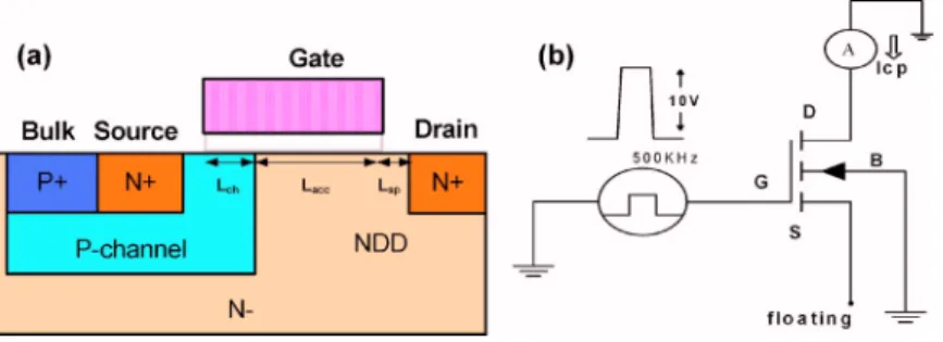
The n-type LDMOS transistor used in this paper is fab- ricated by using a standard 0.35m CMOS compatible pro- cess. Figure 1共a兲 shows schematic cross section of the de- vice. As shown in Fig.1共a兲, there are three regions between source and drain terminals, i.e., p-type channel region共Lch兲, n-type accumulation region under polygate共Lacc兲, and drain- side spacer region共Lsp兲. The gate oxide thickness of the de- vice is 30 nm and the polygate length is 0.8m. Operational voltage for both Vds and Vgs is 12 V. To accelerate hot- carrier-induced damage, stressing under Vds= 13.2 V and various Vgs ranging from 3 to 11 V for 3000 s is performed at room temperature. Idlinis measured under Vds= 0.1 V and Vgs= 12 V. Threshold voltage 共Vth兲 is extracted under Vds
= 0.1 V using maximum transconductance method. During stressing, Idlin, Vth, and charge pumping current9 共ICP兲 are monitored periodically. ICP is measured to extract stress- induced interface state density共⌬Nit兲. Figure1共b兲shows the
experimental setup of charge pumping measurement per- formed in this paper. The pulse in charge pumping measure- ment is applied to the gate while drain and bulk terminals are grounded. The source terminal is floating. The amplitude of the pulse is fixed at 10 V and base voltage 共Vbase兲 sweeps from −8 to 2 V under a frequency of 500 kHz. Rise and fall times of the pulse trains are 0.1s. All experiments are per- formed by using Agilent 4156C and an extended pulse generator.
Figure 2共a兲 shows Idlin degradation and Vth shift as a function of stress time for devices stressed under Vds
= 13.2 V and Vgsranging from 3 to 11 V. Results show that a higher Vgs produces more Idlin degradation. For devices stressed under Vgs= 3 – 9 V, Vthshift is little共⬍5 mV兲, indi- cating that hot-carrier-induced damage located in Lchregion is little. Most of the damage is located in Lacc and Lsp re- gions. However, Vthshift is more than 10 mV when the de- vice is stressed under Vgs= 11 V, revealing that damage lo- cation moves into Lch region. It has been reported that LDMOS devices exhibiting significant Kirk effect 共under high Vds and high Vgs兲 lead to serious Idlin degradation.10 Bulk current 共Ib兲 vs Vgs characteristics under various Vds shown in Fig.2共b兲indicate that Kirk effect is not significant in our LDMOS device because Ib does not increase at high Vgs 共Vgs= 12 V兲. Thus, the impact of Kirk effect on device degradation is not taken into consideration in our analysis.
To investigate the degradation mechanism, Fig. 3 ana- lyzes stress-induced increase in ICP 共⌬ICP兲 for the devices shown in Fig. 2共a兲 stressed for 3000 s. Since hot-carrier- induced⌬Nitcontributes to⌬ICPwhen the gate pulse covers Vth and flat band voltage 共Vfb兲, location dependent Vth and Vfbare investigated and the results are shown in Fig. 4. Vth and Vfbare obtained from well-calibrated TCAD simulations when the carrier concentration at Si/SiO2 interface reaches 1014cm−3for electrons and holes, respectively. Note that Vth and Vfbdrop rapidly in Lsp region because of the weak gate control. Based on Vthand Vfbdistribution obtained in Fig.4,
⌬ICP measured at Vbase= −8 V is proportional to the total
⌬Nit, i.e.,⌬Nitin Lch, Lacc, and Lspregions because the gate pulse covers Vthand Vfbin all regions. Similarly,⌬ICPmea-
a兲Electronic mail: [email protected]
APPLIED PHYSICS LETTERS 92, 103510共2008兲
0003-6951/2008/92共10兲/103510/3/$23.00 92, 103510-1 © 2008 American Institute of Physics
Downloaded 07 Oct 2009 to 140.116.208.56. Redistribution subject to AIP license or copyright; see http://apl.aip.org/apl/copyright.jsp
sured at Vbase= −2 V is proportional to ⌬Nit located in Lch and Laccregions, while⌬ICPmeasured at Vbase= 0.5 V is pro- portional to⌬Nitlocated in Lchregion only. According to the above analysis, little ⌬ICP is observed at Vbase= 0.5 V for devices stressed under Vgs= 3 – 9 V, indicating that hot- carrier-induced⌬Nitis mainly distributed in Laccand Lspre- gions. As the stress Vgsis increased to 11 V, significant⌬ICP
is observed at Vbase= 0.5 V, suggesting that significant⌬Nitis created in Lchregion. Such a result is consistent with Vthshift data in Fig.2共a兲, where Vth shift is greater under Vgs= 11 V stressing. It has been reported that Idlin degradation of con- ventional n-channel metal-oxide-semiconductor device is de- termined by total hot-carrier-induced interface states.11Such an argument, however, fails to explain Idlindegradation data when Figs.2共a兲and3are compared. Specifically, the device stressed at Vgs= 3 V has the least Idlindegradation; however,
⌬ICPmeasured at Vbase= −8 V is not the least. This indicates that not the total amount of⌬Nitbut some critical portion of
⌬Nitdominates Idlindegradation in our LDMOS devices.
To find the critical portion of ⌬Nit that dominates Idlin degradation, TCAD simulations are performed. The same amount of interface states distributed in a range of 0.05m but centered in different locations is assigned from channel to spacer edge in simulations. Idlindegradation resulted from interface states at different locations is shown in Fig.4. Re- sults reveal that interface states in Lsp region produce the most Idlindegradation. Interface states in Lchregion also de- grade Idlin but not as much as that of damage in Lsp region.
Interface states in Laccregion produce the least Idlindegrada- tion. Such a result can be explained as follows. Under Idlin measurement condition共Vds= 0.1 V, Vgs= 12 V兲, electrons in Laccregion are strongly accumulated such that electron con- centration at Si/SiO2 interface is very high. The high elec- tron density screens Coulomb scattering resulted from⌬Nit
in Laccregion. As a result, the effect of⌬Nitin Laccregion on Idlindegradation becomes less effective.12However, electron density at Si/SiO2 interface in Lsp region is relatively less because of the weak gate control. Thus, the effect of⌬Nitin Lsp region on Idlin degradation becomes severe. Results in Fig. 4 indicate that hot-carrier-induced ⌬Nit in Lsp region dominates device Idlindegradation.
To confirm the above argument, hot-carrier-induced⌬Nit
located in Lspregion is extracted from⌬ICPdata as follows:13
⌬ICP共Vbase= − 2 −⌬V兲 − ⌬ICP共Vbase= − 2兲
= qfW冕0 x0
⌬Nit共x兲dx, 共1兲
where x0is a certain location in Lspregion with x = 0 defined as the drain-side polygate edge, f is the frequency of gate pulse, and W is device width. Equation 共1兲 represents the increase of⌬ICPcaused by⌬Nitdistributed from x = 0 to x0in Lsp region. From Eq.共1兲,⌬Nitcan be extracted as follows:
⌬Nit共x兲
= − 1 qfW
⌬ICP共Vbase= − 2兲 − ⌬ICP共Vbase= − 2 −⌬V兲 dx
= − 1 qfW
d⌬Icp
dx = − 1 qfW
d⌬Icp
dVbase dVbase
dx . 共2兲
In charge pumping measurement,⌬Nitin Lspregion contrib- utes to ⌬ICP increment when Vbasesweeps below Vfb in Lsp region. Thus, the differential of Vbaseis equal to the differen- tial of Vfb, i.e., dVbase/dx=dVfb/dx. From TCAD simulation result in Fig. 4, dVfb/dx in Lsp region is roughly a constant and the value is 80.5 V/m. From ICPdata, d⌬ICP/dVbaseat Vbasebelow −2 V is also roughly a constant under different
FIG. 1. 共Color online兲 共a兲 Schematic cross section of the n-type LDMOS device used in this paper.共b兲 The experimental setup of charge pumping measurement.
FIG. 2.共Color online兲 共a兲 Idlindegradation and Vthshift as a function of stress time for devices stressed under Vds= 13.2 V and Vgsranging from 3 to 11 V.
Higher Vgsproduces more Idlindegradation, while Vthshift is little for devices stressed under Vgs= 3 – 9 V.共b兲 Ibvs Vgscharacteristics under various Vdsreveal that Kirk effect is not significant under high Vgs.
103510-2 Lee et al. Appl. Phys. Lett. 92, 103510共2008兲
Downloaded 07 Oct 2009 to 140.116.208.56. Redistribution subject to AIP license or copyright; see http://apl.aip.org/apl/copyright.jsp
stressing Vgs. Thus, the average interface states density in spacer region 共⌬Nit-sp兲 can be calculated from Eq. 共2兲 as follows:
⌬Nit-sp= 1 Lspacer冕0
Lspacer
⌬Nit共x兲dx
= − 80.5 qfWLspacer冕0
Lspacer d⌬Icp
dVbasedx
=− 80.5
qfW 冏dVd⌬Ibasecp冏Vbase=−8 Vbase=−2
, 共3兲
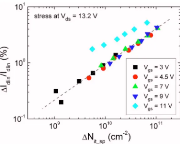
where Lspaceris the length of Lspregion. Figure5 shows the relationship between device Idlindegradation and⌬Nit-sp. For devices stressed under Vgs= 3 – 9 V, a unified relationship be- tween Idlindegradation and⌬Nit-spis obtained. For the device stressed at Vgs= 11 V, larger Idlindegradation is observed be- cause⌬Nitin Lchregion also contributes to Idlindegradation.
Results in Fig. 5 confirm that when ⌬Nit in Lch region is negligible,⌬Nitin Laccregion is not an important factor and only⌬Nitin Lspregion dominates the Idlin degradation.
In summary, mechanisms of hot-carrier-induced Idlin degradation in a n-type LDMOS transistor has been pre- sented. Charge pumping measurement and TCAD simula- tions indicate that the device degradation is mainly caused by hot-carrier-induced ⌬Nit. For devices stressed under Vgs
= 3 – 9 V, stress-induced⌬Nitare distributed in Lacc, and Lsp regions. For the device stressed under Vgs= 11 V, ⌬Nit are distributed in Lch, Lacc, and Lsp regions. Experimental data and TCAD simulations also reveal that⌬Nitlocated in Lacc region has little effect on Idlindegradation, while⌬Nitlocated in Lspregion has great impact on Idlindegradation. According to the results presented in this paper, not only the magnitude of total hot-carrier-induced⌬Nitbut also the location of⌬Nit
should be considered in evaluating the reliability of LDMOS transistors.
1R. Versari, A. Pieracci, S. Manzini, C. Contiero, and B. Ricco, Tech. Dig. - Int. Electron Devices Meet. 1997, 371.
2V. O’Donovan, S. Whiston, A. Deignan, and C. N. Chleirigh, in Proceed- ings of IEEE International Reliability Physics Symposium共IEEE, New York, 2000兲, p. 174.
3D. Brisbin, A. Strachan, and P. Chaparala, in Proceedings of IEEE International Reliability Physics Symposium 共IEEE, New York, 2002兲, p. 105.
4P. Moens, G. V. den Bosch, and G. Groeseneken,IEEE Trans. Electron Devices 51, 623共2004兲.
5P. Moens, G. V. den Bosch, C. De Keukeleire, R. Degraeve, M. Tack, and G. Groeseneken,IEEE Trans. Electron Devices 51, 1704共2004兲.
6L. Hower and S. Pendharkar, in Proceedings of IEEE International Reli- ability Physics Symposium共IEEE, New York, 2005兲, p. 545.
7J. F. Chen, K. M. Wu, K. W. Lin, Y. K. Su, and S. L. Hsu, in Proceedings of IEEE International Reliability Physics Symposium共IEEE, New York, 2005兲, p. 560.
8C. C. Cheng, K. C. Du, T. Wang, T. H. Hsieh, J. T. Tzeng, Y. C. Jong, R.
S. Liou, S. C. Pan, and S. L. Hsu, in Proceedings of IEEE International Reliability Physics Symposium共IEEE, New York, 2006兲, p. 334.
9P. Heremans, J. Witters, G. Groeseneken, and H. E. Maes,IEEE Trans.
Electron Devices 36, 1318共1989兲.
10A. W. Ludikhuize, in Proceedings of IEEE International Symposium Power Semiconductor Devices and IC’s共IEEE, New York, 1994兲, p. 249.
11J. E. Chung, P. K. Ko, and C. Hu,IEEE Trans. Electron Devices 38, 1362 共1991兲.
12S. C. Sun and J. D. Plummer, IEEE Trans. Electron Devices 27, 1497 共1980兲.
13C. Chen and T. P. Ma,IEEE Trans. Electron Devices 45, 512共1998兲.
FIG. 3. 共Color online兲 Stress-induced ⌬ICPas a function of Vbasefor the devices shown in Fig.2共a兲stressed for 3000 s.
FIG. 4. 共Color online兲 Location dependent Vthand Vfbas well as Idlindeg- radation resulted from⌬Nitat different locations are simulated. The drain- side polygate edge is defined as 0 in x coordinate.⌬Nitin Lspregion pro- duces the most Idlindegradation, while⌬Nitin Laccregion produces the least Idlindegradation.
FIG. 5. 共Color online兲 Relationship between Idlindegradation and average
⌬Nitin Lspregion is shown. A unified relationship is observed for devices stressed under Vgs= 3 – 9 V. For the device stressed at Vgs= 11 V, larger Idlin degradation is observed because⌬Nitin Lchregion also contributes to Idlin degradation.
103510-3 Lee et al. Appl. Phys. Lett. 92, 103510共2008兲
Downloaded 07 Oct 2009 to 140.116.208.56. Redistribution subject to AIP license or copyright; see http://apl.aip.org/apl/copyright.jsp