• 沒有找到結果。

Integrated Single-Inductor Buck-Boost or Boost-Boost DC-DC Converter with Power-Distributive Control

N/A
N/A
Protected

Academic year: 2021

Share "Integrated Single-Inductor Buck-Boost or Boost-Boost DC-DC Converter with Power-Distributive Control"

Copied!
4
0
0

加載中.... (立即查看全文)

全文

(1)

Integrated Single-Inductor Buck-Boost or Boost- Boost DC-DC Converter with Power-Distributive

Control

Hung-Wei Chang* ,Wei-Hsun Chang **

Dept. of Electrical Engineering National Cheng Kung University

Tainan, Taiwan

E-mail: v2696203@ee.ncku.edu.tw*

n28981280@mail.ncku.edu.tw**

Chien-Hung Tsai Dept. of Electrical Engineering National Cheng Kung University

Tainan, Taiwan E-mail: chtsai@ee.ncku.edu.tw

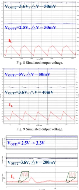
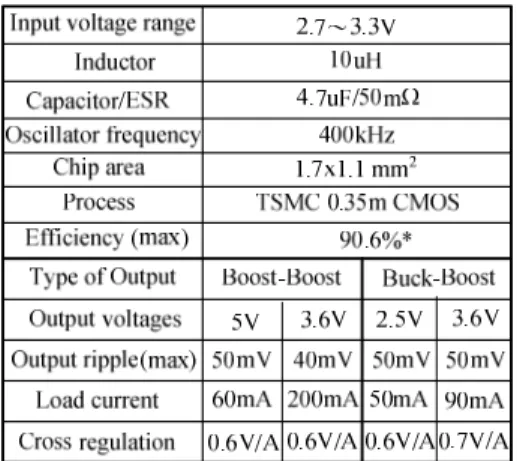
Abstract—This paper presents a fully integrated single-inductor dual-output (SIDO) buck-boost or boost-boost DC-DC converter with power-distributive control. This converter works under voltage mode control to have better noise immunity, uses fewer power switches/external compensation components to reduce cost, and is thus suitable for system on chip (SoC) applications. The proposed SIDO converter was fabricated in TSMC 0.35 μ m 2P4M CMOS technology with input supply voltage 2.7-3.3 V. The first output V O1 can operates either at buck mode or boost mode (output voltage in between 2.5V to 5V), while the second output V O2 can only operates at boost mode (output voltage 3.6V).

Keywords-component; buck/boost-boost converter; single inductor; power distributive convtrol

I. I NTRODUCTION

Today’s modern battery-operated portable products demands for advanced power management integration in SoC chips [1]. To minimize power consumption, multiple supply voltages and dynamic voltage scaling schemes are widely adopted [2]. Recently, several single-inductor multiple-output (SIMO) DC-DC converters [3-10] have been proposed as the most promising solution to minimize component (inductor and power switch) counts/footprints and production cost. However, there exists many design challenges for the SIMO converters, such as cross-regulation, efficiency, system stability, and flexibility, for achieving better step-down and step-up conversion.

The operational principles of SIMO DC-DC converters are based on time-multiplexing approaches [11], which deliver energy stored in the inductor to each output in every switching cycle by means of different feedback control mechanisms.

They can be classified as voltage control [3-5], peak current control [6-7] [10], and charge control [8-9]. In terms of inductor current waves, converters are divided into discontinuous conduction mode (DCM) [3] [7], pseudo- continuous conduction mode (PCCM) [4] [8-9], continuous conduction mode (CCM) [5], and DCM/CCM [6]. They also can be sorted into boost/boost converters [3-4] [6-7], buck/buck converters [5], and hybrid buck/boost converters [8-10] by using output voltage types. For the embedded SIMO

DC-DC converter in SoC application, although voltage control is slower than current mode control, it has no external current sensors and good noise immunity. Hence, voltage control is more suitable than current control in embedded SoC environments. Converters operated in DCM or PCCM of the conventional time-multiplexing approaches [3-4] will avoid cross-regulation, but DCM suffers large current ripples and has current driving problems. Although PCCM overcomes limitations of DCM, it dissipates unnecessary power due to non-zero current in resistance of inductor and the freewheel- switch. Converters operating in CCM suffer serious cross- regulation problems and are difficult to consider stability analysis [4]. In general, SIMO converters have to combine several compensators which have the same number of output voltage. Recently, there is a reference [6] proposes ordered power-distributive control (OPDC), which can operate in DCM/CCM, and using only one compensator. Besides, compared with familiar SIMO converters [3-4], this time- multiplexing power-distributive approach of [5-9] has less switching number in one cycle, therefore it increase efficiency.

(a) (b) (c) Fig. 1. Architecture of the buck-boost dc-dc converter.

In many applications, there are need for a single-inductor dual-output DC-DC converter with one output voltage set to be lower (buck) and another higher (boost) than the supply voltage. In traditional SIDO buck/boost converters shown in Fig.1 (a), there are five power switches [10]. Fig.1 (b) is another implementation of four power switches [8-9]. This paper adopts the Fig.1 (c) (reduce freewheel-switch S 4 of Fig.1 (b)) topology which has three power switches, and it uses power-distributive control from [6] and applies them to voltage control. Thus, there needs only one output compensation loop, which reduce the amount of external

PEDS2009

1184

(2)

compensated components used, such as [6]. Moreover, this paper also extends the availability of Fig.1(c) topology to implement Buck-Boost or Boost-Boost converter according to different demands.

In this paper, operation and control of the proposed SIDO converter and the effect of cross regulation are discussed in Section II. Section III presents circuit design and implementation issues. Post-layout simulation and results are shown in Section IV. The conclusions are given in Section IV.

II. O PERATION OF SIDO B UCK -B OOST C ONVERTER

Fig. 2. Architecture of the proposed buck-boost or boost-boost dc-dc converter.

A. Architecture and Control Strategy

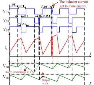
The architecture of the SIDO buck-boost or boost-boost DC-DC converter in power-distributive control with one compensator is shown Fig. 2. The output V O1 is controlled by the comparator loop, which determines the switching from V O1 to V O2 . The output V O2 is controlled by compensation loop that is responsible for compensating the total control loop.

The logic control generator is used to control the timing of the converter. The zero current detectors prevent the reversed inductor current.

DT

I L

V S2

V S1 V SX

t

I L

t V O1 <V IN

V O1 >V IN

V O2

V O1 V O2

V O2 V O1 V O2

V O1

V O1

D1T

D2T

D`T

T

V

IN

/L (V

IN

-V

O1

)/L

-(V

O2

-V

IN

)/L

V

IN

/L -(V

O1

-V

IN

)/L

-(V

O2

-V

IN

)/L

Fig. 3. Timing diagram of buck-boost or boost-boost dc-dc converter.

The operational principle is explained in the timing diagram shown in Fig. 3. The duty-cycle D is determined by PWM generator. During the DT period, the S X is turned ON, and all other switches are turned OFF. The inductor current ramps up with the slope of Vin/L until the output of the error amplifier V OP is equal to the ramp signal. S X is then turned OFF, and the inductor is connected to V O1 by turning ON S 1 . During the D 1 T, as soon as the comparator detects V O1 is larger than its target voltage, S 1 is turned OFF and the inductor is switched to V O2 . If V O1 is lower than Vin, the inductor current ramps up with the slope of (Vin-V O1 /L), otherwise ramps down with the slope of V O1 /L. That is to say V O1 can be buck or boost output During the D 2 T, the inductor current ramps down with the slope of (V O2 -Vin/L) until the next DT starts.

Fig. 4. Timing diagram of the proposed converter encounter cross regulation due to load change in V O1 .

B. Cross Regulation

The outputs of the SIMO DC-DC converter control by time- multiplexing power-distributive approaches will cross regulate among themselves, no matter in DCM or in CCM, because they are coupled together and influenced the duty cycles mutually. Our proposed converter can maintain desirable low cross-regulation which is explained in Fig. 4. Suppose that the load current suddenly increases in V O1 , which makes V O1 drop below the predetermined voltage. While detecting that, the comparator loop increases the duration, △D 1 T, to deliver more energy of inductor current to V O1 until V O1 is larger than its required voltage. Then, due to increasing external energy abruptly in V O1 , remainder energy of inductor current delivered to V O2 is decreased so that V O2 drops. In other words, the output error of the comparator-controlled V O1 is transferred and accumulated to V O2 . Receiving the voltage error of V O2 , PWM generator of the compensation loop extends the duty DT to get more energy from the inductor. At the same time, D 1 T is reduced by the comparator to maintain V O1 . Finally, V O1 and V O2 return their required voltages levels, and the proposed converter achieved low cross-regulation by

PEDS2009

1185

(3)

comparator’s fast response property.

III. C IRCUIT I MPLEMENTATION A. Logic control generator

The block diagram of the logic control generator in proposed buck-boost or boost-boost DC-DC converter is shown in Fig. 5. The logic control generator is constructed of one S-R latch and two three-input NAND logic gates. When the comparator detects the feedback voltage V FB1 of V O1 is larger than the V REF , the signal V C1 is hold on by S-R latch during the duration D’T. The output signal of S-R latch Q 1 and Q 1 _b relative to the signals V S2 and V S1 which are control output switch S 2 and S 1 , respectively. Therefore, the comparator determines the inductor connected from V O1 to V O2 . The signal V pluse reset the S-R latch every switching cycle.

The signal V PWM is generated by PWM generator. When V PWM

is active, both V S1 and V S2 are at high level so that the switch S 1 and S 2 are turned OFF. Similarly, when the inductor current is zero, the signal V ZC1 or V ZC2 is active so that the switch S 1

or S 2 is turned OFF, respectively.

Fig. 5 Block diagram of the logic controller generator.

B. Zero-current detector

The zero-current detector applies CMOS-Control Rectifier (CCR) technique [12] presented in this paper. The block diagram of CCR is shown in Fig. 6. It composes of crossed- coupled comparators and a coupling-capacitor C c . In our proposed converter, the variation of output voltage can be large in range. The comparator solves the common-mode voltage limitation in differential-input comparators with current bias. When the inductor current goes to zero, the comparator detect that the V OUT is larger than V X . Therefore, the signal V ZC is activated to prevent the reversed inductor current from V OUT to V X .

Fig. 6 Block diagram of the CCR.

IV. P OST -L AYOUT S IMULATION R ESULTS

The single-inductor dual-output buck-boost or boost-boost DC-DC converter is implemented with a TSMC 0.35μm

2P4M CMOS process. The overall layout view of SIDO converter is shown in Fig. 12. The performance is summarized in Table I. The supply voltage of converter can range from 2.7V to 3.3V. The switching frequency is 400 KHz with single inductor of 10uH. Both outputs use filtering capacitors of 4.7uF.

Fig. 8 shows the simulated output voltage of the buck-boost converter regulated at 2.5V, and 3.6V, with voltage ripple V OUT1 =50mV and V OUT2 =50mV, respectively. The output currents are I out1 =50mA, I out2 =90mA. Fig. 9 shows the simulated output voltage of the boost-boost converter regulated at 5V, and 3.6V, with voltage ripple V OUT1 =50mV and V OUT2 =40mV, respectively. The output currents are I out1 =60mA, I out2 =200mA. Fig.10 shows the results of a cross- regulation test with a supply voltage of 3V. V OUT2 is set to 3.6V, driving 90mA to its load. V OUT1 present a variation from buck output voltage of 2.5V to boost voltage of 3.3V with I OUT1 rise up from 50 to 66mA. The output voltage of V O2 drop due to the cross-regulation is less then 200mV.

Fig. 8 Simulated output voltage.

Fig. 9 Simulated output voltage.

Fig. 10 Cross-regulation simulations.

PEDS2009

1186

(4)

Fig. 11 Load-regulation simulated results.

Fig. 11 shows the simulation results of a load-regulation test. The two output voltages are set to 2.5V and 3.6V. I OUT2

has a step-up from 90mA to 180mA and vice versa while I OUT1

is fixed at 50mA.The V OUT2 voltage drop is of about 100mV.

Load regulation standards for commercial products are satisfied.

TABLE I

SUMMARY OF THE CONVERTER PERFORMANCE

Fig. 12 The layout view of the SIDO buck-boost converter.

V. C ONCLUSIONS

This paper presents a single-inductor dual-output buck-boost or boost-boost DC-DC converter in power-distributive control using only one compensator. In this work, the conventional dual-output boost converter can be extended to the buck-boost converter by substituting the voltage comparator to the error amplifier. There is no need to alter internal circuit and

compensator. Furthermore, the proposed converter requires fewer switches, uses one compensator only and reduces the circuit complexity. Compared to prior buck-boost converters, the proposed converter is more suitable for a SoC application.

A CKNOWLEDGMENT

The authors would like to thank Chip Implementation Center, Taiwan, for fabrication of the test chips. This work was supported by the National Science Council (Taiwan), under Grant NSC 098001295321.

R EFERENCES

[1] M. Hammes, C. Kranz, D. Seippel, J. Kissing, and A. Leyk, “Evolution on SoC Integration: GSM Baseband-Radio in 0.13um CMOS Extended by Fully Integrated Power Management Unit,” IEEE J. Solid-State Circuits, vol. 43, pp. 236-245, 2008.

[2] C. Yongseok, C. Naehyuck, and K. Taewhan, “DC-DC Converter- Aware Power Management for Low-Power Embedded Systems,” IEEE Trans. on Computer-Aided Design of Integrated Circuits and Systems, vol. 26, pp. 1367-1381, 2007.

[3] D. Ma, W.-H. Ki, C.-Y. Tsui, and P. K. T. Mok, “Single-inductor multiple-output switching converters with time-multiplexing control in discontinuous conduction mode,” IEEE J. Solid-State Circuits, vol. 38, pp. 89-100, Jan. 2003.

[4] D. S. Ma, W. H. Ki, and C. Y. Tsui, “A pseudo-CCM/DCM SIMO switching converter with freewheel switching,” IEEE J. Solid-State Circuits, vol. 38, pp. 1007–1014, Jun. 2003.

[5] E. Bonizzoni, F. Borghetti, P. Malcovati, F. Maloberti, and B. Niessen,

“A 200mA 93% Peak Efficiency Single-Inductor Dual-Output DC-DC Buck Converter,” IEEE Int. Solid-State Circuits Conf. Dig. Tech.

Papers, pp. 526-527, Feb. 2007.

[6] H.-P. Le, C.-S. Chae, K.-C. Lee, G.-H. Cho, S.-W. Wang, G.-H. Cho, and S.-I. Kim, “A Single-Inductor Switching DC-DC Converter with five Outputs and Ordered Power-Distributive Control,” IEEE Int. Solid- State Circuits Conf. Dig. Tech. Papers, pp. 534-535, Feb. 2007.

[7] S. -K. Hoon, N. Culp, J. Chen, and F.Maloberti, “A PWM dual-output dc/dc boost converter in a 0.13um CMOS technology for cellular phone backlight application,” Proc. European Solid-State Circuits Conference, pp.81-84, 2005.

[8] M.-H. Huang, H.-W. Huang, J.-Y. Peng, T.-L. Tsai, M.-C. Lee,C.- S.Wang, and K.-H. Chen, “Single-inductor dual-output (SIDO) DC-DC converters for minimized cross regulation and high efficiency in SoC supplying systems,” Proc. IEEE Int. Midwest Symp. Circuits and Systems, pp. 550-553, 2007.

[9] Suet-Chui Koon, Yat-Hei Lam and Wing-Hung Ki, “Integrated charge- control single-inductor dual-output step-up/step-down converter,” Proc.

IEEE Int. Symp. Circuits and Systems, pp. 3071-3074, 2005.

[10] A. Sharma and Y. S. Pavan, “A single inductor multiple output converter with adaptive delta current mode control,” Proc. IEEE Int. Symp.

Circuits and Systems, pp.4014-4018, 2006.

[11] T. Li, “Single inductor multiple output boost regulator,” U.S. Patent 6 075 295, June 2000

[12] T.Y. Man, P.K.T. Mok, and M. Chan, “A CMOS-Control Rectifier for Discontinuous-Conduction Mode Switching DC-DC Converters,” IEEE Int. Solid-State Circuits Conf. Dig. Tech. Papers, pp. 358-359, Feb 2006.

PEDS2009

1187

數據

Fig. 3. Timing diagram of buck-boost or boost-boost dc-dc converter.
Fig. 5 Block diagram of the logic controller generator.
Fig. 11 shows the simulation results of a load-regulation  test. The two output voltages are set to 2.5V and 3.6V

參考文獻

相關文件

6 《中論·觀因緣品》,《佛藏要籍選刊》第 9 冊,上海古籍出版社 1994 年版,第 1

Developmentally appropriate practice in early childhood programs serving children from birth through age 8 (3rd ed.). Washington, DC: National Association for

•  Boost invariant formula/on of the chiral kine/c theory. •   Chiral

Developmentally Appropriate Practice in Early Childhood Programs.. Washington, DC: National Association for the Education of

Developmentally Appropriate Practice in Early Childhood Programs.. Washington, DC: National Association for the Education of

Developmentally Appropriate Practice in Early Childhood Programs.. Washington, DC: National Association for the Education of

The PROM is a combinational programmable logic device (PLD) – an integrated circuit with programmable gates divided into an AND array and an OR array to provide an

➢The input code determines the generator output. ➢Understand the meaning of each dimension to control