Multi-rating Electronic Ballast for Fluorescent lamp using Phase-Locked Loop Control Scheme
Piyasawat Navaratana Na Ayudhya, Sumate Naetiladdanon and Anawach Sangswang Electrical Engineering
King Mongkut's University of Technology Thonburi Bangkok 10140, THAILAND
Email: [email protected], [email protected] and [email protected] Abstract— This paper proposes a multi-rating electronics ballast
for fluorescent lamp using phase-locked loop control scheme. By this method, the resonant frequency of the circuit is continuously tracked. Compared with the previous Phase-locked loop (PLL) control of the electronic ballasts for fluorescent lamps, the proposed method can have resonant frequency tracked for the electronic ballasts, where the equivalent resistance of the fluorescent lamps is changed. With the lamp power regulator, the proposed PLL controller commands the DC voltage to the boost converter to lock the resonant frequency. The implementation of a circuit is provided to evaluate the performance of the proposed PLL control scheme.
Keywords-multi-rating; ballast; fluorescent; phase-locked loop;
resonant
I. INTRODUCTION
The fluorescent lamps are accepted as one of the highest power efficiency lamp. These lamps are widely used in many organizations. The very weak point of using fluorescent lamps is that they need the proper ballasts to operate them at certain condition. The multi-rating fluorescent ballast was proposed to eliminate this problem. [1] and [5] proposed the automatic lamp detecting methods in order to operates the lamp at its power rating. Even those methods can operate the fluorescent lamp at the power rating; the operating frequency is not the circuit resonant. Because of the aging and manufacturing characteristic of lamps, their steady-state equivalent resistances are not always constant. Also, different types of lamps utilize the same specifications. Therefore, lamps have different levels of equivalent resistance, which leads to different voltage gains for their resonant circuits, especially in the steady state. Based on variations in lamps levels of equivalent resistance, lamp voltage cannot be accurately supported with fixed-frequency control.
The variable-frequency control [2] was proposed. Although the current control frequency method can accurately operate the lamp with desired current, changing in load resistance may cause the frequency lower or higher than the circuit (damped) resonant frequency, thus causing an increase in switching losses or losses in anti-parallel diodes. With the PLL control [3], the operating frequency can continuously track the resonant frequency (maximum voltage gain), but the voltage may be higher than the desired gain at the resonant frequency.
To improve the PLL control scheme [4] propose an external
circuit used to increase the operating frequency, and thus the voltage gain can be sufficiently reduced.
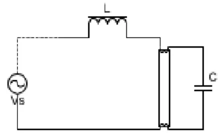
Figure 1. Simplify version of resonant inverter
However, This method cannot ensure that system will operate at resonant frequency since the frequency is limited by maximum current rating of lamp. With the fixed resonant tank and load resistance, the resonant frequency is remained as ever.
So does the voltage gain. From the simplify resonant circuit [12], the lamp power can be derived as:
Plamp = VS2Rlamp Z0 QL2 1− ω
ω0
⎛
⎝ ⎜
⎞
⎠ ⎟
⎡ 2
⎣ ⎢
⎢
⎤
⎦ ⎥
⎥
2
+ ω
ω0
⎛
⎝ ⎜
⎞
⎠ ⎟
2
(1)
Where VS = 2
π VDC,ω0= 1 LC,Z0=
L
C and QL =Rlamp Z0
From (1), with fixed lamp resistance, the lamp power is depended on ω. If ω = ω0(undamped resonant frequency where ZL = ZC) the lamp power is:
Plamp =VS2Rlamp
Z0 (2)
From (2), there is no controlled variable on the right side of equation, thus, lamp power may exceed rating. One way to reduce the output power is to reduce the input voltage that is related to DC-BUS voltage (Vs).
This paper proposes Multi-rating Fluorescent Ballast with the phase-locked loop to control DC-BUS voltage and the current feedback to control frequency. By sensing the phase
angle of voltage at the both ends of the resonant inductor, PLL commands the DC-BUS voltage. Simultaneously, by using current feedback control scheme, the lamp output power is regulated. By using this method, the damped resonant frequency, which this paper will call resonant frequency, was always tracked and run.
II. HARDWARE CONSIDERATION
This research uses typical two stages electronic ballast as shown in Fig. 2. The micro-controller controls inverter by generating square wave to the driver driving High side and low side MOSFET of the inverter.
Figure 2. Two states driving circuit consist of boost converter and resonant inverter
This micro-controller also controls DCBUS output of the PFC boost converter by driving the PFC MOSFET. Therefore, the hardware is divided into two parts consist of resonant inverter and boost converter.
A. The resonant inverter and its filter
To ensure that this ballast can be used with all T8 fluorescent lamp power ratings, the resonant parameters must be decided. There are two controlled variables that are DC input voltage and output frequency. These variables are used as constrain of resonant designing. From [5] and [6], the resonant inductor is:
Lres= VDC2η
4 frun 2π2Plamp (3) Where VDC is the DC supply voltage; η is the efficiency of inverter; frun is the running or operating frequency and Plamp is the power using by the lamp.
Using running frequency range from 25kHz to 65kHz as describe in [6], the resonant inductance is 1.9mH. Thus, this ballast can operate every T8 lamp ratings at 400 V DC supply with operating frequency between 25kHz to 65kHz. The resonant capacitance is calculated by:
C= Iph2 L
(Vph+ VDC/π )2− (VDC /π )2 (4) Where Iph is the preheat current (A); Vph is the peak preheat voltage (V) and L is the resonant inductance obtained from (3).
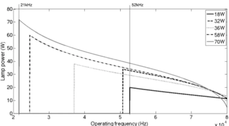
A quick substitution in (4) gives the resonant capacitance of 4.11nF. Because of availability, a typical capacitance of 4.7 nF is chosen. Once the inductance and capacitance are obtained, they are used in computer simulation to validate the operating frequency as shown in Fig. 3. The operating frequency is located between 21kHz to 52kHz where the lowest frequency is slightly lower than the originally selected frequency of 25kHz with no noticeable difference in light efficacy [7].
Figure 3. Operating frequency VS Lamp power
B. The boost converter
This boost converter is running in critical-conduction mode (CCM). This means that during each switching cycle of the PFC MOSFET, the circuit waits until the inductor current discharges to zero before turning the PFC MOSFET on again as shown in Fig. 4.
Figure 4. Line input voltage (Solid), PFC inductorcurrent (Triangle) and smoothed current (Dashed)
By this control method, the PFC inductor is:
LPFC = 8× 10⁻⁶ηVAC (rms )
(
VDC− 2VAC (rms ))
2 2POUT (5)
Where η is the efficiency of converter; VAC (rms ) is the minimum input RMS voltage; VDC is output DC voltage and
POUT is output power.
The 90V minimum input voltage (universal line), 400V maximum DC voltage and 70W maximum power giving L = 0.94mH.
III. CONTROL ALGORITHM
The block diagram of control input and output is shown in Fig. 5. The controller is divided into tree parts that are the boost converter (DC output voltage control), resonant inverter (Lamp power control) and the proposed phase-lock loop (Resonant inductor phase angle control).
Figure 5. Control signal input and output
Starting with normal ballast startup process [8], the controller controls the boost output voltage to 400V. At this state, the ballast preheats the lamp and strikes it. After the lamp is ignited, the controller controls the lamp power to its rating.
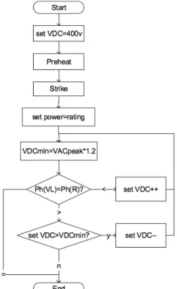
This lamp power control loop is always running until the ballast turn off. Then the phase control loop decreases or increases the VDC command until phase of the resonant inductor (ph(VL)) is equal to the resonant phase (ph(R)) or the VDC command reaches 120% of the peak AC voltage (VACpeak). This algorithm is shown in Fig. 6.
Figure 6. Flowchart of the phase locked loop algorithm
Fig. 6 is the main process includes preheat, strike power rating command and VDC command. The preheat process fixes the output frequency at 80kHz allowing the filament to be heated by small amount of current. Then the ballast decreases the frequency to increase lamp voltage until the current start to flow through to the lamp tube. This controller can detect the lamp ignition by monitoring the lamp voltage. If the voltage is suddenly dropped down when decreasing the output frequency, the lamp is ignited. After that, the lamp power rating detection is happening. The algorithm returns the lamp power command to the Lamp power control procedure as shown in Fig. 7.
Figure 7. PLL controller block diagram and input/output signal
A. Lamp power control
The operating frequency plays an important role since the lamp power is increased as the frequency is reduced. The inverter must operate under proper frequency to avoid lamp damages. The current regulation method will control the lamp power within its rating [4]. The average voltage of the Rsinv on the low side driver MOSFET in Fig. 2 represents the current through the half-bridge driver as described in [1] and [2]. The algorithm flowchart is shown in Fig. 8.
Figure 8. Flowchart of the lamp power control algorithm
This procedure is trigged by the internal 1ms timer.
Therefore, this procedure runs continual using the given power
command. The block diagram of this control part is shown in Fig. 9.
Figure 9. Block diagram of the lamp power control
B. Boost converter
This part takes an important role in this control scheme.
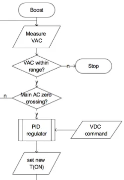
This converter is implemented using the method from [9]. By using this retriggerable one-shot module embedded in the microcontroller, this converter use less processing time. Thus, there is sufficient processing time left for PLL process. The boost converter control algorithm is shown in Fig. 10 and the block diagram is shown in Fig. 11.
As the power regulation procedure, this procedure operates continuously using the given VDC command.
Figure 10. Flowchart of the boost converter control algorithm
Figure 11. Blockdiagram of the boost converter
IV. THE SIMULATION RESULTS
In order to simulate the lamp ignition and steady state, the fix resistance 100kΩ(R1), 1kΩ(R2), 500Ω(R3) and 100Ω(R4) are setting up. The results are shown in Fig. 11.
Figure 12. Gains (dB) and Phase (degree) of Vout/Vin
The Fig. 12 shows the gain and phase of output voltage to the input with resistance from 100kΩ down to 100Ω. When the lamp resistance is higher than 100kΩ, the resonant is at the ω0 (the damped resonant frequency is equal to the undamped resonant frequency). This state occurs before lamp ignition. By decreasing the output frequency, the output voltage is increased. When the lamp voltage is high enough for emitting electrons into the gas column, the lamp is ignited. After that, the lamp presents a negative differential resistance to the resonant circuit as shown in Fig. 13.
Figure 13. The V-I characteristic of 32WT8 lamp[10]
With the serial inductor, the lamp presents as a stable resistance when the frequency is fixed. This is caused by the inductor limits the lamp current depending on the input
frequency. From Fig. 13, the 32W lamp resistance can vary from 500Ω at the 100% power rating to 8kΩ at the 20% power rating. Fig. 12 shows that the resonant frequency moves to the left when the resistance is decreasing. When running with 1kΩ and 500Ω in sequence, the resonant frequencies are 49kHz and 28kHz.
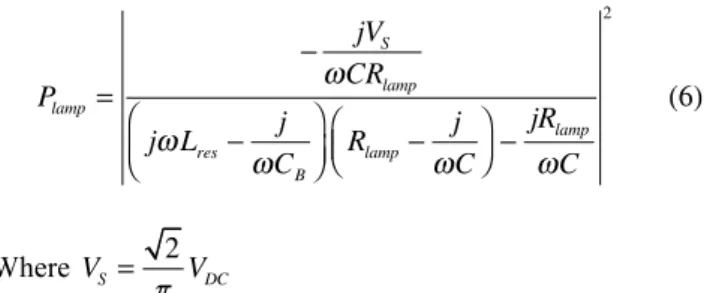
To simulate the lamp operating condition, the dynamic lamp model and the simplify version of inverter is used. Lamp power can be calculated using:
Plamp=
− jVS ωCRlamp jωLres− j
ωCB
⎛
⎝⎜
⎞
⎠⎟ Rlamp− j ωC
⎛⎝⎜ ⎞
⎠⎟ − jRlamp
ωC
2
(6)
Where VS = 2 π VDC
From [10] the negative differential resistance of fluorescent is simplified as;
Rlamp = V0RS V0− VH
(7)
where V0 is the voltage at present condition and RSand VH are defined as;
RS =VMax− Vmin
IMax− Imin (8) VH = Vmin− IminRS (9) Where VMax is lamp voltage at the highest power; Vmin is the lamp voltage at the lowest power; IMax is the lamp current at the highest power and Imin is the lamp current at the lowest power.
These parameters were acquired from [11]. To simulate the results, assume the initial Rlamp is 1kΩ. Calculate the current using this resistance. Then the new V0 is calculated using V= IR. Using this V0 to calculate the new Rlamp. Recalculate the current and Rlamp until the current is stable. Then the lamp power from this current is calculated. If the lamp power is less than the power command then reduce the frequency and recalculate the lamp power. Repeat these procedures until lamp power is equal to the power command.
The operating frequency of the 32W lamp using with the designed ballast is 50kHz at 400VDC supply. This frequency is not resonant frequency since the resonant is 28kHz. Decreasing frequency below 50kHz will damage the lamp by over wattage.
Thus, the frequency variation cannot operate the lamp at its resonant.
From (6), the variation of input voltage affects the operating frequency. Decreasing the DC voltage results the lower lamp power. With lamp power less than the power command, the lamp power controller decreases the driving frequency until both lamps power and power command are equal. At 32W lamp power, the lower DC voltage results lower operating frequency. But, too low DC voltage will lead to hard switching and the lamp will not reach the power rating.
The phase locked loop control is widely used in the application that needs to operate at the resonant frequency. The phase angle to be locked is -90°. Unfortunately, the resistance of fluorescent lamp is lower than 1kΩ at the 100% power rating. This results the higher phase angle at resonant frequency depending on the lamp resistance. Therefore, this presented phase locked loop controller has difference phase command for each lamp power rating. The phase commands are shown in table I.
V. EXPERIMENTAL RESULTS
There are 4 sets of experiments include
• Fix DC command at 400V and operate the lamp at power rating to find the lamp resistances, running frequencies and phase angles.
• Substitute the lamps with the resistors and vary the operating frequency to find the resonant frequencies and phase angles.
• Using PLL to command the DC voltage and supply the ballast with 90VAC. Measure the running frequencies and phase angles.
With 400V DC command, the lamps resistances, running frequencies and phase angles are shown in table I.
TABLE I. THE LAMP RESISTANCE , RUNNING FREQUENCY AND PHASE ANGLE WHILE RUNNING LAMP AT FULL POWER AND DC COMMAND IS 400V.
Lamp power rating
(W)
Resistance at 100% power
(Ω)
Running frequency
(kHz)
Phase angle (°)
18 267 56 -95
32 425 52 -90
36 276 39 -80
58 220 28 -65
70 236 26 -60
When substitute the lamps with the resisters, the resonant frequencies and phase angles are measured.
TABLE II. THE RESONANT FREQUENCIES AND PHASE ANGLES OF THE CIRCUIT RUNNING WITH THE RESISTANCE LOADS.
Lamp power rating
(W)
Resistance at 100% power
(Ω)
Resonant frequency (kHz)
Resonant phase angle (°)
18 267 13 -30
32 425 18 -30
36 276 13 -30
58 220 12 -35
70 236 12 -35
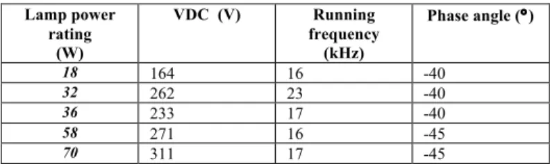
To avoid the hard switching, the phase commands are set at 10° lower than the resonant phase angle. To let VDC command as low as possible, the 90VAC is supplied. The results of the proposed PLL control scheme are shown in table III.
TABLE III. THE RUNNING DC SUPPLY VOLTAGES, RUNNING FREQUENCIES AND PHASE ANGLES OF THE PLL CONTROL SCHEME. Lamp power
rating (W)
VDC (V) Running frequency
(kHz)
Phase angle (°)
18 164 16 -40
32 262 23 -40
36 233 17 -40
58 271 16 -45
70 311 17 -45
From the experimental results, the running frequencies of the proposed control scheme are closer to the resonant frequencies than those of the previous fixed DC control scheme. There are three more things to be concerned.
• Boost converter cannot drive out the voltage equal or below the peak AC voltage. Thus, the actual operating frequency is highly depending on AC voltage.
• The phase command must be set lower than the resonant since the current regulator loop will easily go below the resonant and cause the increase in switching loss plus the lamp will not meet the operating power.
• With this control method, the inverter efficiency is increased by around 1-2%. This will occur only when the DC-BUS voltage can be decreased to the proper value of each lamp. As the results of DC voltage decreased, the conduction losses in the boost converter are also reduced.
VI. CONCLUSION
This paper proposes Multi-rating Fluorescent Ballast with the phase-locked loop control DC-BUS voltage and the current feedback control frequency. By sensing the phase angle of voltage at the both ends of the resonant inductor, PLL commands the DC-BUS voltage. Simultaneously, by using current feedback control scheme, the lamp output power is
regulated. By using this method, the resonant frequency was always tracked and run. The result of this tracking eminently depends on the AC input voltage that limits the boost converter output not to goes below the peak input voltage.
REFERENCES
[1] L. Lee, S. Hui, and H. Chung, “An automatic lamp detection technique for electronic ballasts.”, IEEE Applied Power Electronics Conference and Exposition, 2005, 1:575–581 Vol. 1, March 2005.
[2] F. Rodriguez, J. Ribas, and J. M. Alonso, “Analysis and design of the LCC-parallel series inverter with resonant current control as HPS lamp ballast”, in Proc. IEEE 32nd Annu. Power Electronics Specialists Conf.
(PESC’01), vol. 2, Jun. 17–21, 2001, pp. 980–985.
[3] C.-H. Lin, Y. Lu, K.-J. Pai, and Y.-Q. Chen, “Achieving maximum- efficiency tracking control for backlight electronic ballast with phase- locked loop techniques”, in Proc. IEEE Int. Conf. Control Applications, vol. 2, Sep. 2–4, 2004, pp. 1651–1656.
[4] R.-L. Lin and Y.-T. Chen., "Electronic ballast for fluorescent lamps with phase-locked loop control scheme", IEEE Transactions on Power Electronics, 21(1):254–262, Jan. 2006.
[5] P. Navaratana, S. Naetiladdanon, and A. Sangswang, “Automatic fluorescent lamp detection technique for electronic ballasts.”, IEEE International Conference on Robotics and Biomimetics, February 2009.
[6] P. Navaratana, S. Naetiladdanon, and A. Sangswang. “Automatic fluorescent lamp detection for electronic ballasts based on operating frequency and phase shift compensation.” IEEE International Symposium of Industrial Electronics, July 2009.
[7] John, E. Kaufman, and J. F. Christensen., IES Lighting Handbook., Illuminating Engineering Society, 1984.
[8] T. Ribarich and J. Ribarich., “A new procedure for high-frequency electronic ballast design.”, IEEE Transactions on Industry Applications, 37(1):262–267, Jan/Feb 2001.
[9] D. He, W. Dilliard, and R. Nelms., “Microcontroller implementation of current-mode control for a discontinuous mode boost converter.”, In Energy Conversion Engineering Conference, 2002. IECEC ’02. 2002 37th Intersociety, pages 255–260, July 2002.
[10] T.-F. Wu, J.-C. Hung, and T.-H. Yu., “A pspice model for fluorescent lamps operated at high frequencies”. 21st International Conference on Industrial Electronics, Control, and Instrumentation, 1995., Proceedings of the 1995 IEEE IECON, 1:359–364 vol.1, Nov 1995.
[11] I. R. Corporation. Ir ballast designer version 4.1.7. PC Software, 2006.
[12] Z. Li, P. Mok, W.-H. Ki, and J. Sin., “A simple method to design resonant circuits of electronic ballast for fluorescent lamps.”, Proceedings of IEEE International Symposium on Circuits and Systems, volume 3, pages 1744–1747 vol.3, Jun 1997.