ized aperture-coupled microstrip antennas, IEEE Trans Antennas Propa-gat AP-41 (1993), 214 –220.
4. C.Y. Huang, J.Y. Wu, and K.L. Wong, Cross-slot-coupled microstrip antenna and dielectric resonator antenna for circular polarization, IEEE Trans Antennas Propagat AP-47 (1999), 605– 609.
5. S.D. Targonski and D.M. Pozar, Design of wideband circularly polar-ized aperture-coupled microstrip antennas, IEEE Trans Antennas Propa-gat AP-41 (1993), 214 –220.
© 2005 Wiley Periodicals, Inc.
AN IMPROVED APPROACH FOR
SMALL-SIGNAL EQUIVALENT-CIRCUIT
PARAMETER DETERMINATION OF
InGaP/GaAs HBT
Han-Yu Chen,1Kun-Ming Chen,2Guo-Wei Huang,2 Chun-Yen Chang,1and Tiao-Yuan Huang1
1Institute of Electronics
National Chiao-Tung University Hsinchu, 300 Taiwan
2National Nano Device Laboratories
1001-1 Ta Hsueh RD. Hsinchu 300, Taiwan
Received 2 August 2004
ABSTRACT: In this paper, an improved method for extracting the
small-signal equivalent-circuit elements of an HBT is proposed. A more general HBT equivalent circuit and a more general explicit equation on the total extrinsic elements are introduced. Linear least-square algo-rithms are cleverly adopted to reduce the number of error function. As a result, the modified approach can yield a better fit between the measured and simulated S-parameters over the conventional method. © 2005 Wiley
Periodicals, Inc. Microwave Opt Technol Lett 44: 456 – 460, 2005; Published online in Wiley InterScience (www.interscience.wiley.com). DOI 10.1002/mop.20666
Key words: HBT; device modeling; small-signal modeling; parameter
extraction; microwave transistor
1. INTRODUCTION
In recent years, much effort has been devoted to analytical ap-proaches of HBT equivalent-circuit parameter extraction [1– 6]. Many closed-form representations of intrinsic circuit elements have been derived for direct extraction of equivalent-circuit ele-ments [3– 6]. However, direct-extraction techniques are sensitive to the accuracy of extracted extrinsic parameters. At microwave frequencies, it has been noted that a slight change in any of the extrinsic elements’ value could result in drastic changes in the intrinsic elements’ value [7, 8]. Therefore, a strong correlation exists between the extrinsic and intrinsic circuit elements. Based on this correlation, Shirakawa et al. [7] and Ooi et al. [8] proposed a technique to determine the FET equivalent-circuit elements, which does not require additional measurements other than the
S-parameters. Recently, the technique has been extended to HBT
equivalent-circuit modeling [4, 5]. To reduce the optimization variables, the assumption that the imaginary part of Z12of an HBT tends toward zero is adopted to establish the relation between extrinsic inductance and other circuit elements. Although the re-duction of optimization variables greatly saves computer time, it may cause the modeling routine to be trapped in a local minimum, due possibly to a nongeneral assumption, since the imaginary part of Z12of an HBT shows a frequency response in most situations.
In this paper, a more general HBT equivalent circuit, which separates the base/emitter delay from base/emitter RC circuit and takes into consideration the finite resistance between the base and collector, is used to improve the methods in [4, 5]. A more general analytic equation, which establishes the relationship between ex-trinsic inductance and other circuit elements, is introduced to avoid the abovementioned problem. In addition, linear least-square al-gorithms are cleverly adopted to reduce the number of error function, and only six intrinsic circuit elements are involved during optimization.
2. EQUIVALENT CIRCUIT OF THE HBT TRANSISTOR As shown in Figure 1(a), a general equivalent circuit for InGaP/ GaAs HBT is used in this study. As indicated in this figure, the equivalent circuit is divided into three parts. The Level-2 part excludes the elements RE, LE, RB, LB, RC, and LCfrom Level 1,
while the part of Level 3 excludes the element Cbcxfrom Level 2.
In Figure 1(b), the equivalent circuit of Level 2 in the common-collector configuration is shown. The respective ABCD parame-ters, ALevel2, are described as follows:
ALevel2⫽
冋
A11,Level2 A12,Level2
A21,Level2 A22,Level2
册
, (1)where
A11,Level2⫽ 1 ⫹ RbiYbc, (2a)
Figure 1 Equivalent circuit of (a) an InGaP/GaAs HBT and (b) Level 2 in the common collector configuration
A12,Level2⫽ Rbi共1 ⫺␣兲 ⫹ 1 Ybe共1 ⫹ R biYbc兲, (2b) A21,Level2⫽ Ybc⫹ Yex共1 ⫹ RbiYbc兲, (2c) A22,Level2⫽ 共1 ⫺␣兲共1 ⫹ RbiYex兲 ⫹ 1 Ybe关Y bc⫹ Yex共1 ⫹ RbiYbc兲兴, (2d) with Ybc⫽ 1 Rbci⫹ jC bct, (3a) Ybe⫽ 1 Rbe⫹ jC be, (3b) Yex⫽ jCbcx. (3c)
The transformation between the Y-parameters of the common-emitter configuration (Ye) and the Y-parameters of the
common-collector configuration (Yc) are given by
Yc⫽
冋
Y11,e ⫺共Y11,e⫹ Y12,e兲
⫺共Y11,e⫹ Y21,e兲 共Y11,e⫹ Y12,e⫹ Y21,e⫹ Y22,e兲
册
. (4)The extrinsic part of the HBT, which is located outside Level 2, is related to Level 2 through the following expressions:
ZLevel2⫽ ZLevel1⫺ Zext, (5)
Zext⫽
冋
RE⫹ RB⫹ j共LE⫹ LB兲 RE⫹ j共LE兲
RE⫹ j共LE兲 RE⫹ RC⫹ j共LE⫹ LC兲
册
, (6) where ZLevel1and Zextare the overall and extrinsic Z-parameters,
respectively.
3. ANALYTICAL DETERMINATION OF THE EQUIVALENT-CIRCUIT ELEMENTS
Similar to conventional FET modeling, once the extrinsic elements are known, the intrinsic elements can be determined analytically. The overall measured S-parameters are first converted to Z-param-eters, and by using Eqs. (5) and (6), the Z-parameters in the common-emitter configuration of Level 2 are obtained. By using Eq. (4) and standard network-parameter transformation, the ABCD parameters in common-collector configuration of Level 2, Alevel2,
are obtained. Based on the equivalent circuit shown in Figure 1(b), the equivalent-circuit elements in Level 2 are derived as follows:
Rbc⫽ 1 Re共Ybc兲 , (7a) Rbe⫽ 1 Re共Ybe兲 , (7b) Cbci⫽ Im共Ybc兲 , (7c) Cbe⫽ Im共Ybe兲 , (7d) Cbcx⫽ Im共Yex兲 , (7e) Rbi⫽
Re关共A11,level2⫺ 1兲A*11,level2兴
Re关A21,level2A*11,level2兴
, (7f)
␣ ⫽ 1 ⫺ 共 A11,Level2A22,Level2⫺ A12,Level2A21,Level2兲, (7g)
with
Yex⫽
⫺Re关共A11,level2⫺ 1兲A*21,level2兴
Re关共A11,level2⫺ 1兲A*11,level2兴
, (8a) Ybc⫽ 共 A11,level2⫺ 1兲 Rb2 , (8b) Ybe⫽ Ybc 共 A22,level2⫺ YexA12,level2⫹␣ ⫺ 1兲 . (8c)
The three parameters of␣0,, and f␣, are determined directly from the frequency dependence of Eq. (7g) with linear least-square algorithms. The parameters␣0and f␣are first extracted from兩␣兩2,
which leads to the linear least-squares problem:
min
冘
n⫽1 N冋
兩␣共n兲兩2⫹ fn 2兩␣共 n兲兩2 f␣2 ⫺␣02册
2 , (9)where w and N are the angular frequency and the number of measured frequencies, respectively. The transit time is then calculated using the mean value of
⫽ ⫺1
冋
⬔␣ ⫹ tan⫺1冉
ff␣
冊册
. (10)The advantage of using linear least-squares algorithms is that the parameters␣0,, and f␣ can be directly solved by linear matrix calculation, thus greatly reducing the number of error functions used for determining the extrinsic circuit elements.
As shown in Figure 1(a), since the imaginary part of
Z11,Level3⫺ Z12,Level3is zero [6], a general analytic equation in terms of the equivalent-circuit elements can be found, which is reproduced here as LB⫹ CbcxCbciRbiRB Cbcx⫹ Cbci ⫺ CbcxCbciRbi Cbcx⫹ Cbci Re共Z11,Level1⫺ Z12,Level1兲
⫺ Im共Z11,Level1⫺ Z12,Level1兲 ⫽ 0. (11)
From Eq. (11), the extrinsic elements, LB can be expressed in
terms of the other extrinsic elements as follows:
LB⫽ f0共wi, LC, LE, RB, RC, RE兲 ⫽ f0共i, Zext⫺ LB兲. (12)
The representation Zext ⫺ LB denotes all the extrinsic elements
except the base inductance. So, once the values of RB, RC, RE, LC,
and LEare known, LBcan be determined. By substituting Eq. (12)
into Eq. (7), the intrinsic elements can be expressed in a similar way as follows:
Cbcx⫽ f2共i, Zext⫺ LB兲, (13b)
Rbe⫽ f3共i, Zext⫺ LB兲, (13c)
Cbe⫽ f4共i, Zext⫺ LB兲, (13d)
Rbc⫽ f5共i, Zext⫺ LB兲, (13e)
Cbci⫽ f6共i, Zext⫺ LB兲. (13f)
If the extracted equivalent circuit elements are valid at every measured frequency, the elements’ values will depict negligible frequency response. By finding the specific extrinsic elements RB,
RC, RE, LC, and LE, which minimize the frequency dependence of
the intrinsic elements, the equivalent-circuit modeling is reduced to an optimization problem of finding the specific five extrinsic elements.
4. THE EXTRACTION ALGORITHM AND RESULTS
In our proposed method, the first objective function is to optimize the extrinsic elements so that the intrinsic elements exhibit less frequency dependence; this is expressed as
E1k 共RB, RC, RE, LC, LE兲 ⫽ 1 N⫺ 1 ⫻
冘
i⫽0 N⫺1冏
kfk共i, Zext⫺ LB兲 ⫺冘
j⫽0 N⫺1 kfk共j, Zext⫺ LB兲冏
2 , (14)where k varies from 1 to 6, the over bar indicates the mean values, and k is a normalizing factor to make the values of fk vary
between zero and one.
For stable calculation of the S-parameters, the second objective function, Eq. (15), is considered as a loose constraint:
E2k 共RB, RC, RE, LC, LE兲 ⫽
冘
p⫽1 2冘
q⫽1 2冘
i⫽0 N⫺1 ⫻ Wpq兩Spq c 共wi, Zext⫺ LB兲 ⫺ Spq m 共i, Zext⫺ LB兲兩2, (15)where the superscripts c and m denote the calculated and measured
S-parameters, respectively, and Wpqis the weighting factor of Spq.
The mean values of intrinsic elements are used for computing Spq C
and LB. The extended error vector is then composed of
共i, RB, RC, RE, LC, LE兲 ⫽
冤
冘
k⫽1 6 E1k 共RB, RC, RE, LC, LE兲 E2k 共RB, RC, RE, LC, LE兲冥
. (16) As indicated initially in Figure 2, the values of extrinsic pa-rameters RB, RC, RE, LC, and LEare selectively assignedaccord-ing to their appropriate range. Hence, the extrinsic parameters are close to the physically meaningful minimum of the optimization error function. Then, the extrinsic inductance LB and all the
parameters within the Level-2 part are evaluated from Eqs. (11) and (7). The process is conducted iteratively in order to make Eq. (16) minimum. If the error vector of Eq. (16) is below the designed error criteria, the extrinsic and intrinsic elements will be extracted and thus the equivalent-circuit modeling is completed.
To validate the accuracy of the proposed extraction technique, several InGaP/GaAs HBTs fabricated in house [9] were investi-gated. The flowchart shown in Figure 2 was implemented on Agilent IC-CAP EESoft.
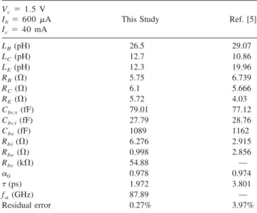
Figure 3 shows a comparison between the measured and cal-culated S-parameters, for both our proposed method and the con-ventional method [5]. As shown in Figure 3, both methods yield good agreement over the entire frequency range. For ease of comparison, no parameter reduction was used in the conventional equivalent circuit extraction method. Table 1 gives a comparison of the modeling results and the residual error, quantifying the accuracy for both the conventional method and proposed method according to 储储 ⫽4N1
冘
p⫽1 2冘
q⫽1 2冘
i⫽0 N⫺1 兩Spq c 共i兲 ⫺ Spq m 共i兲兩 兩max共Spq m共 i兲兲兩 . (17)A smaller residual error is observed in the proposed method. The reason for this may be that more complete intrinsic circuit ele-ments are used in this study (nine in the proposed method, seven
in the conventional method). Also, fewer error functions (seven in the proposed method, eight in the conventional method) and fewer optimization variables (five in the proposed method, six in the conventional method) are involved in the proposed method, and thus greatly reduce the complexity of the optimization routine and
increase the possibility of escaping from the local minimum during the optimization procedure.
5. CONCLUSION
An improved and more efficient technique for small-signal HBT equivalent circuit parameter extraction has been introduced. Com-paring with the conventional method, the closed-form representa-tion of a more general T-topology circuit with nine intrinsic circuit elements has been presented. The transistor parameters␣0,, and
f␣are cleverly derived with least-square algorithms, which reduce the number of error functions used to determine the extrinsic elements. Also, a more general explicit equation for the total extrinsic elements has been derived, resulting in a reduction of the number of optimization variables. As a result, a better fit between the measured and simulated S-parameters is achieved, as compared to the conventional method.
ACKNOWLEDGMENTS
The authors would like to thank Prof. Edward Yi Chang of NCTU for providing the HBTs used in this study and the staff members of NDL for measurement support.
REFERENCES
1. D. Costa, W.L. Liu, and J.S. Harris, Direct extraction of the AlGaAs/ GaAs heterojunction bipolar transistor small-signal equivalent circuit, IEEE Trans Electron Devices 38 (1991), 2018 –2024.
2. D.R. Pehlke and D. Pavlidis, Evaluation of the factors determining HBT high-frequency performance by direct analysis of s-parameter data, IEEE Trans Microwave Theory Tech 40 (1992), 2367–2373. 3. B.L. Ooi, T.S. Zhou, and P.S. Kooi, AlGaAs/GaAs HBT model
esti-mation through the generalized pencil-of-function method, IEEE Trans Microwave Theory Tech 49 (2001), 1289 –1294.
4. T.S. Zhou, B.L. Ooi, and P.S. Kooi, A novel approach for determining the AlGaAs/GaAs HBT small-signal equivalent circuit elements, Mi-crowave Opt Technol Lett 28 (2001), 278 –282.
5. B.L. Ooi, T.S. Zhou, and P.S. Kooi, Efficient method for heterojunction bipolar transistor model parameter extraction based on correlation be-tween extrinsic and intrinsic elements, Int J RF and Microwave CAE 12 (2002), 311–319.
6. B. Sheinman, E. Wasige, M. Rudolph, R. Doerner, V. Sidorov, S. Cohen, and D. Ritter, A peeling algorithm for extraction of the HBT Figure 3 Simulated (—) and measured (䊐) S-parameters from 1 to 25
GHz biased at Vc⫽ 1.5 V and Ic ⫽ 40 mA for the (a) new and (b)
conventional methods
TABLE 1 Modeling Results and Related Residual Data-Fitting Errors for our Proposed Method and Conventional Method
Vc⫽ 1.5 V
Ib⫽ 600A This Study Ref. [5]
Ic⫽ 40 mA LB(pH) 26.5 29.07 LC(pH) 12.7 10.86 LE(pH) 12.3 19.96 RB(⍀) 5.75 6.739 RC(⍀) 6.1 5.666 RE(⍀) 5.72 4.03 Cbcx(fF) 79.01 77.12 Cbci(fF) 27.79 28.76 Cbe(fF) 1089 1162 Rbi(⍀) 6.276 2.915 Rbe(⍀) 0.998 2.856 Rbc(k⍀) 54.88 — ␣0 0.978 0.974 (ps) 1.972 3.801 f␣(GHz) 87.89 — Residual error 0.27% 3.97%
small-signal equivalent circuit, IEEE Trans Microwave Theory Tech 50 (2002), 2804 –2810.
7. K. Shirakawa, H. Oikawa, T. Shimura, Y. Kawasaki, Y. Ohashi, T. Saito, and Y. Daido, An approach to determining an equivalent circuit for HEMT’s, IEEE Trans Microwave Theory Tech 43 (1995), 499 –503. 8. B.L. Ooi, M.S. Leong, and P.S. Kooi, A novel approach for determining the GaAs MESFET small-signal equivalent-circuit elements, IEEE Trans Microwave Theory Tech 45 (1997), 2084 –2088.
9. S.-W. Chang, E.Y. Chang, C.-S. Lee, K.-S. Chen, C.-W. Tseng, and T.-L. Hseih, Use of WNxas the diffusion barrier for interconnect copper
metallization of InGaP-GaAs HBTs, IEEE Trans Electron Devices 51 (2004), 1053–1059.
© 2005 Wiley Periodicals, Inc.
A THREE-DIMENSIONAL PLANAR
PHOTONIC CRYSTAL USING
CONDUCTING POLYMERS
L. Oyhenart, V. Vigne´ras, F. Demontoux, and J. P. Parneix Laboratoire de Physique des Interactions Ondes-Matie`re (PIOM) UMR CNRS 5501
ENSCPB, 16 Avenue Pey-Berland 33607 Pessac, France
Received 29 July 2004
ABSTRACT: In this paper, we study the possibility of replacing metal
by conducting polymer in the formation of 3D metallic photonic crys-tals. Subject to obtaining the highest conductivity, it is possible to obtain similar comportment between metallic and polyaniline structures. As-pects of technological interest, such as reduction of cost and the weight of the structure, are discussed. © 2005 Wiley Periodicals, Inc.
Microwave Opt Technol Lett 44: 460 – 463, 2005; Published online in Wiley InterScience (www.interscience.wiley.com). DOI 10.1002/mop. 20667
Key words: photonic crystal; photonic band gap; conducting polymer;
polyaniline; technology
1. INTRODUCTION
Throughout the past decade, there has been a great deal of interest in photonic crystals [1], which are periodic dielectric materials capable of inhibiting the propagation of light over the spectral region known as the photonic band gap (PBG). Thus numerous applications of photonic crystals have been proposed for improv-ing the performance of devices with operatimprov-ing frequencies rangimprov-ing from the microwave to optical, including zero-threshold lasers, novel resonators and cavities, and efficient microwave antennas [2, 3]. Although the use of photonic crystals made of dielectric ma-terials has been successful in various applications, some properties restrict usage. Metals exhibit high absorption at optical frequen-cies; they act like nearly perfect conductors at lower microwave and millimeter-wave frequencies that minimize the problems re-lated to absorption. A metallic structure can made at a substantially reduced size and cost, compared to a dielectric one [4]. In order to reduce the cost and weight further, new conducting materials can replace the metal used in the metallic photonic crystal.
The discovery of high conductivity in doped polyacetylene in 1977 [5] attracted considerable interest in the application of poly-mers as semiconducting and conducting materials, and allowed three scientists to receive the Nobel Prize in Chemistry in 2000 [6]. Since then, many researchers have been working on the mecha-nism of polymer conduction and polymer microelectronic devices.
These devices are potentially useful in a number of applications where high speeds are not essential, for example, low-cost memory devices, gas sensors, microwave antenna, PLED display, and so on.
The object of our study is to realize PBG structures using conducting polymers in the microwave-frequency range. The first step is the electric characterization of the conducting polymer to optimize the choice of the PBG structure. Using a numerical analysis of various 3D structures, we can show that if the conduc-tivity of polymer is higher than 1200 S/m, it is possible to realize “similar metallic” photonic crystal. Such structures have been realized and compared to metallic ones. From a technological point of view, various methods of low-cost impression can be adapted to conducting polymers.
2. CONDUCTING POLYMERS
Polymers are known for their insulating properties. The structure of polymer is a cluster of relatively disordered chains. A polymer becomes conducting if it is conjugated and doped. A conjugated polymer presents an alternation of simple and double bonds on its principal chain. Delocalized electrons are very reactive and can participate to oxido-reductions reactions. Doping consists of oxi-dizing or reducing the principal chain; various techniques can be used, such as chemical, electro-chemical, or physical (ionic im-plantation) methods. The charge carriers are free to move along the chain. This type of structure is called conducting polymer. Its conductivity is controlled by the density of the charge carrier and its associated mobility. The charge transport is made up of two components: intra-chain transport and inter-chain transport. The first component is one-dimensional, while the second three-dimen-sional. Inter-chain transport is made by successive jump of chain; and it is disordered.
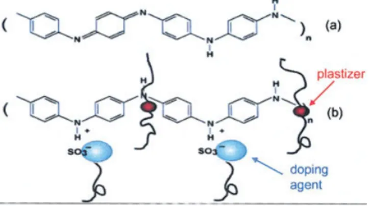
The chosen conducting polymer is polyaniline (PANI), as shown in Figure 1. The polyaniline used is chemically doped from the emeraldine base form. This process allows us to obtain a high level of conductivity. The company PANIPLAST provides it in solution form in dichloroacetic acid and formic acid. Like the majority of conducting polymers, polyaniline is not soluble; thus, we can talk about dispersion instead of a setting in solution. According to the quantities of various solvents used and the viscosity sought, conductivity can vary by one order of magnitude. Conductivity also depends on the process of evaporation of sol-vents; it can be selected on a range from 10 to 6000 S/m [7]. After drying the solution, we obtain a thin supple film of controllable
Figure 1 Polyaniline molecule: (a) polyaniline (emeraldine base and insulating form); (b) doped polyaniline (conductive form). [Color figure can be viewed in the online issue, which is available at www. interscience.wiley.com.]

![Figure 3 shows a comparison between the measured and cal- cal-culated S-parameters, for both our proposed method and the con-ventional method [5]](https://thumb-ap.123doks.com/thumbv2/9libinfo/7646775.138892/3.918.480.836.45.675/figure-comparison-measured-culated-parameters-proposed-method-ventional.webp)