TH6D-3
A V-Band GaAs
HEMT
Uniplanar Monolithic
Integrated Antenna and Receiver Front End
I-Jen Chen,
Huei
Wang, and Powen
Hsu
Department of Electrical Engineering and Graduate Institute
of
Communication Engineering
National Taiwan University, Taipei 106, Taiwan,
R.
0. C.
Tel: +886-2-23678315, Fax: +886-2-23651744
E-mail: [email protected]
Absfracf
-
A V-band monolithic integrated folded-slot balanced mixer with LO suurce on the same chip is presented for the first time. The circuit is designed based on the uniplanar structures such as coplanar waveguide (CPW) and slotline. The embedding impedance of the folded-slot antennais calculated by finite-difference time-domain (FDTD) method and compared with the impedance of the Schottky- Barrier diode at 60 GHz to design the mixer. The V-hand voltage control oscillator (VCO) is developed based on the
0.15 l m GaAs HEMT technology. A reduced-size CPW-to- slotline transition is designed for the LO pumping network. The measured results of the VCO, transition, and mixer are included.
I. INTRODUCTION
In recent years, the integrated antenna receiver has been used to replace traditional waveguide-based Schottky diode mixer to reduce the size, weight, and cost. Some quasi-optical mixers designed at various frequencies have previously been introduced [1]-[8]. A coupled slot antenna
was used in [ l ] and [2] to incorporate with a local oscillator (LO) source to form a self-contained receiver at X-band. A slot ring antenna loaded by two diodes formed a balanced mixer at X-band was presented in [3]. A folded-slot antenna was investigated
in [4]
and two diodes mounted in the slots of the antenna to provide mixing between the received RF and injected LO signals was shown in [SI at X-band. A slot and a twin-slot antennas were used with a matching network and a HFET or a diode to form the uniplanar receiver in [6] and [7] at 40 and 90 GHz, respectively. And a modified rectangular loop slot antenna was introduced to replace the twin-slot antenna at 65 GHz in[SI.
In these previous works [3]-[8], extemal LO circuits were used for the mixers. In [3], and [6]-[8], a waveguide hom was used to irradiate LO power to the mixers. This technique involves substantial loss of LO power. In[SI,
the LO signal was fed by a waveguide at X-band. Difficulties arise when one tries to feed LO power to the mixer at V-band from extemal LO source.07803-7695-1/03/$17.00 0 2003 E E E
In this work, the realization of a self-contained V-band monolithic integrated receiver which employs a folded- slot antenna and a balanced Schottky diode mixer with
HEMT VCO built on the same GaAs chip is presented.
Fmt, the embedding impedance of the folded-slot antenna is calculated by the FDTD method. The result is compared with the simulated impedance result of the diode to design the folded-slot balanced mixer. Then a VCO is designed based on 0.15 pm HEMT technology to provide the source of LO signal, using a similar circuit architecture reported in [9]. For the LO pumping network, a reduced-size CPW- to-slotline transition is designed based on the concept proposed in [lo]. The circuit schematic diagram is shown
in Fig. 1 . The circuit exhibits a 9.3 dBm output power of the VCO, 50 to 70 GHz bandwidth of the transition, and 18 dB isotropic conversion loss of the integrated folded- slot balanced mixer. The circuit is suitable for applications where compact size and light weight are required.
RFSlgnnl 59-610H2
m t c m Fig. 1.
receiver front end.
The schematic diagrani of the integrated antenna and
-
I d '
M
111. FOLDED-SLOT BALANCED MIXER DESIGN The architecture of the folded-slot balanced mixer is based on that described in
[SI.
Two diodes aTe mounted in the slots of the antenna to mix the LO signal injected from the slotline and RF signal received by the antenna. 2023The photo of the chip is shown in Fig. 2. The CPW-to- slotline transition can be seen in the middle of the figure,
where the VCO is on the left and the integrated folded-slot balanced mixer is on the right.
Fig. - 2. The chip Dhoto of the integrated antenna and receiver . . front end. Chip size is 3xl.5 mm2.
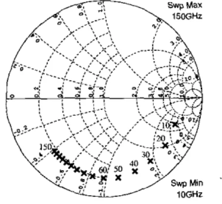
To begin the mixer design, the diode impedance is
simulated by the circuit design software Libra HP EEsof. The scaled model is used for the simulation of the two- finger 30 pm diode. The frequencies are swept form 10 to 150 GHz with 6 dBm LO power. The diode impedance can be read from the results in Fig. 3. At 60 GHz, the diode can be modeled as a RC parallel connection equivalent circuit, where R = 10 Q and C = 0.05 pF.
Fig. 3. Simulated diode impedance.
For
the feeding of LO power to the diodes,an
in-house FDTD program is written to calculate the return loss at the s l o t l i e input port. The CPW-fed folded slot antenna was previously analyzed by the FDTD method in [Ill . Similar program is developed and the lumped-element modeling technique in [I21 is applied here to calculate the return losses at the LO port by changing the positions of the diodes. Besides, the embedding impedances of the folded- slot antenna with diodes placed at different positions are also calculated for the RF signal matching consideration.The quasi-optical mixer [6]-[8] are mounted on the planar surface of a dielectric lens. Since the lens is
electrically large, the antenna elements act as if they are at the interface of an air-dielectric half-space. So the simulation environment is
a
half-space G a s substrate in which the antenna is printzd at the interface. From the simulation results, it is difficult to match the LO and RF signals to the diode at the same time. The length of the folded-slot antenna is chosen to be 1250 gm. Both the metal strip and the slot widths are 15 pm. Diodes are placed symmetrically about the LO feeding s l o t l i e and at the middle from center to cdge. The simulated results of retum loss and embedding impedance are shown in Figs. 4 and 5 , rcspectivcly.Slot Length (UL,)
Fig. 4. Simulated retum loss of LO input port.
-10
0.0 0.1 0.2 0.3 0.4 0.5 0.6
Slot Length (UL,)
Fig. 5. Simulated embedding impedance.
The IF frequency is 0.5 to 2.9 GHz, which
is
much lower than the RF frequency, so it is impractical to make a low pass filter (LPF) by waveguide sections as that presented in 151 on the chip. Instead, an on-chip LPF isimplemented by a 0.5 pF shunt capacitor.
#
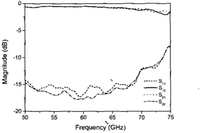
Fig. 7. The retum losses SI1 and S22 are more than IO dB from 50 to 70 GHz. The insertion losses S I I and S12 are
less than 0.7 dB in the same frequency band. 111. V-BAND VCO DESIGN
A V-band VCO is designed to provide the LO power on chip based on the same architecture and design procedure as those
in
[9]. In order to make the circuit accommodate to the balanced mixer structure, the VCO is designed on a grounded coplanar waveguide (GCPW) structure. The GCPW is used instead of CPW to prevent the LO signal from being injection-locked to the RF signal. A four- finger 200m
HEMT device is used. The oscillation frequency is adjusted by the gate bias voltage. The output power is coupled out o f the drain terminal via GCPW edge coupled lines. A Pi pad which causes 14 dB attenuation is implemented before the test port as an isolator. A test port is used here to test the VCO operating frequency and the output power. The test port will be left open when measuring the integrated antenna mixer, so an isolator is needed to suppress the influence. The coupler is designed to have a 6 dB insertion loss at LO port and 10 dB insertion loss at test port. All the passive structures are characterized by the full-wave EM analysis.IV. CPW-TO-SLOTLINE TRANSITION DESIGN
From the integrated antenna mixer design, the LO power is fed into the circuit from a slotline. From ,the VCO design, the output of VCO is a GCPW structure. So the GCPW is first mnsformed into CPW. Then a CPW-to- slotline transition is needed for the LO pumping network. To reduce the transition size, a planar parallel LC circuit composed of an interdigital capacitor and a shorted slotline stub is utilized to replace the conventional XI4 transformer structure [IO]. Based on the same design principle, the lumped-element CPW-to-slotline transition structure is implemented in V-band. The center frequency is designed at 60 GHz. To characterize the performance of such a transition, a test circuit consisting of the back-to- back connection of two such transitions is fabricated.
V. MEASUREMENT RESULTS
The chip is mounted on a 1.0 mm thick FR4 substrate
(E, = 4.3). The on chip VCO performance is measured from the test port by the probe station and spectrum analyzer. From the relationship between LO port and test port, the output power at LO port is known. The bias voltage is VD = 4 V and V , varies from 4 . 5 to 0.1 V. The oscillation frequency
is
about 62 GHz. Output power is about 8-9 dBm. The results are shown in Fig. 6. A phase noise of -78.28 dB/Hz for an offset frequency of 1 MHz is read from the spectrum analyzer. And the CPW-to-slotline transition test circuit is tested via on-wafer probing and network analyzer. Measured S-parameters are shown in20: 61.9 61.8
.
,.
I . ,.
, , . ,.
,.
1 2 4.6 4.5 -0.4 -0.3 4 . 2 4.1 0.0 0.1 0.2 Bias Voltage Vg (V) Fig. 6.LO port as functions of gate voltage.
The VCO oscillation frequency and output power at
-5
1
I
-204
.
,.
,
.
,50 55 60 65
ro
75\
Frequency (GHz)
Fig. 7. Measured S parameters of the CPW-to-slotline transition test circuit.
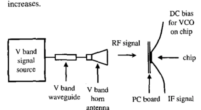
The integrated folded-slot balanced mixer is designed as a quasi-optical mixer mounted on a silicon dielectric lens. Because the lens is not available, the chip is preliminarily mounted on the FR4 substrate. Then a V-band standard gain horn antenna is used to irradiate the RF signal to the chip. The VCO
is
operating at62.0
GHz. The IF signal is picked out from the chip through the bond wires which connect the pads on the chip and the CPW line on the printed circuit board. An SMA connector and a coaxial cable are used to guide the IF signal from the printed circuit board to the s p e c r " analyzer. The setup is shown in Fig. 8. For simplicity, the definition of the isotropic conversion loss [l] is used to characterize the performance of the integrated folded-slot balanced mixer. Both the upper sideband and lower sideband isotmpic conversion\
losses are shown in Fig. 9. The conversion losses of both sidebands decrease fust to a m i n i u m level as the IF frequency increases and then increase as the IF frequency increases.
DC bias far
vco
I
onchipwaveguide horn PC board IF signal
antenna
Fig. 8. The mixer measurement setup for the integrated folded-slot balanced mixer.
35 I I Upper Sideband ,
. .
- . L w e r Sideband ,...
0.0 0.5 i . 0 1.5 2.0 2.5 3.0 IF Frequency (GHz) Fig. 9.lower sideband signal versui IF frequency.
The isotropic conversion losses of upper sideband and
VI. CONCLUSION
To the best of our knowledge, this circuit is the fust monolithic receiver that integrates an antenna and a mixer with a VCO built on the same chip. The chip has been designed and demonstrated at V-band. The circuit is compact and self-contained.
This receiver could
be mounted on a dielectric lens for millimeter-wave detector applications. It is suggested that several parameters of the antenna can be adjusted for RF signal matching to achieve further performance improvement.ACKNOWLEDGEMENT
,
This work is supported in part by the National Science Council, Republic of China, under contracts NSC 90- 2219-E-002-002 and NSC 90-2219-E-002-007, andin
partby the Ministry of Education, R. 0. C., under contract 89- E-FA06-2-4. The MMIC foundry service is provided by TRW Inc. through Chip Implement Center (CIC) in Taiwan. The authors would l i e to thank Ivir. Hong-Yeh Chang, Chun-Sian Lien, Kun-You Lin, Pei-Si Wu, and Dr. Hsin-Chia Lu for the suggestions and chip testing.
REFERENCES
[I1 V. D. Huang, T. Uwano, and T. Itoh, “Quasi-optical integrated antenna and receiver front end,’’ [EEE Trans. Microwave Theory and Tech., vol. Mm-36, no. I, pp. 80-
85, Jan. 1988.
121 V. D. Huang, and T. Itoh, “Quasi-optical HEMT and MESFET self-oscillating mixers,’’ IEEE Trans. Microwave
Theory and Tech., vol. M7T-36. no. 12, pp. 1701-1705, Dec. 1988.
131 S . K. Masanveh, T. N. Sherer, K. S. Yngvesson, R. L. Gingras, C . Drubin, A. G . Cardiasmenos, and 1. Wolverton, “Modeling of a monolithic slot ring quasi-optical mixer,”
IEEE Trans. Microwave Theory and Tech., vol. Mll-42, no. 9, pp. l&l2-l6G9, Sep. 1994.
141 S. V. Robertson, N. I. Dib. G. Yang, and L. P. B. Katehi. “A folded slot antenna for planar quasi-optical mixer applications,” 1993 IEEE AP-S Dig., pp. 600-603.
[ 5 ] S. V. Robertson, L. P.
B.
Katehi, and G. M. Rebeiz, “A planar quasi-optical mixer using a folded-slot antenna,”IEEE Trans. Microwave Theory and Tech., vol. MTl-43, 161 H. H. G . Zirath, C . Y. Chi, N. Rorsman, and G. M. Rebeiz, “A 40-GHz integrated quasi-optical slot HFET mixer,”
IEEE Trans. Microwave Theory and Tech., vol. MTI-42, no. 12, pp. 2492-2497, Dec. 1994.
171 G. P. Gauthier, W. Y. Ali-Ahmad, T. P. Budka, D. F. Filipovic, and G. M. Rebeiz, “A uniplanar 90-GHz Schottky diode millimeter-wave receiver,” IEEE Truns. Microwave Theorj and Tech., vol. M1T-43, no. 7, pp, 1669-1672, July 1995.
[RI
P. Otero, G. V. Eleftheriades, and I. R. Mosig, “Integrated modified rectangular loop slot antenna on substrate lenses for millimeter- and submillimeter-wave frequencies mixer applications,” IEEE Trans. Microwave Theory and Tech., vol. MTT-46, no. 10, pp, 1489-1497, Oct. 1998.191 H. Wang, K. W. Chang, T. H. Chen, K. L. Tan. G . S. Dow,
B.
Allen, and J. Berenz, “Monolithic W-hand VCOs usingpseudomorphic AlGaAs/lnCaAs/GaAs HEMTs,” 1992
IEEE GaAS IC Symp. Dig., pp. 47-50.
[lo] Y. S . Lin, and C .
H.
Chen, “Novel lumped-element uniplanar transitions,” IEEE Trans. Microwave Theory undTech., vol. MTT-49, no. 12, pp. 2322-2330, Dec. 2001. [ I l l H. S. Tsai, and R. A. York, “FDTD analysis of CPW-fed
folded-slot and multiple-slot antennas on thin substrate,”
IEEE Trans. Antennas Propagat.. vol. 44, nu. 2, pp. 217- 226, Feb. 1996.
1121 A. Taflove, Computational Electrodynamics
-
The Finite- Difference Time-Domain Method, Boston: Artech House,1995.