A CMOS BPSK Transmitter with a Monitoring Demodulator
Embedded
Hung-Chi Wang#1, Jyh-Ching Juang#2, Chun-Lin Lu*3
#Department of Electrical Engineering, National Cheng Kung University No.1 Ta-Hsueh Road, Tainan 701, Taiwan, R.O.C.
1n2896113@mail.ncku.edu.tw
2juang@mail.ncku.edu.tw
*Department of Computer and Communication, Kun Shan University No.949, Da Wan Rd, Yung-Kang City. Tainan Hsien, Taiwan, R.O.C.
3cllu@mail.ksu.edu.tw Abstract — A binary phase shift keying (BPSK) transmitter
with a monitoring demodulator embedded using standard 0.13- µm CMOS process is presented in this paper. Three differential switches, an RF multiplexer and a sub-harmonic VCO are applied in the circuit design. The differential switches offer the frequency-doubling function for VCO, the modulation function for the transmitter, and the demodulation function for the monitor. The measurement results show that the free-running frequency of the VCO of the chip is around 11 GHz and the doubled frequency is around 22 GHz. A continuous-wave signal is applied to test the transmitter function. The measured results show that the modulator bandwidth is wider than 3 GHz. The LO-to-RF isolation is better than 55 dB. The monitor circuit is tested to show that un-wanted signal will appear if the quality of the transmitted signal is poor. The chip size is 1 × 1 mm2.
Index Terms — BPSK, CMOS, monitoring, transmitter.
I. INTRODUCTION
Recently, the rising demand of high-speed transmission data rates of wireless applications has driven the technology development of the next-generation communication systems [1-4]. Federal Communications Commission (FCC) has allocated several frequency spectra to accommodate the operation of these new devices. Commercial applications such as high-definition multimedia streaming, the point-to- point links require multi-gigabit data transmission. Wireless transmission of high-definition multimedia streaming from several high-definition cameras is required in order to avoid large delay times. Thus, there is a need for multi-gigabit wireless technology that can support regulation standards and transmit multiplexed high-definition multimedia streaming operating at gigahertzes. With the increase in the complexity of the modulation scheme, there are significant and rising challenges in the analog demodulation techniques. Numerous attempts have been made by scholars to demonstrate wireless front-end research [5-9] for the millimeter-wave region, and can handle multi-gigabit data rates. Unfortunately, there are rare article to demonstrate that has provides circuit to detect the modulated data signal correctness for multi-gigabit wireless technology. In this paper, a millimeter-wave CMOS BPSK transmitter with monitoring demodulator embedded technique is presented. The baseband data signal correctness could be detected directly for high speed data rates system application. This paper is organized as follows. First, in Section II, the BPSK transmitter architecture is introduced.
Each circuit block is depicted in section III. Demonstration of
the BPSK transmitter is characterized in section IV. Finally, concise conclusions are drawn in section V.
II. TRANSMITTER ARCHITECTURE
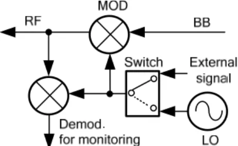
In this paper, a BPSK transmitter with monitoring demodulator embedded is presented as shown in Fig. 1. This chip employed two differential switches [10] to similar a Gilbert cell mixers [11-13] to demonstrate up-conversion modulator and demodulator to confirm baseband data correctness before transmitted. The chip also employed one differential switch for a sub-harmonic VCO of pumping technique. One RF multiplexer is applied between local- oscillator (LO) and differential switches for selecting internal or external LO signals to increase the testability.
Fig. 1. Block diagram of the proposed transmitter.
III.CIRCUIT DESIGN
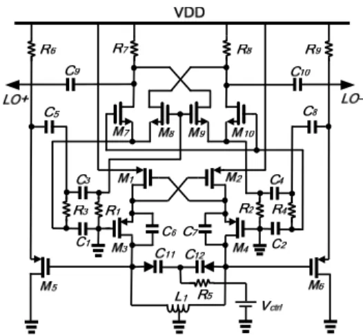
This BPSK transmitter is fabricated using TSMC commercial standard 0.13µm 1P8M CMOS process, which provides one ploy layer for the gates of CMOS transistors and eight metal layers for inter-connection. The modulator and sub-harmonic VCO with monitoring demodulator is employed in this circuit design. The structure of the differential switches operates as a mixer as shown in the Fig.
2. The selection of the switches size is tradeoff between the output power and translation speed. Fig. 3 shows the schematic of sub-harmonic VCO, which consists of two RC- CR circuits, a differential switches, and a 11GHz differential Colpitts VCO. The schematic of modulator with monitoring demodulator is shown in the Fig. 4, which consists of two differential switches, a current mode switches. The Design of those circuits is described as the follows:
A. The differential switch
The differential switch is used not only as a frequency doubler but also the phase modulator. Fig. 2 shows the schematic and the symbol of the differential switch [10]. It consists of four NMOS and is organized to be two-input (in, in_b), two-output (out, out_b), and two control terminals (Vc, Vc_b). Fig. 2(b) shows the symbol of the differential switch where the arrows indicate the direction of the internal current flow. Here the current flows from the output terminal to the input terminal in most applications. When the control voltage is relatively “low”, or in other words, (low, high) or (0,1) voltage signals are applied to the (Vc, Vc_b) terminals, the differential switch will stay in OFF state. M1 and M2 are both in ON state and appear to be short, while M3 and M4 are both in OFF state and appear to be open. Hence, the input terminals are connected straight to the output terminals without exchange in this situation. The working principle is similar but the terminals are exchanged while the control voltage is relatively “high”.
Fig. 2. The differential switch (a) the schematic (b) the symbol.
B. Sub-harmonic Colpitts voltage control oscillator
Fig. 3 shows a schematic of proposed Colpitts VCO. Only PMOS transistors are used in the circuit. It consist PMOS cross-coupled pair of a current-switch pair (M1 and M2) to provide the negative resistance for the start-up condition.
Also there are two symmetrical single-ended Colpitts VCO (M3 and M4) which is individually connected to a varactor diode (C11 and C12). In the proposed circuit, the differential pair is connected to VDD node directly for the trade-off of the chip size and the output swing. Without the transistor constant current source, the bias current was directly controlled by choosing the transistor size. In order to fit the condition of the differential Colpitts oscillator, one on-chip symmetrical inductor (L1) with a center-tap is inserted in VCO as the tank circuit. A sub-harmonic frequency doubler is a circuit which converts signals from low frequency to twice of the original frequency. It consists of two RC-CR (R1, R3, C1, C3 and R2, R4, C2, C4) circuits, buffers, and a differential switch (M7-M10). Two RC-CR circuits are attached immediately after the 11-GHz VCO to split the complementary signals into four orthogonal phases. Here assumes that the original signals before the frequency doubler are large enough to turn the transistors of the differential switch into saturation state. With the self-mixing of the same signal but quadrature phase difference via the differential switch that exactly 90 degree phase difference between the RF and LO input signals will let the differential switch to output the maximum power of the doubled signal, and the working frequency will be doubled up to 22 GHz.
Fig. 3. Schematic of the sub-harmonic VCO.
C. BPSK Modulator with monitoring demodulator
Fig. 4 shows the schematic of the modulator with monitoring demodulator embedded. The differential switches are used as a phase modulator (M5-M8) at the baseband (BB) port and demodulator (M9-M12) which is between the LO and RF port. The working principle is the signal connected at the input terminal of the switch will be bypassed to the output terminal if the control voltage is low. Reversely the output signal will be exchanged if the control voltage is high. The RF multiplexer (M1-M4) which consists of four bias resisters (R1 - R4) are employed for selecting the internal LO or external input signal to enhance the chip testability. LO signal is modulated in the phase modulator by the CW baseband signal data, and demodulated by demodulator, to confirm data correctness for high speed data rates system application. The capacitors (C1 - C8) and resisters (R5 - R10) are used as dc block and loaded respectively.
Fig. 4. Schematic of the modulator with monitoring demodulator.
IV.IMPLEMENTATION AND MEASUREMENTS
The measurements of the BPSK transmitter chip were performed via on-wafer probing. The isolation of the chip were measured by using Rohde & Schwarz ZVA vector network analyzer, and the measured LO-to-RF and LO-to- baseband isolations versus LO frequency are shown in Fig. 5.
Form 15 to 40 GHz, the port-to-port isolation is better than
55dB. High isolation is necessary for the applications of the high modulation/demodulation quality due to the dc offset issue. For the modulation and demodulation measurement, the baseband signals are generated by using Rohde &
Schwarz SMV100A vector signal generator. A Rohde &
Schwarz FSP spectrum analyzer is used for modulated RF and demodulated baseband output spectrum measurement.
The measured spectrum of VCO is shown in Fig. 6. Two spectrums, allocated at 10.9 GHz and 21.9 GHz respectively, are found. It means the VCO is working at 10.9 GHz and the frequency doubler mixes the signal up to 21.9 GHz. The measurement of the free running phase noise is –107 dBc/Hz at 1-MHz offset from a 10.7-GHz carrier, which shown in Fig. 7. In Fig. 8, shows the output spectrum of the phase modulator under the condition that the phase modulator is connected to the output of the frequency doubler (21.5 GHz) with a LO power of 10 dBm and a CW baseband analog signal of 3 GHz in this test. The measurement result shows that two spectrums, allocated around 18.5 GHz and 24.5 GHz respectively, are generated. It certifies that the phase modulator is functional work with 3-GHz channel bandwidth.
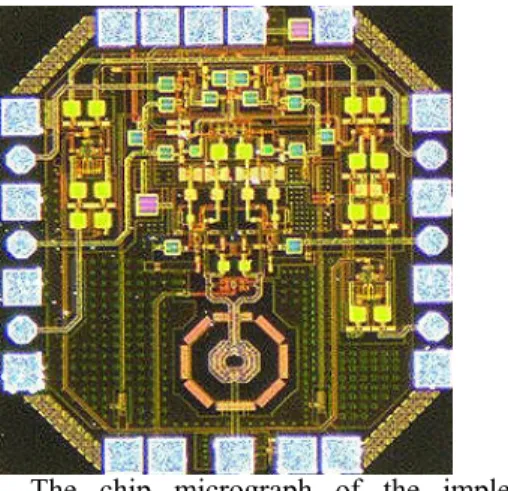
Fig. 9 shows the measured output spectrum of demodulation data at 3 GHz without error data signals. The measured output spectrum of demodulation data with the error data signal at 3.155 GHz has been detected by monitoring demodulator, which as shown in Fig. 10. The VCO core and modulator with current mode switch dissipate 5mW and 20mW respectively. The chip micrograph with a die area of 1
1 mm2 is shown in Fig. 11.Fig. 5. Measured port-to-port isolation of the modulator.
Fig. 6. The measurement of the output spectrum of VCO.
Fig. 7. Fig. 5. Measured free running phase noise.
Fig. 8. Measured output spectrum of modulator at 22GHz with continue-wave of 3 GHz.
Fig. 9. Measured output spectrum of demodulation signals at 3 GHz.
Fig. 10. Measured output spectrum of demodulation signal of 3 GHz with error signal at 3.155 GHz.
Fig. 11. The chip micrograph of the implemented transmitter.
V. CONCLUSIONS
An architecture of a BPSK transmitter with monitoring demodulator embedded is proposed. The chip is implemented in TSMC 0.13-um CMOS process. Three Differential switches, a current mode switches and a sub-harmonic VCO pumping technique is applied in the circuit design. The differential switches are employed in the transmitter for the purposes of the frequency doubling and phase modulator and applied to confirm data signal correctness as monitoring demodulator. The free-running frequency of the VCO drifts to around 11 GHz, hence the doubled frequency drifts to around 22 GHz. The up-conversion phase modulator is measured to be successful. It is connected by the doubled frequency (around 21.5 GHz) and an external CW baseband signal at 3-GHz. The measured spectrum of the modulator output found two spectrums of around 18.5 GHz and 24.5 GHz. It certifies that the phase modulator is functional work with 3-GHz channel bandwidth. In addition, the measured output spectrum of demodulation data with the error signal at 3.155 GHz has been detected by monitoring demodulator.
The total current consumption of the modulator with current mode switch and core of VCO is 21.2mA with a dc supply voltage VDD of 1.2 V. The chip size is 1
1 mm2.ACKNOWLEDGEMENT
The authors would like to thank the Chip Implementation Center (CIC) of the National Science Council, Taiwan, ROC, for supporting the TSMC CMOS process.
REFERENCES
[1] Y. –H. Kao; W. -Y. Chen, “SAW oscillator based clock recovery for high speed serial data transmission,” Asia-Pacific Microwave Conference, 2008, pp.1-4.
[2] A. Tanaka, H. Okada, et al., “A 1.1V 3.1-to-9.5GHz MBOFDM UWB Transceiver in 90nm CMOS”, IEEE ISSCC Dig. Tech. Papers, p.398-407, Feb., 2006.
[3] D. Yeh, S. Sarkar, et al., “An Integrated IQ Demodulator with Integrated Low-Power Multi-Gigabit BPSK/ASK Analog Signal Processor in 90nm CMOS”, IEEE EuMIC, pp.139-142, Oct., 2008.
[4] S. Chakraborty; U. –D. Kumar; S. Panda; B. Gupta; K.
Yasumoto,“Parasitically loaded broad band microstrip antennas
for proposed IEEE 802.15.3a (UWB) communication systems,”
Asia-Pacific Microwave Conference, 2006, pp.1983-1986.
[5] C. –H. Hu, H. –L. Wu, C. –Y. Chang, S. –J. Chung, “A wireless video relay system at 28 GHz”, Asia-Pacific Microwave Conference, 2001, pp.617-620.
[6] H. Tsuji, H. Ogawa, M. Hirakawa, “An alternative high-speed wireless access system with mobile tracking technology”, Asia- Pacific Microwave Conference, 2000, pp.634-637.
[7] K. -C Choi, D. Kim, M. Ko, W. –Y. Choi, “1-Gb/s mixed- mode BPSK demodulator using a half-rate linear phase detector for 60-GHz wireless PAN applications”, Solid-State Circuits Conference, 2008, pp.357-360.
[8] Y. –H. Chen, H. –H. Hsieh, L. –H. Lu, “A 24-GHz Receiver Frontend with an LO Signal Generator in 0.18-μm CMOS,”
IEEE Trans. Microwave Theory & Tech., vol. 56, pp.1043- 1051, May 2008.
[9] W. C. Wang; C. Y. Wu, “The 1-V 24-GHz low-voltage low- power current- mode transmitter in 130-nm CMOS technology,” IEEE Microelectronics and Electronics Conference , pp. 49-52, July 2007.
[10] C. -L. Lu, H. -C. Wang, J. -C. Juang, and H. -R. Chuang, “10- Gb/s CMOS Ultrahigh-Speed Gold-Code Generator Using Differential-Switches Feedback”, EuMIC2007, pp. 239-242, Munich, Germany, Oct. 8-9, 2007.
[11] G. K. W. Hamed, A. P. Freundorfer, Y. M. M. Antar, P. Frank, and D. Sawatzky, “A high-bit rate ka-band direct conversion QPSK demodulator,” IEEE Microw. Wireless Compon. Lett., vol. 18, no. 5, pp. 365–367, May 2008.
[12] J.-H. Tsai and T.-W. Huang, “35–65-GHz CMOS broadband modulator and demodulator with sub-harmonic pumping forMMWwireless gigabit applications,” IEEE Microw. Theory Tech., vol. 55, no. 10, pp. 2075–2085, Oct. 2007.
[13] P. Lindberg, E. Ojefors, E. Sonmez, and A. Rydberg, “A SiGe HBT 24 GHz sub-harmonic direct-conversion IQ- demodulator,” in Proc. Topic Meeting Silicon Monolith. Integr.
Circuits RF Syst., Sep. 8–10, 2004, pp. 247–250.
[14] R. M. Kodkani, L. E. Larson, “A 24-GHz CMOS Passive Subharmonic Mixer/Downconverter for Zero-IF Applications,”
IEEE Trans. Microwave Theory & Tech., vol. 56, pp. 1247- 1256, May 2008.
[15] R. M. Kodkani, L.E. Larson, “A 24-GHz CMOS Direct- Conversion Sub-Harmonic Downconverter,” IEEE RFIC Symp.
Dig., pp. 485-488, June 2007.
[16] B.G. Perumana, C. –H. Lee, J. Laskar, S. Chakraborty, “A subharmonic CMOS mixer based on threshold voltage modulation,” IEEE MTT-S International Microwave Symp.
Dig., pp. 33-36, June 2005.
[17] X. -G Yang, J. -S Lin, “Design and Analysis of a Low-Power Discrete Phase Modulator in a 0.13-_m Logic CMOS Process,”
IEEE Microw. Wireless Compon. Lett., vol. 16, no. 3, pp. 137- 139, March. 2006.