Characterization of InGaN
Õ
GaN multi-quantum-well blue-light-emitting
diodes grown by metal organic chemical vapor deposition
K. S. Ramaiah,a)Y. K. Su, S. J. Chang, and B. Kerr
Department of Electrical Engineering, National Cheng Kung University, Tainan 701, Taiwan ROC
H. P. Liu and I. G. Chen
Department of Materials Science and Engineering, National Cheng Kung University, Tainan 701, Taiwan ROC
共Received 5 December 2003; accepted 9 March 2004兲
The structural, surface morphology, and the temperature dependence photoluminescence of InGaN共3 nm兲/GaN共7 nm兲 5 period multi-quantum-well blue-light-emitting diode 共LED兲 structures grown by metal organic chemical vapor deposition共MOCVD兲 have been studied. Quantum dot-like structures and strain contrast evident by black lumps were observed in the quantum wells using high-resolution transmission electron microscopy 共HRTEM兲 analysis. Double-crystal high-resolution x-ray diffraction共HRXRD兲 spectra of blue LED were simulated using kinematical theory method, to obtain composition, and period thickness of well and barrier. The ‘‘S’’ shape character shift as red–blue–redshift of the quantum-well emission line, i.e., blue emission peak 2.667 eV at 10 K, was observed with variation of temperature in the photoluminescence 共PL兲 spectra. The shift is assigned to the potential fluctuations due to alloy inhomogeneous distribution in the quantum wells. The In composition in the quantum wells obtained by two independent techniques, namely HRXRD and PL, was 8% and 19%, respectively. The reason for this large difference in composition is explained in this letter. © 2004 American Institute of Physics. 关DOI: 10.1063/1.1728302兴
Nitride-based blue and green light-emitting diodes illu-minating with high brightness are now commercially avail-able, despite high dislocation density of 108– 109 cm⫺2 in the epilayers.1 The InGaN/GaN multi-quantum-well struc-tures are being used as active layers in the light-emitting diodes共LED兲 because the emission spectrum can be tailored from ultraviolet to visible region by varying In composition. The blue LEDs, which showed higher efficiency than that of green LEDs, have been widely used in the communication and information technologies. The In mole fraction of 0.1– 0.2 and 0.45 is required for blue and green LEDs, respec-tively. The phase separation or segregation of In is a major problem in the InGaN system due to solid phase immiscibil-ity between InN and GaN. This segregation is due to a large difference in interatomic spacing, and other physical proper-ties such as thermodynamical and chemical instabiliproper-ties, etc., which are very different between InN and GaN. The experi-mental and theoretical studies revealed that the solid-phase immiscibility is high in InGaN.2At normal growth tempera-tures, the alloy is unstable over the entire composition. The formation of phase separation leads to a quantum dot-like structure, which is highly beneficial to obtain high external quantum efficiency from the InGaN/GaN LEDs structures.3 Due to a lack of understanding of this phase segregation, LED structures have to be investigated with respect to struc-tural, optical properties, etc., to know the role of In in the wells.
The blue LEDs studied were prepared on c-plane
sap-phire substrates by using conventional MOCVD technique. The GaN buffer layer with thickness of 25 nm was grown at a low temperature of 560 °C, followed by 2 m thick Si-doped GaN layer at a higher temperature of 1060 °C, on which a 5 period of 3 nm InGaN well共W兲/7 nm GaN barrier 共B兲 was grown at a temperature of 780 °C using N2only as a
carrier gas. This structure was capped with p-GaN having a thickness of 0.5 m. Trimethyl-gallium, trimethyl-indium, and NH3 were used as precursors for Ga, In, and radical
nitrogen, respectively. N2 and H2 were chosen as carrier gases to grow layers. The entire deposition process was de-scribed in detail elsewhere.4
The samples were mechanically polished and then thinned by employing Ar⫹ laser to study their microstruc-tures. Philips transmission electron microscope was operated at 200 kV to obtain structural data. Crystal structure was characterized using a Philips X-pert double-crystal x-ray dif-fractometer with Ge 共220兲 single crystal, operated at 40 kV and 50 mA with radiation of 1.540 56 Å. Nanoscope atomic microscope was used to scan the surface of the LED struc-ture. For PL measurements, a He–Cd laser operated at 325 nm, a GaAs-based photodetector used to record excited emission, and a closed-loop He cryostat for low temperature were employed.
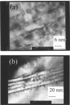
AFM analysis showed the root-mean-square 共rms兲 sur-face roughness of 1 nm of the quantum well sample. TEM analysis revealed that an average width of the period was found to be 10.2 nm, i.e., well width ⬃3 nm and barrier width ⬃7.2 nm from a micrograph. Figure 1共a兲 shows dark contrast regions formed between the intermixing of InGaN quantum wells and GaN barriers by relaxation of strain, known as strain contrast. The quantum dot-like structures are a兲Present address: Department of Electrical Engineering, Virginia
Common-wealth University, 601 W. Main St, Richmond, VA 23284; electronic mail: [email protected]
APPLIED PHYSICS LETTERS VOLUME 84, NUMBER 17 26 APRIL 2004
3307
0003-6951/2004/84(17)/3307/3/$22.00 © 2004 American Institute of Physics
clearly visible in the well regions but not in the barriers, as shown in Fig. 1共b兲. The formation of quantum dot-like struc-ture in the InGaN multiquantum well is evident due to the low miscibility of InN in GaN.
The experimental/2XRD scan for LED structure was simulated by using the kinematical theory method, which gave an approximate average indium composition of 8% in the wells, as shown in Fig. 2. Surprisingly, PL analysis indi-cated an In composition of⬃19% in the wells. The anoma-lous behavior could be a quantum-confined Stark effect 共QCSE兲5
due to piezoelectric field caused by strain between well and barrier. In general, the intense PL emission is pro-vided by the quantum dot-like structures, which have effi-cient radiative recombination centers when compared to the usual layers. The In-rich GaN matrix favors longer wave-length emission, whereas XRD analysis showed an
approxi-mate average In composition in the well layers giving a lower value. Tran et al.6also observed that In composition in the multiquantum well structures is less than that in the in-dividual or usual InGaN layers. The width of the period共well and barrier兲 was determined to be 10 nm by using the simple relation n/关2(sini⫺sinj)兴, where is the wavelength of x-ray radiation, i, j are angles of the adjacent i and j satellite peaks, and n is the order between the adjacent sat-ellite peaks of i and j . The occurrence of well-resolved sharp diffraction or satellite peaks indicates that the interface be-tween well and barrier is abrupt; however, the right-hand-side satellite peaks are less pronounced, which is common in quantum well structures because the periods are not in phase and unequal in compositions at micro levels. In the case of green LEDs, satellite peaks are less pronounced due to high-In composition fluctuations in the layers.
In order to obtain blue emission共BL兲 at 465 nm 共2.667 eV兲 from the LEDs, the required In mole fraction in the quantum well structures is 0.2. Recent results confirmed that the band gap of InN is ⬃0.77 eV with a bowing parameter determined to be 1.43, as shown in the equation,7 Eg(x) ⫽3.42x⫹0.77(1⫺x)⫺x(1⫺x)1.43. The band gap 共Eg兲 of InGaN can be calculated from the InGaN quantum-well ground-level emission (E1e1h) i.e., blue emission peak at 2.667 eV, using the relation E1e1h⫽Eg⫺eFWLW
⫹(9បeFW/8冑2)2/3((1/me)⫹(1/mh))1/3. From these rela-tions, In composition in the InGaN wells was found to be ⬃19%, which is not necessarily equal to that of XRD results because the QSCE could be involved in the quantum-well emission, unlike absorption measurements; thus, the In com-position obtained from the PL measurements might be larger than that of XRD measurements. The emission peak showed ‘‘S’’-shape character shift, as temperature decreased from room temperature to 10 K and two phonon 共LO兲 replicas existed with energy difference of about 91 meV, as shown in Fig. 3. The other emission peaks such as band edge emission 共BE兲 at 3.469 eV, donor acceptor pair 共DAP兲 at 3.285 eV, and its 共phonon兲 replicas pronounced at 3.192, 3.099, and 3.008 eV with a difference of about 91 meV and yellow band共YB兲 emission at 2.214 eV, which are mainly from GaN. The S-shape character shift is due to potential fluctuations caused by inhomogeneous compositional and interface fluctuations in the quantum-well structures. As temperature increased
FIG. 1. Transmission electron micrographs of quantum-well structure:共a兲 high-resolution transmission electron micrograph bright field images, show-ing well and barrier width of 10.2 nm, black contrast resultshow-ing in strain between the well and barrier regions, and共b兲 quantum dot-like structures very clearly visible in the well regions.
FIG. 2. Double-crystal x-ray diffraction spectrum/2scan of the InGaN/ GaN multi quantum-well blue LED structure:共a兲 Experimental 共solid line兲 and共b兲 Simulation 共dashed line兲, giving In composition of 8% in the wells.
FIG. 3. PL spectra of the InGaN/GaN multi-quantum-well blue LED struc-ture measured at different low temperastruc-tures; the quantum-well peak shows ‘‘S’’ shape character shift red–blue–redshift with variation of temperature.
3308 Appl. Phys. Lett., Vol. 84, No. 17, 26 April 2004 Ramaiahet al.
from 10 to 60 K, the peak showed redshift with respect to photon energy because the 共electron hole pairs兲 carriers, which are randomly distributed in the potential minima at low temperature, do not have sufficient thermal energy so that they relax down to lower energy level states by reducing higher energy emission. As temperature further increased 共80–140 K兲, the emission peak showed blueshift, indicating the carriers do have sufficient thermal energy to occupy higher energy level states by emitting higher energy radia-tion. For the temperature range of 160–303 K, there is again redshift, which is commonly accepted to be due to nonradi-ative recombination rates, which dominate radinonradi-ative recom-bination rates at room temperature.8,9 We observed that the PL intensity of quantum wells without a capping layer was higher than that of p-GaN capped quantum-well structures because there is intraband absorption in the capped layer.10 The PL quantum efficiency and full width at half maximum of the QW peak for the LED structure were found to be 0.05% at room temperature and 62 meV at 10 K. The blue emission peak intensity versus inverse temperature gave the activation energy of 43 meV, indicating the localization of the carriers in the structure. The activation energy was in-creased with increasing In composition, resulting in deep lo-calization energies of excitons due to potential fluctuations.11 However, PL quantum efficiency is higher in the blue LEDs as compared to that in the green LEDs, which is due to domination of stronger intrinsic radiative recombination rather than nonradiative recombination. The decrease of PL intensity with increasing temperature can be attributed to the thermionic emission of the excited photocarriers due to po-tential fluctuations, which arise from the compositional fluc-tuations in the well and also from the interface roughness fluctuations between well and barrier.
In conclusion, the essence of the results is that the strain, quantum dot-like structures, and the widths of well and bar-rier were observed from TEM analysis for blue LEDs. AFM
analysis showed rms roughness of 1 nm resulting in good quality of the layers. The low-temperature PL studies showed that ‘‘S’’-shaped character shift, i.e., red–blue–redshift of quantum-well emission is attributed to the potential fluctua-tions due to alloy inhomogeneity and interface roughness in the quantum wells. The higher activation energy of 43 meV is indication of deep localization energies of excitons.
The authors would like to thank National Science Coun-cil共NSC兲 Taipei, for partial financial support under Contract No. NSC 85-2215-E-006-004. We thank Professor H. Morkoc¸ and Professor D. Johnstone for fruitful discussions.
1
S. Nakamura and S. F. Chichibu, Introduction to Nitride Semiconductor
Blue Lasers and Light Emitting Diodes共Taylor & Francis, New York,
2000兲.
2K. Jacobs, B. Van Daele, M. R. Leys, I. Moerman, and G. Van Tendeloo,
J. Cryst. Growth 248, 498共2003兲.
3
N. Grandjean, B. Damilano, J. Massies, and S. Dalmasso, Solid State Commun. 113, 495共2000兲.
4K. S. Ramaiah, Y. K. Su, S. J. Chang, F. S. Juang, and C. H. Chen, J.
Cryst. Growth 220, 405共2000兲.
5
S. F. Chichibu, A. C. Abare, M. P. Mack, M. S. Minsky, T. Deguchi, D. Cohen, P. Kozodoy, S. B. Fleischer, S. Kell, J. S. Speck, J. E. Bowers, E. Hu, U. K. Mishra, L. A. Coldren, S. P. DenBaars, K. Wada, T. Sota, and S. Nakamura, Mater. Sci. Eng., B B59, 298共1999兲.
6C. A. Tran, R. F. Karlicek, Jr., M. Schurman, A. Osinsky, V. Merai, Y. Li,
I. Eliashevich, M. G. Brown, J. Nering, I. Ferguson, and R. Stall, J. Cryst. Growth 195, 397共2001兲.
7M. C. Johnson, R. J. Jogerson, J. Wu, W. Shan, and E.
Bourret-Courchesne, J. Cryst. Growth 261, 44共2004兲.
8K. S. Ramaiah, D. Huang, M. A. Reshchikov, F. Yun, H. Morkoc,
J. Jasanski, Litilental-Weber, S. C. Sone, and S. H. Park, J. Mater. Sci.: Mater. Electron. 11, 239共2003兲.
9Y. Han, H. Chen, H. B. Yu, D. S. Li, Z. B. Yan, Q. Huang, and J. M. Zhou,
J. Cryst. Growth 253, 203共2003兲.
10
Q. Zhou, J. Chen, B. Pattada, M. O. Manasreh, F. Xiu, S. Puntigan, L. He, K. S. Ramaiah, and H. Morkoc¸, J. Appl. Phys. 93, 10140共2003兲.
11K. L. Teo, J. S. Colton, P. Y. Yu, E. R. Weber, M. F. Li, W. Liu, K. Uchida,
H. Tokunaga, N. Akutsu, and K. Matsumoto, Appl. Phys. Lett. 73, 1697
共1998兲.
3309 Appl. Phys. Lett., Vol. 84, No. 17, 26 April 2004 Ramaiahet al.