i
國立臺灣大學理學院物理學系 碩士論文
Department of Physics College of Science
National Taiwan University Master Thesis
鎳、鈷薄膜在鈀/鵭(111)表面之吸附與縐化現象 Adsorption and faceting phenomenon of Ni, Co thin
films on Pd / W(111) surface
忻佳緯 Xin, Jia-Wei
指導教授:宋克嘉 博士、張嘉升 博士
Advisor: Ker-Jar Song, Ph.D.,Chia-Seng Chang, Ph.D.
中華民國99 年 7 月 July, 2010
ii
iii
誌謝
首先感謝宋克嘉老師給我這個機會接觸表面物理這個領域。宋老師總是能在 我碰到瓶頸時指引我走向正確的方向,而且能一步步引導我加深對物理這門學科 的認識,同時也常常在私底下跟我分享他的人生歷鍊。他追求科學的態度往往讓 我感佩。此外也要謝謝黃昶翰,他的研究成果是本次研究的基盤,也在實驗過程 中提供了我許多技術上的建議,沒有他的幫助我的實驗將會困難重重。還要謝謝 嚴亮宇,有你們兩個在是我會進這個實驗室的原因之一。
接下來要感謝黃仲祥學長,常常來關心我的實驗進度,和我一起討論實驗結 果並指出我推論中的錯誤。還有實驗室裡的同學張智翔,總是能在我感到疲憊困 頓的時候幫我加油打氣,也提供了我生活中的許多樂趣。另外謝謝劉冠德學長,
提供了我撰寫論文的許多建議,他認真負責的態度是我學習的目標。
最後要感謝我的家人,在我讀碩士班的過程中提供經濟上的支持,同時成為 我精神上的支柱,讓我可以順利完成研究所的學業。
iv
中文摘要
在本研究中我們探討了鎳、鈷簿膜在鈀/鵭{112}縐化表面之熱穩定性與熱 動力學特性。我們發現在熱退火後鎳和鈷都會與鈀在表面形成合金,而令人驚訝 的是,其中鎳可以幫助鈀在鎢(111)表面引發縐化現象。另外 11 個熱脫附單層的
鈷和1.2 個熱脫附單層的鈀薄膜在熱退火後的低能量電子繞射圖形只顯示出相當
微弱的{112}面繞射點,且沒有原先(111)面的繞射點。程控溫歐傑電子能譜顯示 大於一個熱脫附單層的鈷、鎳薄膜在熱處理過程中均會形成三維島狀結構,表示 這些較厚的膜在縐化表面並不是穩定的,而不能作為製備磁性單原子針尖的方法。
但從這些實驗中我們發現小於一個熱脫附單層的鎳薄膜在(鎳,鈀)/鎢(111) 表面具有良好的熱穩定性,這些系統仍有相當的潛力且值得在未來做更進一步的 磁性量測。
v
Abstract
We studied the thermal stability and thermodynamic properties of Ni, Co ultra thin films on faceted Pd/W{112} system. We found that both Ni and Co will form alloy with Pd upon annealing. To our surprise, the Ni is able to “help” Pd in inducing the faceting of W(111) surface. As for Co, after deposition and annealing of up to 11 TML of Co on 1.2 TML of Pd, faint LEED spots from {112} faceted surface always persist on top of a diffuse background, while no LEED spots from planar (111) surface is ever observed. Temperature programmed Auger spectra show thick films (>1TML) of Co and Ni tend to form 3D islands on the faceted surface upon annealing, indicating such uniform thick films on faceted Pd / W{112} system to be
thermodynamically unstable and unlikely candidates for forming magnetic single atom tips. We do find that some of the thin (<1 TML) Ni films on faceted (Ni, Pd) / W{112} has good meta-stability. These are the systems in which there is still hope and warrants a MOKE measurement in the future.
vi
Index
口試委員會審定書………ii
誌謝………...………iii
中文摘要………...………iv
Abstract………...………..v
List of figures………...……….………..vii
Chapter 1 Introduction………...………..……….…………1
1.1 Motivation………...………..……….…………1
1.2 Faceting phenomenon of Pd/W(111) surface…….……..……….…………2
Chapter 2 Experiment…….………..……….…………5
2.1 Experimental apparatus…………..………..……….…………5
2.2 Experimental method…………..………..………….…………6
Chapter 3 Results & Discussion………..………..………7
3.1 Ni / W(111) and Co / W(111) system………..………..……7
3.1.1 TPD spectrum and thickness calibration of Ni………..…..……7
3.1.2 Electron attenuation length of Ni………..…..…..……10
3.1.3 TPD spectrum and thickness calibration of Co……..…...…..……12
3.2 A quick survey on Co / Pd / W(111) system………13
3.3 The Ni / Pd / W(111) system………...………25
3.3.1 Thermal stability of Ni on Pd / W{112} faceted surface…………..25
3.3.2 Ni and the faceting phenomenon of Pd / W(111) ………...…..34
3.3.3 The planar / faceted transition of Ni / Pd / W(111) system…...…..41
Chapter 4 Summary……….………48
Reference………..……….………49
Appendix……….51
vii
List of figures
Fig 1.1 STM image of (a) Pd(1.2ML) / W{112}, (b) Pd(1.5ML) / W{112}……...…..2 Fig 1.2 LEED image at 112eV, 130K of (a) W(111), (b) Pd / W{112}…………...…..3 Fig 1.3 FIM image from the apex of a pyramid……….…...…….4 Fig 3.1 TPD of various amount of Ni on W(111) surface………...….…..8 Fig 3.2 (a) TPD spectrum after monolayer peak subtraction (b) Ratio between
desorption rates with respect to Ni 1.32………...……….…..…..9 Fig 3.3 (a) AES of Ni and (b) W of various thickness of Ni on W(111), (c) Peak to
peak Auger intensity vs. amount of Ni………....……….…...…....11 Fig 3.4 TPD of various amount of Co on W(111) surface………..…...12 Fig 3.5 TPA signal of (a)Co, (b)Pd and (c)W in Co / Pd / W system…………...…....14 Fig 3.6 Cross-section views of the three primary modes of thin film growth……...15 Fig 3.7 LEED patterns of Co (xTML) / Pd (1.2 TML) / W{112}, after annealing…..17 Fig 3.8 LEED spots of Co (xTML) / Pd(1.2TML) / W{112}, after annealing…...….18 Fig 3.9 LEED spots of Fe (xTML) / Pd(4 TML) / W, after annealing…………...…..19 Fig 3.10 TPD of (a)Co and (b)Pd from Co / Pd / W surface………...………...……..20 Fig 3.11 Co-Pd binary phase diagram (bulk)…….……….……….…..………..22 Fig 3.12 TPD of Pd and Fe from Fe / Pd / W surface………..…...……...23 Fig 3.13 TPA signal of (a)Ni, (b)Pd and (c)W………..…...….……...26 Fig 3.14 LEED pattern at 792eV of (a)the faceted surface right after Ni deposition,
and (b) after Ni deposition and 1000K annealed……….…...…..……...28 Fig 3.15 TPD of Ni in (a)linear scale, (b)Arrhenius plot of Ni / Pd / W{112}……....29 Fig 3.16 TPD of Pd in (a)linear scale, (b)Arrhenius plot of Ni / Pd / W{112}…..…..31 Fig 3.17 LEED pattern of Ni (xTML) / Pd / W{112} system, after annealing. …...33
viii
Fig 3.18 Ni-Pd binary phase diagram (bulk)….…….………..34
Fig 3.19 TPA of Ni (1.0TML) / Pd (xTML) / W system………..35
Fig 3.20 LEED pattern of Ni(1TML) / Pd(xTML) / W(111) system…...…………..37
Fig 3.21 TPD of (a)Ni, (b)Pd of Ni (1.0TML) / Pd (xTML) / W(111) system………39
Fig 3.22 LEEDIV of W(111) surface, (00)spot………...……41
Fig 3.23 The planar/faceted phase diagram of Ni / Pd / W(111) system……….42
Fig 3.24 LEED pattern of (a,c) Ni 1.0 / Pd 0.2 / W and (b,d) Ni 1.0 / Pd 0.8 / W at various electron energy………..…...………….44
Fig 3.25 The integrated spot intensity of (00) spot and spots from the {112} faceted surface @ 680eV vs. the amount of Pd………...…...……...45
Fig 3.26 TPD from the top state of each column in Fig 3.23..………....……….46
Fig A.1 TPA of Ni (xTML) / W system………...……….51
Fig A.2 TPA of Co (xTML) / W system………..……….52
Fig A.3 The planar/faceted phase diagram of Ni / Pd / W(111) system, with electron energy at 792eV.………..…….………..……….53
Fig A.4 Comparison of TPD data of Ni / Pd / W system, near the planar / faceted phase transition.…………..…………..…………...………..……….54
Fig A.5 Comparison of LEED patterns between the superstructure phase, the Ni / Pd / W faceted phase and Pd / W faceted phase at several energy……….55
Fig A.6 LEED patterns of Ni (1.0TML) / Pd (0.5TML) / W(111) surface after annealing to various temperature………56
1
Chapter 1 Introduction
1.1 Motivation
It is known that ultra thin films of transition and noble metals such as Pd, Pt, Au, Ir, or Rh are capable to induce thermal faceting phenomenon on W(111) or Mo(111) surfaces[1]. For example, Pd-covered W(111) surface becomes faceted to 3-sided {112}
pyramids after annealing, if Pd coverage is greater than a certain amount. It has been shown to be a reliable material system to create well characterized single atom tips which can be applied to scanning tunneling spectroscopy or as field emission sources.
In this work, we are mainly interested in searching for a thermodynamically stable magnetic thin film system on the Pd / W{112} faceted surface, which hopefully can be applied to spin-polarized STM, or be made as spin-polarized field emission sources.
When talking about magnetic materials, the first one would think of is Fe, Co and Ni. In a previous work on the Fe / Pd / W(111) system[2], it was found that upon annealing, a wetting layer primarily consists of 1 TML of Pd will form, while
additional Fe and Pd tend to form 3D islands. Whether the thermodynamically stable surface is faceted or planar depends on the concentration of the Pd in the wetting layer which in turn has to be in equilibrium with the 3D Fe-Pd alloys. One found faceted morphology to be stable only for Pd-rich thin film. Since the wetting layer is
primarily made of Pd, one expects the wetting layer is most likely non-magnetic and it seems unlikely that the atom at the apex of the pyramids will have preferred
magnetization. Although one may expect Co and Ni films to behave similarly, this study indicates such expectations to be naive.
2
1.2 Faceting phenomenon of Pd/W(111) surface
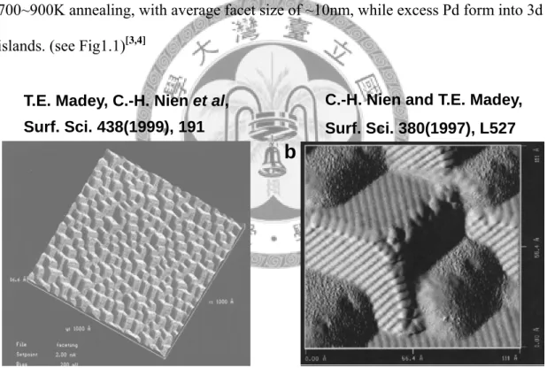
Faceting is pretty common in crystals of ionic or covalent compounds, and rarely seen on metallic surfaces, since metallic bonds are in general isotropic. Yet formation of pyramidal facets occurs when W(111) or Mo(111) surfaces are covered by Pd, Pt, Au, Ir, Rh, oxygen or sulfur. The deposited thin film increases the anisotropy in surface free energy, making the faceted surface become thermodynamically favored, but it is still limited kinetically, thus annealing is often required in the process[1]. For Pd/W(111) system, faceting occurs when Pd coverage is greater than 1.2 ML upon 700~900K annealing, with average facet size of ~10nm, while excess Pd form into 3d islands. (see Fig1.1)[3,4]
When tungsten surface is fully faceted, LEED spots corresponding to (111)
surface will vanish (see Fig 1.2 (a)), and spots corresponding to {112} surfaces appear, which form many characteristic clover-like triplets (Fig 1.2 (b)).
C.-H. Nien and T.E. Madey, Surf. Sci. 380(1997), L527 T.E. Madey, C.-H. Nien et al,
Surf. Sci. 438(1999), 191
Fig 1.1 (a) Pd(1.2ML) / W{112}, STM image, the surface is fully faceted (b) Pd(1.5ML) / W{112}, STM image, excess Pd forms 3d islands
a b
3
Research using field ion microscope (FIM)[5] shows that for a Pd coated tungsten tip, the tip surface near (111) orientation is also faceted and expose {112} facets. In addition, the apex of the pyramid is essentially one single Pd atom (Fig 1.3(a)).
Furthermore, if this atom is deliberately field evaporated from the surface, annealing alone can cause another Pd atom to diffuse and fit into this position (Fig 1.3(d)). Such self-repairing tendency due to thermodynamic stability of the faceted tip makes the search of faceting phenomenon a very effective screening method in identifying potential material systems that can easily reproduce well characterized single atom tips for applications in scanning tunneling microscopy (STM) or as the ultimate field emission sources of either electrons or ions.
Fig 1.2 LEED image at 112eV, 130K of (a) W(111), (b) Pd / W{112}
a b
4
Fig 1.3 FIM image from the apex of a pyramid. (a) A single atom is sitting on the
top. (b) The second layer consists of 3 atoms. (c) The third layer consists of 7 atoms, apparently 3 atoms are lost on the corners. (d) Regenerated pyramid, still a single atom is on the top. (e) The second layer still consists of 3 atoms. (f) There are 10 atoms this time... (g) There is one atom left after field evaporation of the third layer, probably being a W atom. (h) After field evaporation of several layers. It can be seen that the {112} surfaces are extending themselves.
These pictures are obtained from “The growth of pyramidal structure on Pd covered W tip and research on relative atomic processes”,
Lung-Chieh Cheng and Tsu-Yi Fu, National Taiwan Normal University Electronic Theses & Dissertations.
5
Chapter 2 Experiment
2.1 Experimental apparatus
Due to the sensitive nature of surface systems, reducing surface contamination is crucial and therefore all experiments are performed in ultra high vacuum (UHV) chamber with a base pressure < 2e-10 torr. To study the elemental composition and thermal stability of thin films, double pass cylindrical mirror analyzer (DPCMA) with coaxial electron gun and an SR810 lock-in amplifier are used to acquire Auger
spectrums, also an UTI 100C precision gas analyzer is used in TPD measurements.
The surface morphology (faceted / planar) and the crystalline structure are monitored via LEED pattern from an Omicron SPA-LEED system coupled with an Apogee Alta U6 CCD camera. Co and Ni thin films are deposited by Omicron UHV evaporator EFM-3; as for Pd it is carried out by a homemade evaporator with feedback control of emission current. The W(111) sample is mounted on a 4-axis manipulator with a liquid nitrogen (LN) dewar capable of cooling the sample down to 100K.
The W(111) sample is spot-wielded on two tantalum rods at each end, and the sample is heated by program controlled current. C-type thermocouple is spot-wielded onto the W(111) sample to measure the sample temperature. Knowing the heating current at any time, the heating current induced pickup voltage in the thermocouple is removed after calibrating the pickup resistance which is linear in sample temperature.
For experimental control and data acquisition, quick basic programs and Ni-DAQ provides piecewise linear temperature control and 16-bit resolution in A/D channels. The gated heating and signal integration for TPA measurement is controlled by homemade electronics with adjustable frequency and duty cycle.
6
2.2 Experimental method
For Auger spectrums, the modulation amplitude is set to 1eV to acquire good energy resolution, as for TPA measurements, it is set to 4eV for better S/N ratio.
Auger peaks and anti-peaks of W at 151.4 and 179eV, Pd at 317.8 and 330eV, Ni at 833.8 and 848eV, and Co at 762 and 775eV are used to track Auger intensity, and the frequency of gated heating is set to 30Hz to eliminate the 60Hz noise.
For TPD, 106Pd, 58Ni and 59Co are tracked to record spectrums, and an empty channel of mass 84 is also tracked to remove the background drift (which is in general very small, but the effect is not negligible in log scale).
For LEED, we use the phosphorescence screen and a CCD camera to take the LEED pattern instead of using the high resolution scanning mode, which SPA-LEED is designed for. This is due to the fact that the scanning mode requires 5 to 10 minutes to take one graph, and with the CCD camera it takes only 5 seconds. The trade off is, the LEED screen for SPA-LEED only reveals a relatively small solid angle, i.e., 14∘
in the Ewald sphere.
The amounts of adsorbates are measured in units of thermal desorption monolayer (TML), which is determined from the monolayer peak in the TPD spectrum. This is the amount of adsorbate that saturates the highest temperature desorption peak of that adsorbate.
7
Chapter 3 Results & Discussion
3.1 Ni / W(111) and Co / W(111) system
3.1.1 TPD spectrum and thickness calibration of Ni
To calibrate the deposition rate of Ni on W(111) surface, we fixed the e-beam heating current of the evaporator at 10mA while the high voltage is fixed at 1000V.
By varying the deposition time, we can get thin films of different thickness of Ni on the surface. Once the film is thermally desorbed, upon integrating the desorption rate with respect to time, total amount of the adsorbates can be found(on a relative scale).
Also, TPD spectrum provides information about the interactions between adsorbates and the surface, as desorption rate vs. temperature is correlated to the desorption activation energy. In general, the interaction between adsorbates and the surface is different from the adsorbate-adsorbate interaction. If the binding between the adsorbate and surface is stronger, one may expect that the adsorbate is capable of wetting the surface, and it is very likely to see two (or sometimes more) peaks in the TPD spectrum, which correspond to the multilayer desorption (at lower temperature) and the monolayer desorption (at higher temperature). Because the monolayer desorption is coming from the adsorbate-surface interaction, once the surface is fully covered, the amount of adsorbate will not affect the monolayer desorption curve. For example, in our previous work it is shown that Pd and Fe indeed exhibit this property on the W(111) surface. Otherwise if the adsorbate-adsorbate interaction is stronger, there can possibly be only one peak in the TPD spectrum. Again, Pd and Fe show this property on W(111) surface, after the surface is dosed with oxygen[2].
8
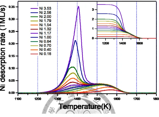
Since the multilayer peak and the monolayer peak are clearly distinguishable in the TPD for Ni on the W(111) surface, it shows that the Ni-W interaction is stronger than the Ni-Ni interaction, and we can define the amount of 1 TML to be that needed to saturate the high temperature peak.
Here we defined the amount of Ni under the blue curve to be 1 TML, as judging from the trend of the curves, it features only a very small shoulder at around 1380K and contains a complete monolayer peak.
Fig 3.1 TPD at a heating rate of 8K/s of various amount of Ni on W(111)
surface. Notice that the trailing edges of the monolayer peaks all converged for Ni above certain amount. Inset: Thickness of Ni (in units of TML) vs. Temperature (K)
9
After subtraction of the monolayer peak (Ni0.84) (Fig 3.2), it shows that for Ni 1.00~2.00 TML, the multilayer desorption rate reach the maximum value at
approximately the same temperature, 1370K. This is the characteristic feature for a first-order desorption, as modeled by the Polanyi-Wigner equation [6]:
dθ
dt ν θ exp Ea kT
Where θ is the amount of adsorbate on the surface, n is the order of desorption, ν is a constant (sometimes also a function in θ), and Ea is the desorption activation energy. In our case, the temperature is a linear function of time with a heating rate of 8K/s.
Observe that for n=1, if u(t) is a solution to the above equation, then u(t) multiplied by a constant is also a solution to the equation. Since this is a first order
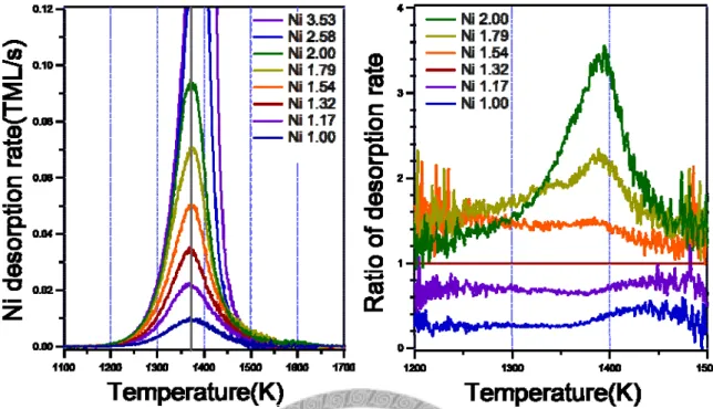
Fig 3.2 (a) TPD spectrum after monolayer peak subtraction, note that the multilayer peaks sit on the same temperature for Ni1.00~Ni2.00 (b) Ratio between desorption rates with respect to Ni 1.32. The ratio is
roughly constant throughout the range 1.00~1.54TML, and start to show some distortion from 1.79TML.
10
differential equation, c*u(t) then covers all the possible solutions. After dividing the desorption curves by Ni 1.32 (Fig. 3.2 (b)), one can see that for Ni1.00~Ni1.54, the ratio is essentially constant throughout the temperature ranging from 1250K to 1350K, and varied slightly after 1400K due to the fact that the monolayer desorption also occurs at such temperature thus distort the ratio. As for Ni > 1.79TML, the desorption curves start to diverge from the trend, and for Ni more than 2.5TML the peak position is even shifting to higher temperature. This means that the order of desorption is reducing from 1 to some lesser value when the total amount of Ni increases.
3.1.2 Electron attenuation length of Ni
Since the surface composition is tracked by Auger signal, it is crucial to find out the relation between Auger intensity and the thickness of Ni on the W(111) surface.
The electron attenuation length (EAL) is commonly understood to be a measure of the opacity of a solid for a given electron energy in AES and XPS. It is somehow different from the inelastic mean free path (IMFP) of electron, as the elastic-scattering of electrons in the solid may considerably influence their trajectories. The projection of a trajectory on a given direction could then have a significantly different length than the length actually traveled, and thus the EAL could differ from the IMFP[7].
For electrons emitted at an angle α to the normal from a solid surface, the Auger intensity from a source at a depth z below the surface follows the approximate
relation:
I I exp z
λcos α
Where λ is the EAL, and in our case α = 42.3∘for DPCMA.
11
From the AES of various thickness of Ni on W(111), Auger peak to peak value at different energy can be fitted to obtain the EAL of Ni at several energies (Fig 3.3):
Electron Energy(eV) 170 708 773 845
Experimental EAL (TML) 2.87 8.44 9.29 10.78
Calculated EAL(Å) [8] 3.44 10.19 10.96 11.82
Å / TML 1.20 1.21 1.18 1.10
Comparing the experimental and calculated EAL[8], we conclude that if the low temperature deposited film is homogeneous and flat, than 1TML should be equal to a thickness of 1.17Å, which is too small if TML≡PML. There can be two possibilities:
(1)1TML is equal to 1ML for Ni on W(111), or (2)the low temperature growth of Ni on W(111) is not epitaxial. At present, there is still no solid evidence to tell what the truth is, yet the EAL measured in unit of TML is self-consistent in our experiments.
Auger Sig.(arb. unit)
880 840 800 760 720 680
Electron Energy(eV)
Auger Sig.(arb. unit)
190 180 170 160 150
Electron Energy(eV)
Auger P-P amplitude(arb. unit)
121110987654321Ni amount(TML)
Ni 845eV Ni 773eV Ni 708eV W 170eV
Fig 3.3 (a) AES of Ni, (b) W of various thickness of Ni on W(111)
(c) Peak-to-peak Auger intensity vs. amount of Ni. Energy value shown in the annotation is the mean value of the peaks.
12
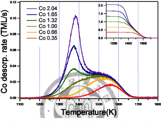
3.1.3 TPD spectrum and thickness calibration of Co
The desorption of Co is very similar to Ni, with a multilayer peak and converging monolayer peak. Not only the characteristic shape but also the temperature of desorption are almost the same in both cases, indicating that the binding strength of Ni-W and Co-W are very close to each other.
Both the deposition rate of Ni and Co is set to be 1TML / 90s in this experiment, which is appropriate for the thin film growth required in our study.
Fig 3.4 TPD at a heating rate of 8K/s of various amount of Co on W(111) surface. The desorption curves are similar to Ni, but with higher monolayer peak temperature and wider multilayer peak.
13
3.2 A quick survey on Co / Pd / W(111) system
Here we examined the thermal stability of Co thin film on Pd / W{112} faceted surface, and its effect on faceting phenomenon.
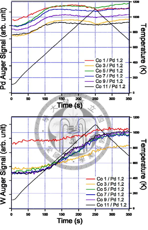
We prepared the W(111) sample by first flashing it to 2000K to remove surface residuals. 1.2TML of Pd is then deposited at 100K and annealed to 1000K to induce surface faceting. After annealing, 1TML of Co is deposited on the faceted surface initially while 2TML of Co is added successively onto the surface in later depositions.
After each deposition, temperature programmed Auger spectra is obtained while the sample is being annealed at a heating rate of 4K/s up to 1100K. LEED patterns are then taken at an incident energy of 792eV after the sample has been cooling down to 100K.
14
Fig 3.5 TPA signal of (a)Co, (b)Pd and (c)W, the sample is annealed (due to TPA) and added by 2TML of Co at each step .Apparently Co is forming 3D-islands on the surface upon annealing. Notice for Co more than 5TML, signal from W show similar trend.
15
PA shows that during heating, signal from Co drops as signal from Pd and W rises. This is most likely due to decreasing of the shielding effect of the Co film, which is most likely due to Co films agglomerate into 3-d islands. Notice that during cooling there is essentially no further change in TPA signal§, indicating whatever changes occurred during heating of the surface, they are irreversible and must be thermodynamically favored but kinetically limited when at low temperature.
There are many factors which can affect the thickness of a film, the most common ones are deposition and desorption. And in this case, since the desorption rate of both Co and Pd are too small to cause any observable effect , there must be something different happening on the surface.
§ Notice the Auger signal from W and Pd increased slightly during cooling. This effect is
actually temperature dependent as the signal of Pd is symmetrical in temperature from 700K to 1100K. This probably because the position of sample is altered by temperature, and the electron beam is out of focus at such high temperature.
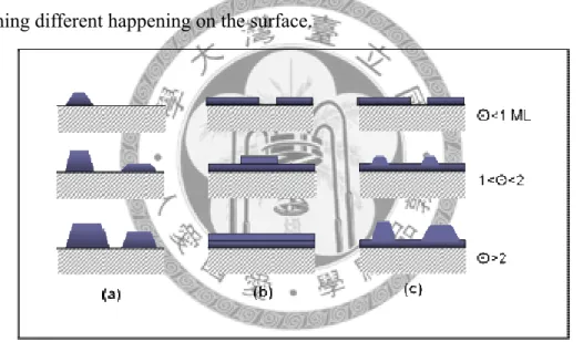
Fig 3.6 Cross-section views of the three primary modes of thin film growth including (a) Volmer-Weber (island formation), (b) Frank-van der Merwe (layer-by-layer), and (c) Stranski-Krastanov (layer-plus-island), for several different amounts of surface coverage[9].
16
As shown in Fig 3.6[9], the growth mode of a thin film can be roughly separated into three primary modes. When deposited at low temperature (such as 100K in our experiment), the mobility of adsorbates are quite small and the atoms should be frozen in at positions where they land on the surface. Since island formation is kinetically limited at this stage, the growth mode is very likely to be statistically uniform during deposition. As temperature rises, atoms gain enough energy to move around and the system may approach its thermodynamic stable state during annealing. In this case, since TPA trend show decrease in Co thickness, the thermodynamic stable state for Co thin film on Pd / W{112} faceted surface is probably VW type or SK type. 3D islands formation occurs when temperature rises, thus decreases the effective thickness of Co.
This phenomenon is also observed in our previous work on the Fe / Pd / W{112}
system[2] as well as the Ni / Pd / W{112} system, as we shall see later in section 3.3.
The ratios of Co and Pd Auger signals after and before annealing in these curves are very close (and also for ratios of W, if Co is more than 5TML), being around 0.73 and 1.23 respectively. This is probably because each time in this experiment, 2TML of Co is added onto the surface and formed into 3D islands repeatedly, with the ratio in Auger signal being the difference coming from layer by layer film growth and 3D islands. However, remember that from TPA data we can only see the trend of changes with their temperature dependence, and it is hard to tell such detailed morphology on the surface. A more appropriate instrument such as STM is required for any further studies in this topic.
LEED patterns after each TPA show that the surface still remains faceted to some extent throughout the whole experiment:
17
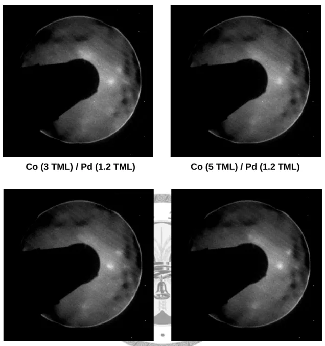
In Fig 3.7, it can be seen that LEED patterns are fuzzy after Co deposition and subsequent annealing, indicating the surface is very rough. Still LEED spots from the faceted surface can be observed without significant change when the amount of Co is varied. This is also consistent to our previous suggestion that Co is forming into 3D islands upon annealing, thus increases the overall surface roughness.
Fig 3.7 LEED patterns at 792eV of Co (xTML) / Pd (1.2 TML) / W{112}, after annealing. Bright background indicates increased surface roughness.
Co (3 TML) / Pd (1.2 TML)
Co (7 TML) / Pd (1.2 TML) Co (11 TML) / Pd (1.2 TML) Co (5 TML) / Pd (1.2 TML)
18
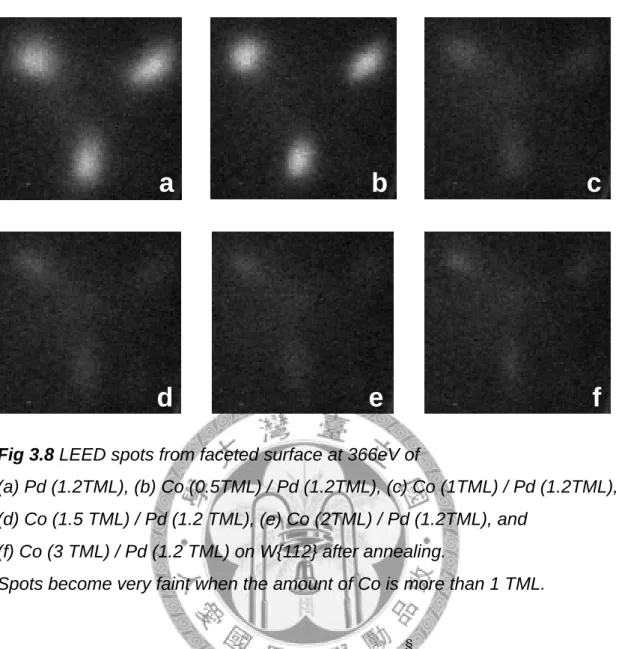
A more careful examination on this system (Fig 3.8)§ show that the LEED spots after annealing suddenly become very faint when the amount of Co is more than 1TML. This is not a good property for our goal as Co can possibly disturb the faceted surface and make it become rough. Also TPA shows significant changes when
temperature is higher than 300K, indicating poor thermal stability.
§ The electron energy is changed to 366eV in Fig 3.8 to reduce the brightness of
background from randomly scattered electrons and for proper intensity of LEED spots.
Fig 3.8 LEED spots from faceted surface at 366eV of
(a) Pd (1.2TML), (b) Co (0.5TML) / Pd (1.2TML), (c) Co (1TML) / Pd (1.2TML), (d) Co (1.5 TML) / Pd (1.2 TML), (e) Co (2TML) / Pd (1.2TML), and
(f) Co (3 TML) / Pd (1.2 TML) on W{112} after annealing.
Spots become very faint when the amount of Co is more than 1 TML.
a b c
d e f
19
Comparing the surface morphology of Co / Pd / W and Fe / Pd / W system (Fig 3.8 and Fig 3.9), Fe will cause the faceted surface to undergo defaceting transition and become planar, but Co will not, as we did not observe any LEED spots from W(111) surface up to 11TML in this experiment. This is actually an unexpected result since Fe and Co are next to each other on the periodic table, both of them are transition metal with ferromagnetic characteristic. However on second thought, because Co is more close to Pd, probably they share more similar property on the faceting phenomenon.
As far as we know, faceting does not occur for pure Co on W(111) at any coverage.
So the real reason for this difference is still a mystery.
Fig 3.9 LEED spots of (a)Fe 0.9TML, (b)Fe 1.7TML, (c)Fe 2.6TML, and
(d)Fe 3.4TML on Pd(4 TML) / W surface. The surface becomes planar when the amount of Fe is above a certain level. This graph is obtained from reference[2].
a b c d
20
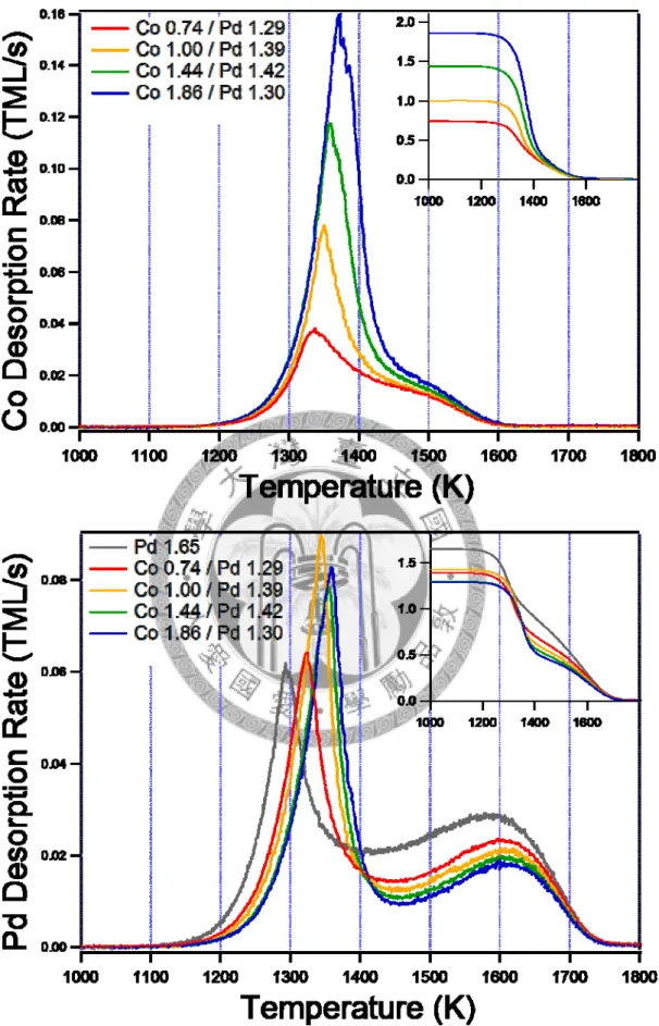
Fig 3.10 TPD of (a)Co and (b)Pd from Co / Pd / W surface. The insets are the amount of Co and Pd on the surface (TML) vs. Temperature (K). The annotation shows the initial amount of each adsorbate in TML.
21
TPD (Fig 3.10)§ on Co (x TML) / Pd (~1.3 TML) / W show that the desorption of both Co and Pd are very different from pure Co or Pd films. Multilayer desorption can be observed even when the amount of Co is less than 1TML, yet this is expected if there are 3D-islands forming on the surface. Co atoms in 3D-islands experience Co-Co interaction instead of Co-W interaction, thus they will be desorbed at lower temperature. Also the monolayer desorption of both Co and Pd are now depending on the total amount of Co. As we shall see later, this is an interesting phenomenon which is not observed previously in Fe / Pd / W system. It can be caused by phase separation or alloy formation of Pd and Co on the surface§§:
In either case, Pd can Co atoms right on the W substrate would cause the monolayer desorption, and their ratio would be depending on the relative abundance of these atoms. The difference between these two models is in the phase separation model, Pd-Pd or Co-Co interaction would be stronger than the Pd-Co interaction, and vice versa. On the phase diagram, Co and Pd bulk are fully miscible:
§ The amount of Pd is controlled by deposition time while using the same heating power
on the crucible, yet sometimes the deposition rate may vary during the experiment.
§§ Also an intermediate state of partial alloy formation at the boundary of Pd and Co can be
proposed, but the main point here is already made.
phase separation alloy formation
22
From the phase diagram[10]§, we suggest that alloy formation is very likely to occur in the 3D-islands or in the wetting layer. Also notice that the leading edge of multilayer desorption from Pd is shifting to higher temperature when the amount of Co increases. If phase separation is preferred on the surface, then the desorption from multilayer should be more like pure Pd, and their leading edge would overlap each other. Obviously it is not the case.
§ However, the ternary phase diagram of Co-Pd-W is nowhere to be found.
Fig 3.11 Co-Pd phase diagram shows Co and Pd are fully miscible in bulk below 1200 deg C. Graph is obtained from reference[10].
23
Comparing the desorption of Fe / Pd / W and Co / Pd / W system, it can be seen that there is no observable monolayer desorption for Fe. The trend of leading edges of Pd are similar in both cases, but different for Fe and Co respectively. The hints from monolayer desorption means that the first wetting layer is mainly composed of Pd in the Fe / Pd / W system, and both Co and Pd (which we suggested to be the alloy) in the Co / Pd / W system.
Currently we do not have any direct evidence (such as STM, SEM or LEEM) showing the dynamics on the surface. What we did was trying to recover the truth from all these circumstantial evidence. With all that hints provided from TPA, TPD and LEED, there is a good chance we can get the right idea about what’s really happening on the surface.
0.6 0.5 0.4 0.3 0.2 0.1
Desorption rate (PML/s)
1800 1750 1700 1650 1600 1550 1500 1450 1400 1350 1300 1250 1200 1150 1100
Temperature(K)
0.6 0.5 0.4 0.3 0.2 0.1 0.0
3.9 PML 4.2 PML 4.0 PML 3.9 PML Pd/W
0.81 PML 1.69 PML 2.23 PML 3.21 PML Fe/W
x10
x10
Pd desorption rate
Fe desorption rate Pd 4PML
Fe 0.8PML Fe 1.7PML Fe 2.2PML Fe 3.2PML
Fig 3.12 TPD of Pd and Fe from Fe / Pd / W surface. Notice that there is no
observable monolayer desorption from Fe. Also the leading edges from Pd are shifting to higher temperature, Fe to lower temperature as the amount of Fe increase. This graph is obtained from reference[2].
24
As a conclusion, it is verified in our experiment that the presence of Co on Pd / W{112} will change its thermodynamically preferred state, as 1 TML of Co would make the faceted surface become very rough after annealing. TPA show that observable changes occur at about 300K, indicating low thermal stability of Co film.
However, differing from the Fe / Pd / W system, there is no evidence showing that any amount of Co can cause defaceting of the surface. From the TPD data we suggest that Co and Pd are forming into alloy upon annealing, and this alloy is probably the cause of the entire phenomenon mentioned above.
For our goal, the Co / Pd / W system is not a very good choice in the aspect of thermal stability, however we did not completely rule out its possibility because the surface is still faceted after annealing (Fig 3.7, Fig3.8). STM study is required for further investigation on this topic.
25
3.3 The Ni / Pd / W(111) system
3.3.1 Thermal stability of Ni on Pd / W{112} faceted surface
In this experiment, we prepared samples with various amount of Ni on the Pd (1.5TML) / W{112} faceted surface.
W(111) sample is first flashed to 2000K to remove surface residuals, and then deposited with 1.5TML of Pd at 100K. After deposition, the sample is annealed to 1000K for 1 minute at a heating rate of 20K/s to induce faceting. At this stage, LEED patterns indicate the surface is fully faceted. Ni is then deposited at the rate of 1/90 TML/s onto the Pd / W{112} faceted surface which is at 100K. After sample deposition, TPA is first performed at a heating rate of 3K/s:
26
Fig 3.13 TPA signal of (a)Ni, (b)Pd and (c)W, 100K to 1000K at a heating rate of 3K/s starting from t=0s. Ni is deposited at t=-50s, and Auger signal is not tracked during deposition.
27
TPA shows that upon heating, Ni signal drops and the signal from underlying W rises in general, and this trend becomes more significant when the amount of Ni increases. In particular for Ni=3.90TML, it can be observed that the signal from Ni is dropping significantly, while the signal from Pd and W are rising from 360K to 600K (green region). Because Ni is not desorbed away at this temperature, this indicates the thin film of Ni is forming into 3D-islands on the surface, decreasing the effective thickness which can be seen in Auger. Except for very low Ni coverage (Ni 0.32TML), the signal from both Pd and W eventually converge to the same value after annealing, suggesting these surfaces are probably very similar.
A more careful inspection shows that there are some anomalies occurring around 600K, as the slope of Ni signal is changing there for high coverage of Ni (>2TML), the Pd signal is dropping for low coverage of Ni (<2TML), and the slope of W signal is also changing there for all the coverage of Ni. The anomalies can be caused by many things. As far as we know, there are several events on the surface which can be detected by TPA, with their effects being listed in the following:
(1) 3D-islands formation. Whatever thin film forms into 3D-islands will cause the effective thickness to decrease. As Auger is coverage-sensitive, signal from the film will also decrease while signal from underlying layers increase.
(2) Mixing of adsorbates or alloy formation. When two layers of different atoms are inter-diffusing into each other, the signal from the atoms of upper layer will decrease, signal from the lower layer will increase and the signal from other underlying layers in general should not be affected.
(3) When both (1) and (2) happened at the same time, the situation becomes quite complicated as the alloy may act very differently from the composing elements. With TPA data alone it will not be sufficient to decide all the dynamics on the surface.
28
Judging from the TPA, the Ni thin film is relatively stable under 360K (blue region), which shows no significant change at any coverage. At some higher
temperature (green region), alloy formation is probably happening because for Ni <
1TML, the signal of Pd is rising and the signal of Ni is falling, but W signal is not changing. As for Ni > 1 TML the amount of Ni is then sufficient to form into 3D-islands, which dominates the overall trend. At even higher temperature (yellow region, > 600K), the alloy itself is probably forming into 3D-islands, however from TPA data alone it is hard to tell the truth.
LEED patterns show that all these surfaces (up to Ni coverage of 4.1TML) remain faceted after annealing (see Fig 3.17 in page 33), which means once the
surface is faceted, it will remain faceted regardless of the amount of Ni deposited on it.
One interesting thing is, right after the deposition of Ni, the LEED spots become very faint. Only after annealing the LEED pattern become clear again. This indicates that even at 100K, the low temperature grown Ni on Pd / W{112} surface is not ordered.
Ni (2TML) / Pd (1.5TML) / W{112}
After Ni deposition
Ni (2TML) / Pd (1.5TML) / W{112}
1000K annealed
Fig 3.14 LEED pattern at 792eV of (a) faceted surface right after Ni deposition,
and (b) after further annealing at 1000K. The pattern is fuzzy right after deposition and become clear after annealing.
a b
29
.
Fig 3.15 TPD of Ni in (a)linear scale, inset: Ni amount on surface vs.Temp.
(b)Arrhenius plot of samples Ni (xTML) / Pd (~1.5TML) / W{112}.
The desorption of Ni is more close to a zero-order desorption.
30
After taking the LEED pattern, TPD is performed to determine the thickness of these films, also all adsorbates are removed in this process for the next sequence of sample preparation.
TPD data (Fig. 3.15 (a)) shows that for Ni, the desorption is now more likely to be a reaction of order zero as the leading edge of multilayer desorption overlap each other. Also the multilayer peak can be observed even when the amount of Ni is less than 1TML (Ni 0.65 / Pd 1.48, orange). The shape of monolayer peak is now
correlated to the total amount of Ni on the surface, which becomes higher and higher when the amount increases.
For a zero-order desorption, the desorption rate can be written as:
dθ
dt ν exp Ea kT
If we take the logarithm of desorption rate and plot against inverse temperature, an Arrhenius plot can be obtained which gives a straight line with slope equal
to –Ea/k, also the pre-exponential factor ν can be determined from its y-intercept.
In the Arrhenius plot (Fig. 3.15 (b)), it is more clear to see the desorption is indeed a zero-order reaction. The overlapping leading edges are essentially straight lines with sharp turning corners at the peak. The activation energy and
pre-exponential factor is found to be 4.36eV and 0.47TML/s here, respectively.
Comparing the desorption of Ni from Pd / W surface and the clean W(111) surface, the order of desorption is different in our experiment (however the desorption of Ni from W(111) may eventually change to zero-order when the amount of Ni is more than 4TML), and the dependence of monolayer peaks to the amount of Ni is also different (monolayer peaks will overlap each other if there is no Pd on the surface), which is very similar to the Co / Pd / W system.
31
Fig 3.16 TPD of Pd in (a)linear scale, inset: Pd amount on surface vs.Temp.
(b)Arrhenius plot of samples Ni (xTML) / Pd (~1.5TML) / W{112}.
32
Just as the desorption of Ni is affected by the presence of Pd on the surface, TPD data of Pd (Fig. 3.16) show that the desorption of Pd is also affected by Ni on the surface. As the amount of Ni increases, the multilayer desorption peak shifts to higher temperature, while the monolayer peak becomes lower and lower. The Arrhenius plot shows that despite of the temperature shifting of leading edges, the slopes are
essentially the same so as the activation energy. The activation energy is found to be 3.68eV here.
Combining the TPD data of Ni and Pd, the monolayer peaks seem to compensate each other: as one rises, another fall. This makes sense as the adsorption site on the surface is limited and kept constant, so should the total amount of adsorbate
interacting with the surface. However in our experiment the absolute amount of adsorbates are never known, and the unit TML obtained from experiment is also ambiguous in definition. These factors decrease the reliability of further analysis such as summing the TPD curves of different adsorbates.
33
Fig 3.17 LEED pattern @ 792eV of Ni (xTML) / Pd (1.5TML) / W{112}
system, after annealing. All these surfaces keep faceted after depositing Ni and 1000K annealing
Ni 0.32TML / Pd 1.34TML Ni 0.65TML / Pd 1.48TML
Ni 1.00TML / Pd 1.48TML
Ni 2.89TML / Pd 1.52TML
Ni 2.04TML / Pd 1.50TML
Ni 4.10TML / Pd 1.58TML
34
3.3.2 Ni and the faceting phenomenon of Pd / W(111)
We wish to know the effect of Ni on the faceting phenomenon, which is crucial as the faceting / defaceting transition can be disturbed by adsorbates other than Pd on the surface. For example, Fe on the Pd / W{112} faceted surface will form into 3D-islands upon annealing. These 3D-islands somehow suck the nearby Pd into its bulk, forming alloy with a ratio of Fe:Pd = 2:3 and decreasing the effective thickness of Pd, eventually causes the surface to defacet[2]. As mentioned in the previous section, Ni in the other hand will not cause a previously faceted surface to undergo defaceting.
Yet because Ni and Pd are intermiscible (Fig. 3.18)[11], it is very likely for Ni and Pd to form alloy on the surface and alter the faceting phenomenon, just as the Co / Pd / W system.
Fig 3.18 Ni-Pd binary Phase diagram. Ni and Pd are fully miscible.
Graph is obtained from Thermal Processing Technology Center, http://tptc.iit.edu/Center/research/PhaseDiagram/Content/result/
Al-Ni-Pd%20system/Ni-Pd.gif
35
Fig 3.19 TPA of Ni (1.0TML) / Pd (xTML) / W system with heating rate 3K/s, up to 1100K. Significant change is only observable when Pd is more than 1TML.
36
Here we prepared sample with various amount of Pd, and keep the amount of Ni constant as 1 TML. The same process as in previous section is preformed during sample preparation, including the annealing of sample after Pd deposition, except for the amount of Pd and Ni.
As TPA data shown in Fig 3.19, while changing the amount of Pd from 0.22TML to 0.82TML, not much change can be observed in the trend as the amount of both Ni and Pd is very small. But when the amount of Pd is more than 1.2TML, the surface would be faceted before the deposition of Ni (as the sample is annealed after Pd deposition), and the TPA signal would show similar trend to the Ni1.00 / Pd1.48 (yellow) line in Fig. 3.13.
From the TPA data, one may probably expect that the presence of Ni actually have no effect on the faceting phenomenon of Pd / W(111), because there are no observable changes when Pd is less than 1.2TML, just as a normal Pd / W(111) surface would be. But keep in mind that from Auger signal alone, it is not sufficient to determine all the dynamics on the surface. More specifically, if the Auger signal did show some changes, then it is certain there must be something happening on the surface, but it is insensitive to the surface structure or detailed morphology. That’s why we need LEED patterns and TPD data to get more information about what’s really going on.
In this case, the LEED pattern taken after TPA somehow show some interesting aspect about the Ni / Pd / W(111) system:
37
Fig 3.20 LEED pattern @792eV of Ni(1TML) / Pd(xTML) / W(111) system.
The faceting phenomenon occurs even when Pd is much less than 1TML, just because the presence of Ni on the surface.
Ni 1.0TML / Pd 0TML Ni 1.0TML / Pd 0.22TML
Ni 1.0TML / Pd 0.45TML
Ni 1.0TML / Pd 1.20TML
Ni 1.0TML / Pd 0.82TML
Ni 1.1TML / Pd 1.65TML
38
As one can readily see in Fig 3.20§, there are indeed something different happened which TPA did not tell us.
As mentioned before, the faceting phenomenon occur only when the amount of Pd is more than 1.2TML in Pd / W(111) system upon annealing. But when Ni is also on the surface, the amount of Pd required to induce faceting can be reduced.
Comparing the LEED pattern of Ni 1TML/ Pd 0.22TML and Ni 1TML / Pd0.45TML show that the intensity of (00) spot from W(111) becomes weaker, and the LEED spots corresponding to W{112} surfaces also show up. This is because at this stage the surface is only partially faceted: at some region tungsten undergo faceting transition, in other region it does not. This phenomenon is also observed in the original Pd / W system: When W(111) surface is covered by certain amount of Pd (~1.1TML), both (00) spot and W{112} spots can be observed in the LEED pattern after annealing.
Although the kinetics of the faceting phenomenon on W(111) is still not clear, it is known that Rh, Ir, Pd and Pt are capable of inducing the reconstruction of tungsten surface. Since Ni is in the same column as Pd and Pt, one may think it will probably act similarly in the process. However there is no evidence for pure Ni film induced faceting has been observed for any coverage or annealing temperature. It is then very likely to be the Ni-Pd alloy which is inducing faceting.
§ The bright region on the upper left side of the graphs shown here is due to the light from
RGA filament. Although a picture of background light is always taken and subtracted, sometimes there can still be some residual light that cannot be removed.
39
Fig 3.21 TPD of (a)Ni, (b)Pd of Ni (1.0TML) / Pd (xTML) / W(111) system in
linear scale. Notice how the desorption peaks of Ni is altered by Pd on the surface. The monolayer peaks from both elements seem to converge for Pd >1.20
40
TPD on this system (Fig 3.21) show that the desorption of Ni is greatly influenced by Pd on the surface. The monolayer peak is falling and the multilayer peak is rising as Pd become more and more on the surface, which makes sense as discussed in previous section, which the adsorption site on tungsten surface is limited.
The leading edge of multilayer desorption is shifting to higher temperature in the trend, similar to the trend observed from the desorption of Pd in previous section.
The desorption of Pd is also altered by Ni as the monolayer peaks are lowered comparing to pure Pd, and it seem to converge when more than 0.82TML. Apparently this are some connection between TPD trend and the surface morphology, as LEED shows these surfaces are fully faceted when Ni > 0.82TML. Also notice that the order of multilayer desorption is somewhere between 0 and 1 (more close to 1), which is different from pure Pd on W(111) (order 0).
It seems that the composition of first layer is fixed when Pd is more than a certain amount, as both monolayer peaks of Ni and Pd start to overlap for Pd >1TML.
This suggests that certain ratio in Ni and Pd is preferred on the tungsten surface, which also ruled out the possibility of simple phase separation. But again from TPD alone we do not know the absolute amount of both elements, and this fixed ratio is merely an indicator.
Combining all the information from TPD of this Ni / Pd / W(111) system, we suggest that Ni and Pd are forming into alloy on the surface, fist because the order of desorption for multilayer peaks are altered significantly for both Ni and Pd, and also the composition in the first layer contains both elements with some preferred ratio.
This is also very likely to happen since Ni and Pd are intermiscible. This alloy is probably the reason why Ni 1.0TML / Pd 0.45TML / W(111) surface become faceted after annealing, and a detailed analysis on the faceting phenomenon is carried out, in the next section.
41
3.3.3 The planar / faceted transition of Ni / Pd / W(111) system
Since the presence of Ni can virtually “help” the faceting of Pd / W(111) surface, here we wish to know the actual boundary of the planar/faceted transition.
In this experiment, first we prepared sample with various amount of Ni deposited on the surface, from 0TML to 1.0TML. Then 0.1TML of Pd is added onto the
surface and annealed until the LEED spots from W(111) is no longer observable or the intensity is comparable to background. After that, TPD is performed to check the amount of Pd and Ni.
LEED patterns are taken at 680eV here, just for decent (00) spot intensity. As shown in Fig 3.22, LEEDIV indicates the Bragg condition is at 711eV. At such energy the spot intensity from W(111) surface will reach its maximum, but also the spots from {112} surface is at the same position as the (111) spots. So we choose an energy which LEED spots from {112} surface is still distinguishable, but not too far away from the peak position.
(00) intensi ty (arb. unit)
1000 900
800 700
600 500
400 300
200
Electron Energy (eV)
Fig 3.22 LEEDIV of W(111) surface. Bragg condition occurs at the peak of electron energy=711eV.
42
Fig 3.23 The planar/faceted phase diagram of Ni / Pd / W(111) system, color annotation: green(planar), blue(faceted), purple(intermediate state), yellow(unknown). Spot intensity is re-stretched to log scale.
43
From Fig 3.23, it can be seen that the amount of Pd required to start the faceting phenomenon is greatly reduced by Ni. Especially for Pd (0.5TML) / Ni (0.8TML) / W, the surface is already partially faceted with such low Pd coverage.
Notice that the planar / intermediate state boundary is not a straight line on the diagram. As pure Ni cannot induce faceting, at least certain amount of Pd is required.
Also a significant change can be observed around Ni~0.3TML, indicating something different is happening at such coverage.
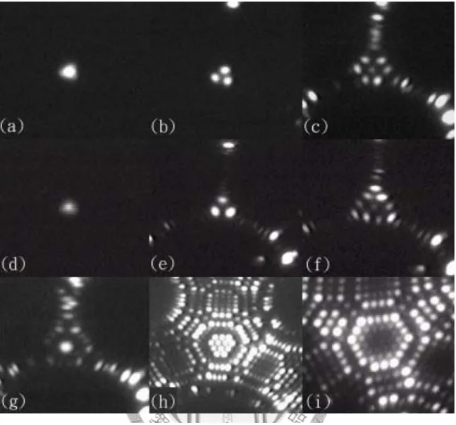
The LEED patterns in the yellow region on the diagram (bottom right corner) show 3 spots surrounding the (00) spot, however not only their shape are different from the spots coming from {112} surface (compare Ni 1.0 / Pd 0.5 and Ni 1.0 / Pd 0.4), but their position are also different at various electron energy (Fig 3.24). These spots is more likely to be coming from a superstructure instead of the {112} surface, with characteristics of 6x6 reconstruction. Yet when the amount of Pd is enough to induce the faceting phenomenon, no satellite spot is observed other than {112}. This effect is only observed when the amount of Ni is about (and probably more than) 1TML. The actual mechanism of such reconstruction is still unknown.
For more detailed analysis on Fig 3.23, we can integrate the spot intensity of the (00) spot and the faceted spot on each LEED pattern, then plot them against the amount of Pd (Fig 3.25):
44
Fig 3.24 LEED pattern of (a,c) Ni 1.0 / Pd 0.2 / W and (b,d) Ni 1.0 / Pd 0.8 / W
at various electron energy. Notice the position of the spots surrounding the (00) spot are different.
670eV 680eV 690eV
700eV 792eV 930eV
a
b
c
d
45
From Fig 3.25, it is clearer how the planar/faceted transition boundary is shifted toward lower Pd amount. First there is without any doubt that at final state the intensity of the LEED spots from the faceted surface are higher than the (00) spot from original (111) surface for every sample. Also the trend of Ni 0.8(purple) and Ni 1.0(black) are similar, showing that the real benefit from Ni on the faceting phenomenon is in the range Ni<1TML.
Fig 3.25 The integrated spot intensity of (00) spot and spots from the {112}
faceted surface @ 680eV vs. the amount of Pd. It is clearer that the planar/faceted transition boundary is shifted toward lower Pd amount.
46
Fig 3.26 TPD from the top state of each column in Fig 3.23, which LEED spots from W(111) is not observable. The desorption of Pd show very similar shape.
47
TPD from the final state in each column of Fig 3.23 (Fig 3.26) show that the desorption curves of both Pd and Ni have very similar shape in this series, especially for the samples with Ni 0.2TML~Ni 0.6TML. This may be the characteristic when the amount of Pd is just enough to make the surface fully faceted, as one can imagine that it have to be completely covered by Pd or the Ni-Pd alloy, thus the desorption will show a monolayer peak with some multilayer desorption, but not too much. For samples with Ni>0.6TML, one can tell from Fig 3.25 (orange and red curves) that the amount of Pd is probably a little bit too much, since the intensity of LEED spots show no significant change at the last few steps. This is probably the reason why the
multilayer desorption peaks are higher than others on these samples in Fig 3.26.
As a conclusion, the Ni / Pd / W system is better than the Fe / Pd / W and the Co / Pd / W system in both thermal stability and its effect on faceting phenomenon. A detailed investigation is carried out for Ni / Pd / W system and the boundary of
faceted / planar transition on the surface is found. The combination which is closest to our goal is the Ni / Pd / W near this boundary. The second best combination is
probably the Ni (x TML) / Pd / W faceted surface, which is stable under ~400K. The third best is the Fe / Pd / W system, although the thermodynamic stable state of the surface may become planar if the amount of Fe is too high. However, measurement of magnetic property is not carried out in this experiment, and we are now planning to add a MOKE system to our vacuum chamber.
48
Chapter 4 Summary
The Co / Pd / W(111) system is similar to the Ni / Pd / W(111) system in the aspect of adsorption behavior. From the binary phase diagram, Co-Pd and Ni-Pd are fully miscible. TPD data indicates strong interactions between Co-Pd and Ni-Pd on the surface, as the desorption curves of the Co/Pd/W and Ni/Pd/W trimetallic systems are very different from the bimetallic ones. This suggests Co and Ni tend to form alloy with Pd on the surface. LEED show that the presence of Co will make the spots from the faceted surfaces very faint, while no spots from planar (111) surface can be observed. As for Ni, we found that Ni can reduce the required amount of Pd to induce the faceting of W(111) surface. From the aspect of thermal stability, TPA show that all thick films (>1TML) of Ni or Pd on the faceted surface tend to form 3D-islands upon annealing, the thermal stability of Ni films are around 360K, while Co films have rather poor stability (<300K). This indicates such thick films are unlikely to be candidates for forming magnetic single atom tips. Still from this experiment we have found that thin films of Ni / Pd / W(111) system, which near the faceted/planar phase boundary, have pretty well thermal stability. These are the systems in which there is still hope and warrants a MOKE measurement in the future.
49
Reference
1. Madey, Theodore E.; Guan, J.; Nien, C.-H.; Dong, C.-Z.; Tao, H.-S.; Campbell, R. A., Surface Review and Letters, Vol. 3, Issue 02(1996), 1315-1328.
2. Faceting of W(111) induced by Fe, Pd thin films and adsorption of hydrogen and CO on these surfaces, Chang-Han and Huang and K. J. Song, NTU Institutional Repository, http://ntur.lib.ntu.edu.tw/handle/246246/181081
3. T.E. Madey, C.-H. Nien et al, Surface Science, 438(1999), 191.
4. C.-H. Nien and T.E. Madey, Surface Science, 380(1997), L527.
5. The growth of pyramidal structure on Pd covered W tip and research on relative atomic processes, Lung-Chieh Cheng and Tsu-Yi Fu, National Taiwan Normal University Electronic Theses & Dissertations,
http://etds.lib.ntnu.edu.tw/cgi-bin/gs/ntnugsweb.cgi?o=dntnucdr&i=sid=%
2290NTNU0198012%22.&searchmode=basic
6. Thermal desorption from metal surfaces: A review, David A. King, Surface Science, Vol. 47, Issue 1(1975), 384-402.
7. The electron attenuation length revisited, A. Jablonski and C. J. Powell, Surface Science Reports, Vol. 47, Issues 2-3(2002), 33-91.
8. Values are calculated by NIST Standard Reference Database 82, NIST Electron Effective-Attenuation-Length Database.
9. Wikipedia: Stranski-Krastanov growth,
http://en.wikipedia.org/wiki/Stranski-Krastanov_growth
50
10. The Co-Pd (Cobalt-Palladium) System, K. Ishida and T. Nishizawa, Journal of Phase Equilibria, Vol. 12, No. 1(1991), 84.
11. Thermal Processing Technology Center,
http://tptc.iit.edu/Center/research/PhaseDiagram/Content/result/Al-Ni-Pd
%20system/Ni-Pd.gif
51
Appendix
Fig A.1 TPA of Ni (xTML) / W system. Ni tend to form 3D-islands upon annealing, and the thermal stability decreases when the amount of Ni increases.
52
Fig A.2 TPA of Co (xTML) / W system. Co tend to form 3D-islands upon annealing, and the thermal stability seems to be poor for pure Co film on the surface.
53
792eV F-P
TPD from p-t to t-f
1.4 1.3 1.2 1.1 1.0 0.9 0.8 0.7 0.6 0.5 0.4 0.3
0.2
0
0.10.2 0.3 0.4
0.50.6
0.70.8
0.91.0 Pd
Ni
Faceted
Planar
LEED 00, linear scale
@ 792eV
Fig A.3 The planar/faceted phase diagram of Ni / Pd / W(111) system, with electron energy at 792eV. The intensity of LEED spots from {112}
surface is stronger at this energy.
54
Fig A.4 Comparison of TPD data of Ni / Pd / W system, near the planar/faceted phase transition. Green curves correspond to the amount of Pd
required to start the faceting phenomenon, and blue curves correspond to the amount of Pd required to make the surface completely faceted.
The planar / faceted phase transition of the surface occur only when the desorption of Pd start to show the multilayer part.
55
Fig A.5 Comparison of LEED patterns between the superstructure phase, the Ni / Pd / W faceted phase and Pd / W faceted phase at several energy.
The spot position of Ni / Pd / W faceted surface is slightly different from the spot position of Pd / W faceted surface.
56
Fig A.6 LEED patterns of Ni (1.0TML) / Pd (0.5TML) / W(111) surface after
annealing to various temperature. The faceting phenomenon occur at around 750K, this change of the surface morphology was not
observed in the TPA signal in Fig 3.19