Studies of band alignment and two-dimensional electron gas in InGaPN / GaAs heterostructures
J. S. Hwang,a兲K. I. Lin, H. C. Lin, S. H. Hsu,b兲 K. C. Chen, and Y. T. Lu Department of Physics, National Cheng Kung University, Tainan 701, Taiwan Y. G. Hong and C. W. Tu
Department of Electrical and Computer Engineering, University of California, San Diego, La Jolla, California 92093-0407
共Received 18 October 2004; accepted 30 November 2004; published online 1 February 2005兲 Room-temperature photoreflectance 共PR兲 and photoluminescence 共PL兲 spectra are measured for a series of In0.54Ga0.46P1−yNy/ GaAs heterostructures grown on GaAs共100兲 substrate. Redshifts of the PR and PL peaks indicate that the band gap of In0.54Ga0.46P1−yNyis dramatically reduced as nitrogen is incorporated. The emergence of additional peaks in PR spectra as nitrogen is incorporated indicates that the band alignment switches from type I to type II, due to the lowering of the conduction band, thus forming a two-dimensional electron gas 共2DEG兲 in the interface region between In0.54Ga0.46P1−yNy and GaAs. The band gap energy and transition energies between the confined levels in the 2DEG are determined for samples with various nitrogen concentrations y. The number of confined levels in the 2DEG is found to increase with y; the composition-dependent bowing parameter is determined. © 2005 American Institute of Physics.关DOI: 10.1063/1.1855406兴
Lattice-matched In0.49Ga0.51P grown on a GaAs substrate has recently attracted considerable attention; it has been widely used in optoelectronic and electronic devices, such as semiconductor lasers,1 heterojunction bipolar transistors,2 and high efficiency tandem solar cells. A small amount of nitrogen incorporation is known to reduce dramatically the band gap energy in InGaAs; the reduction results mostly from the lowering of the conduction band.3 The nitrogen incorporated into InGaP has recently been reported to have a similar effect.4–6 However, few relevant research reports have been published. Additionally, most studies have em- ployed photoluminescence共PL兲 spectra at low temperature;
therefore, most of the electro-optical properties examined have been limited to low temperature. Detailed studies of the electro-optical characteristics at room temperature and high temperature are interesting, necessary, and important.
This letter describes the feasibility of using room- temperature photoreflectance spectroscopy共PR兲 to elucidate the electro-optical properties of a series of In0.54Ga0.46P1−yNy/ GaAs heterostructures. The PR spectra enable the band gap energy, band alignment, built-in electric field, and transition energies between the confined levels of the two-dimensional electron gas 共2DEG兲 to be accurately determined at various contents of incorporated nitrogen.
Room-temperature PL spectra are also measured in this study to verify some results from PR studies. Experimental results reveal that, as y艌0.005, the band offset of the conduction band of In0.54Ga0.46P1−yNyfalls dramatically so that the band alignment switches from type I to type II, and a 2DEG forms at the interface in the heterostructures. The band offset and thus the number of transition energies in 2DEG increases with the content of the incorporated nitrogen.
In0.54Ga0.46P1−yNy/ GaAs heterostructures are grown on 共1 0 0兲 GaAs semi-insulating substrate by gas source mo- lecular beam epitaxy. The growth sequence entails a 0.5-
m-thick In0.54Ga0.46P1−yNy 共y=0–2%兲 undoped layer grown on a 0.2m thickness of a GaAs buffer layer which is first grown on the GaAs substrate. The growth temperature at the substrate ranges between 340 and 480 ° C with a ni- trogen plasma ignited. No samples are thermal annealed. The mole fractions and lattice mismatch between In0.54Ga0.46P1−yNy and GaAs were determined by double- crystal x-ray diffractometry. All samples possess compres- sive strain on the GaAs buffer layer. The strain decreases as the nitrogen content increases. Table I lists the lattice mis- matches of samples with various nitrogen concentrations.
PL was measured at room temperature with the 532 nm line of a solid-state laser as the excitation source. A Si pho- todetector was used to detect the signal through a lock-in amplifier at the exit of a quarter meter monochromator. The standard arrangement of the PR apparatus was used. He–Cd or He–Ne laser served as the pumping beam. The detection system comprises a Si photodetector and a lock-in amplifier.
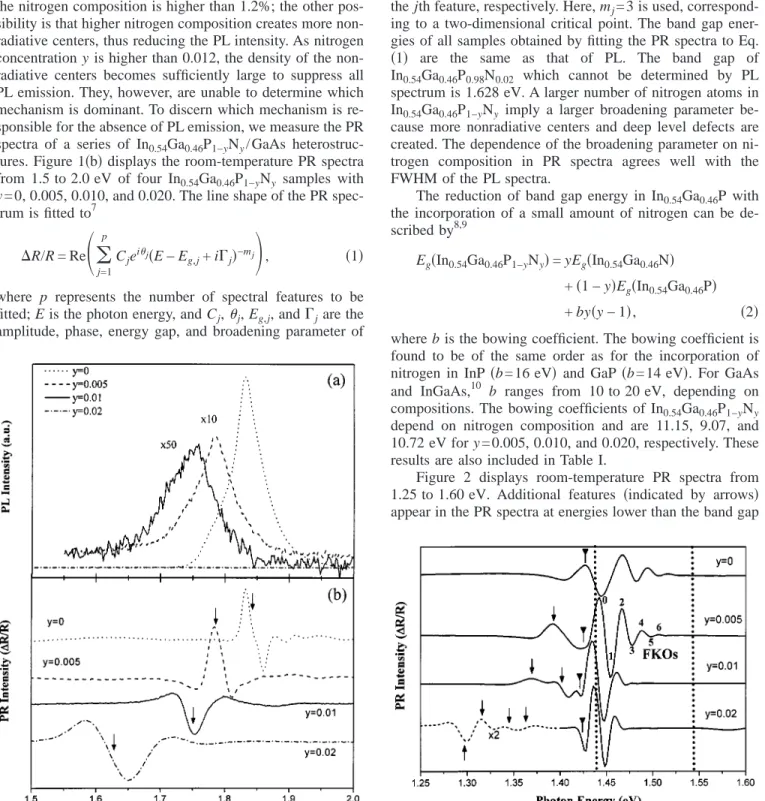
Figure 1共a兲 depicts the room-temperature PL spectra of three In0.54Ga0.46P1−yNysamples with y = 0, 0.005, and 0.010, respectively. No PL signal is observed in the sample with y
= 0.020. As the nitrogen concentration increases, the PL in- tensity decreases rapidly. Additionally, the peak position shows a redshift, apparently indicating that the band gap en- ergy of In0.54Ga0.46P1−yNy reduces markedly; and the full width at half maximum共FWHM兲 of the peak broadens con- siderably as well. The band gap energies which correspond to the peak positions are 1.832, 1.786, and 1.750 eV for samples with y = 0, 0.005, and 0.010, respectively. Hong et al.4 have found no GaAs QW PL emission from In0.54Ga0.46P1−yNy/ GaAs/ In0.54Ga0.46P1−yNy multiple quan- tum well when y is equal to or larger than 0.012. Two pos- sibilities are suggested. One is that high nitrogen composi- tion lowers the level of the conduction band so much that the energy band alignment switches from type I to type II when
a兲Author to whom correspondence should be addressed; electronic mail:
b兲Also with: Institute of Microelectronics, Department of Electrical Engi- neering, National Cheng Kung University.
APPLIED PHYSICS LETTERS 86, 061103共2005兲
0003-6951/2005/86共6兲/061103/3/$22.50 86, 061103-1 © 2005 American Institute of Physics Downloaded 02 Jul 2009 to 140.116.208.56. Redistribution subject to AIP license or copyright; see http://apl.aip.org/apl/copyright.jsp
the nitrogen composition is higher than 1.2%; the other pos- sibility is that higher nitrogen composition creates more non- radiative centers, thus reducing the PL intensity. As nitrogen concentration y is higher than 0.012, the density of the non- radiative centers becomes sufficiently large to suppress all PL emission. They, however, are unable to determine which mechanism is dominant. To discern which mechanism is re- sponsible for the absence of PL emission, we measure the PR spectra of a series of In0.54Ga0.46P1−yNy/ GaAs heterostruc- tures. Figure 1共b兲 displays the room-temperature PR spectra from 1.5 to 2.0 eV of four In0.54Ga0.46P1−yNy samples with y = 0, 0.005, 0.010, and 0.020. The line shape of the PR spec- trum is fitted to7
⌬R/R = Re
冉
兺j=1p Cjeij共E − Eg,j+ i⌫j兲−mj冊
, 共1兲where p represents the number of spectral features to be fitted; E is the photon energy, and Cj,j, Eg,j, and⌫jare the amplitude, phase, energy gap, and broadening parameter of
the jth feature, respectively. Here, mj= 3 is used, correspond- ing to a two-dimensional critical point. The band gap ener- gies of all samples obtained by fitting the PR spectra to Eq.
共1兲 are the same as that of PL. The band gap of In0.54Ga0.46P0.98N0.02 which cannot be determined by PL spectrum is 1.628 eV. A larger number of nitrogen atoms in In0.54Ga0.46P1−yNy imply a larger broadening parameter be- cause more nonradiative centers and deep level defects are created. The dependence of the broadening parameter on ni- trogen composition in PR spectra agrees well with the FWHM of the PL spectra.
The reduction of band gap energy in In0.54Ga0.46P with the incorporation of a small amount of nitrogen can be de- scribed by8,9
Eg共In0.54Ga0.46P1−yNy兲 = yEg共In0.54Ga0.46N兲 +共1 − y兲Eg共In0.54Ga0.46P兲
+ by共y − 1兲, 共2兲
where b is the bowing coefficient. The bowing coefficient is found to be of the same order as for the incorporation of nitrogen in InP共b=16 eV兲 and GaP 共b=14 eV兲. For GaAs and InGaAs,10 b ranges from 10 to 20 eV, depending on compositions. The bowing coefficients of In0.54Ga0.46P1−yNy depend on nitrogen composition and are 11.15, 9.07, and 10.72 eV for y = 0.005, 0.010, and 0.020, respectively. These results are also included in Table I.
Figure 2 displays room-temperature PR spectra from 1.25 to 1.60 eV. Additional features 共indicated by arrows兲 appear in the PR spectra at energies lower than the band gap
TABLE I. The sample composition, lattice mismatch, bowing parameter, energy of band gap, energy levels of 2DEG and the electric field at the interface between GaAs and In0.54Ga0.46P1−yNy.
y
Mismatch 共⌬d/d兲⬜
⫻10−3
Bowing parameter b共y兲 共eV兲
Egof InGaPN共eV兲 Egof GaAs 共eV兲
PR
Energy levels of 2DEG共eV兲 Electric field at the interface
共kV/cm兲
PR PL E1 E2 E3 E4
0 8.20 ¯ 1.843 1.832 1.427 ¯ ¯ ¯ ¯ 25.9
0.005 8.09 11.15 1.786 1.786 1.425 1.393 ¯ ¯ ¯ 17.8
0.010 7.12 9.07 1.751 1.750 1.421 1.369 1.402 ¯ ¯ 16.2
0.020 6.45 10.72 1.628 ¯ 1.424 1.297 1.316 1.345 1.363 14.1
FIG. 1. Room-temperature PL and PR spectra of In0.54Ga0.46P1−yNylayers on GaAs with various N content y. The arrows in共b兲 mark the fundamental gap of In0.54Ga0.46P1−yNy.
FIG. 2. Room-temperature PR spectra of In0.54Ga0.46P1−yNy/ GaAs samples pumped using He–Ne 633 nm laser. The arrows indicate the transition en- ergies of 2DEG while the symbol共䉲兲 points out the band gap energies of GaAs.
061103-2 Hwanget al. Appl. Phys. Lett. 86, 061103共2005兲
Downloaded 02 Jul 2009 to 140.116.208.56. Redistribution subject to AIP license or copyright; see http://apl.aip.org/apl/copyright.jsp
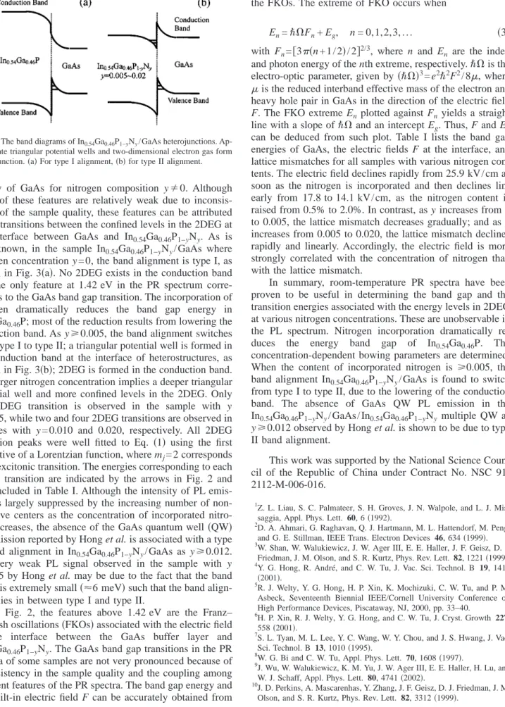
energy of GaAs for nitrogen composition y⫽0. Although some of these features are relatively weak due to inconsis- tency of the sample quality, these features can be attributed to the transitions between the confined levels in the 2DEG at the interface between GaAs and In0.54Ga0.46P1−yNy. As is well known, in the sample In0.54Ga0.46P1−yNy/ GaAs where nitrogen concentration y = 0, the band alignment is type I, as shown in Fig. 3共a兲. No 2DEG exists in the conduction band and the only feature at 1.42 eV in the PR spectrum corre- sponds to the GaAs band gap transition. The incorporation of nitrogen dramatically reduces the band gap energy in In0.54Ga0.46P; most of the reduction results from lowering the conduction band. As y艌0.005, the band alignment switches from type I to type II; a triangular potential well is formed in the conduction band at the interface of heterostructures, as shown in Fig. 3共b兲; 2DEG is formed in the conduction band.
The larger nitrogen concentration implies a deeper triangular potential well and more confined levels in the 2DEG. Only one 2DEG transition is observed in the sample with y
= 0.005, while two and four 2DEG transitions are observed in samples with y = 0.010 and 0.020, respectively. All 2DEG transition peaks were well fitted to Eq. 共1兲 using the first derivative of a Lorentzian function, where mj= 2 corresponds to an excitonic transition. The energies corresponding to each 2DEG transition are indicated by the arrows in Fig. 2 and also included in Table I. Although the intensity of PL emis- sion is largely suppressed by the increasing number of non- radiative centers as the concentration of incorporated nitro- gen increases, the absence of the GaAs quantum well共QW兲 PL emission reported by Hong et al. is associated with a type II band alignment in In0.54Ga0.46P1−yNy/ GaAs as y艌0.012.
The very weak PL signal observed in the sample with y
= 0.005 by Hong et al. may be due to the fact that the band offset is extremely small共⬇6 meV兲 such that the band align- ment lies in between type I and type II.
In Fig. 2, the features above 1.42 eV are the Franz–
Keldysh oscillations共FKOs兲 associated with the electric field at the interface between the GaAs buffer layer and In0.54Ga0.46P1−yNy. The GaAs band gap transitions in the PR spectra of some samples are not very pronounced because of inconsistency in the sample quality and the coupling among different features of the PR spectra. The band gap energy and the built-in electric field F can be accurately obtained from
the FKOs. The extreme of FKO occurs when
En=ប⍀Fn+ Eg, n = 0,1,2,3, . . . 共3兲 with Fn=关3共n+1/2兲/2兴2/3, where n and En are the index and photon energy of the nth extreme, respectively.ប⍀ is the electro-optic parameter, given by共ប⍀兲3= e2ប2F2/ 8, where
is the reduced interband effective mass of the electron and heavy hole pair in GaAs in the direction of the electric field F. The FKO extreme Enplotted against Fn yields a straight line with a slope ofប⍀ and an intercept Eg. Thus, F and Eg can be deduced from such plot. Table I lists the band gap energies of GaAs, the electric fields F at the interface, and lattice mismatches for all samples with various nitrogen con- tents. The electric field declines rapidly from 25.9 kV/ cm as soon as the nitrogen is incorporated and then declines lin- early from 17.8 to 14.1 kV/ cm, as the nitrogen content is raised from 0.5% to 2.0%. In contrast, as y increases from 0 to 0.005, the lattice mismatch decreases gradually; and as y increases from 0.005 to 0.020, the lattice mismatch declines rapidly and linearly. Accordingly, the electric field is more strongly correlated with the concentration of nitrogen than with the lattice mismatch.
In summary, room-temperature PR spectra have been proven to be useful in determining the band gap and the transition energies associated with the energy levels in 2DEG at various nitrogen concentrations. These are unobservable in the PL spectrum. Nitrogen incorporation dramatically re- duces the energy band gap of In0.54Ga0.46P. The concentration-dependent bowing parameters are determined.
When the content of incorporated nitrogen is 艌0.005, the band alignment In0.54Ga0.46P1−yNy/ GaAs is found to switch from type I to type II, due to the lowering of the conduction band. The absence of GaAs QW PL emission in the In0.54Ga0.46P1−yNy/ GaAs/ In0.54Ga0.46P1−yNy multiple QW as y艌0.012 observed by Hong et al. is shown to be due to type II band alignment.
This work was supported by the National Science Coun- cil of the Republic of China under Contract No. NSC 91- 2112-M-006-016.
1Z. L. Liau, S. C. Palmateer, S. H. Groves, J. N. Walpole, and L. J. Mis- saggia, Appl. Phys. Lett. 60, 6共1992兲.
2D. A. Ahmari, G. Raghavan, Q. J. Hartmann, M. L. Hattendorf, M. Peng, and G. E. Stillman, IEEE Trans. Electron Devices 46, 634共1999兲.
3W. Shan, W. Walukiewicz, J. W. Ager III, E. E. Haller, J. F. Geisz, D. J.
Friedman, J. M. Olson, and S. R. Kurtz, Phys. Rev. Lett. 82, 1221共1999兲.
4Y. G. Hong, R. André, and C. W. Tu, J. Vac. Sci. Technol. B 19, 1413 共2001兲.
5R. J. Welty, Y. G. Hong, H. P. Xin, K. Mochizuki, C. W. Tu, and P. M.
Asbeck, Seventeenth Biennial IEEE/Cornell University Conference on High Performance Devices, Piscataway, NJ, 2000, pp. 33–40.
6H. P. Xin, R. J. Welty, Y. G. Hong, and C. W. Tu, J. Cryst. Growth 227, 558共2001兲.
7S. L. Tyan, M. L. Lee, Y. C. Wang, W. Y. Chou, and J. S. Hwang, J. Vac.
Sci. Technol. B 13, 1010共1995兲.
8W. G. Bi and C. W. Tu, Appl. Phys. Lett. 70, 1608共1997兲.
9J. Wu, W. Walukiewicz, K. M. Yu, J. W. Ager III, E. E. Haller, H. Lu, and W. J. Schaff, Appl. Phys. Lett. 80, 4741共2002兲.
10J. D. Perkins, A. Mascarenhas, Y. Zhang, J. F. Geisz, D. J. Friedman, J. M.
Olson, and S. R. Kurtz, Phys. Rev. Lett. 82, 3312共1999兲.
FIG. 3. The band diagrams of In0.54Ga0.46P1−yNy/ GaAs heterojunctions. Ap- proximate triangular potential wells and two-dimensional electron gas form at the junction.共a兲 For type I alignment, 共b兲 for type II alignment.
061103-3 Hwanget al. Appl. Phys. Lett. 86, 061103共2005兲
Downloaded 02 Jul 2009 to 140.116.208.56. Redistribution subject to AIP license or copyright; see http://apl.aip.org/apl/copyright.jsp