Robustness of a Topologically
Protected Surface State in a
Sb
2
Te
2
Se Single Crystal
Chao-Kuei Lee
1,2, Cheng-Maw Cheng
2,3, Shih-Chang Weng
3, Wei-Chuan Chen
3,
Ku-Ding Tsuei
3, Shih-Hsun Yu
4, Mitch Ming-Chi Chou
4, Ching-Wen Chang
2, Li-Wei Tu
2,5,
Hung-Duen Yang
2, Chih-Wei Luo
6& Marin M. Gospodinov
7A topological insulator (TI) is a quantum material in a new class with attractive properties for physical and technological applications. Here we derive the electronic structure of highly crystalline Sb2Te2Se
single crystals studied with angle-resolved photoemission spectra. The result of band mapping reveals that the Sb2Te2Se compound behaves as a p-type semiconductor and has an isolated Dirac cone of a
topological surface state, which is highly favored for spintronic and thermoelectric devices because of the dissipation-less surface state and the decreased scattering from bulk bands. More importantly, the topological surface state and doping level in Sb2Te2Se are difficult to alter for a cleaved surface exposed
to air; the robustness of the topological surface state defined in our data indicates that this Sb2Te2Se
compound has a great potential for future atmospheric applications.
A topological insulator (TI) is a quantum material in a new class with attractive properties for physical and tech-nological applications because of its potential in spintronic devices1–6. Two-dimensional (2D) TI are typically
associated with gapless edge states; three-dimensional TI are associated with gapless surface states. The edge and surface states in these systems generally reveal a Dirac-cone-like dispersion; the spin degeneracy of Dirac fermions in these states of TI is removed and locked to the momentum, as these surface states of 3D TI exhibit a helical spin structure with the spin vectors parallel to the surface and perpendicular to momentum k. This unique topological phase offers a platform to realize diverse quantum phenomena, such as a topological magnetoelectric effect7, a Majorana fermion8, the quantum spin-Hall effect9 and spintronic applications10.
A key to develop applications in topological quantum computing7,11 and low- power spintronic devices10 is
that the dissipation-less surface states must be in the topological transport regime; specifically, the presence of an isolated Dirac cone is highly favoured because of the decreased scattering from bulk bands. Manipulating the position of the Dirac point in TI for future applications becomes a crucial problem. TI in the bismuth family – Bi2Se3, Bi2Te3 and Sb2Te3 – have a tetradymite structure, which consists of covalently bonded quintuple layers
(QL) with a weak interaction through a van der Waals force within QL12. Bi
2Se3 and Bi2Te3 have the chemistry of
a non-stoichiometric compound13,14; both compounds are invariably doped through the crystal defects, which
results in the transport properties being affected by bulk carriers. A single crystal of Bi2Se3 invariably exhibits a
n-type doping behaviour because of the Se vacancies or anti-site defects15,16. Regarding the Bi
2Te3 compound,
both n-type and p-type behaviour can be achieved on varying the initial composition to become either Bi-rich or Te-rich depending on growth conditions, which results in Te and Bi anti-site defects, but a Dirac point in Bi2Te3
immersed in the bulk valence band can cause strong scattering from bulk carriers. In contrast, the Sb2Te3
com-pound invariably behaves as a p-type semiconductor17–19. The position of the Dirac point is inherently located
above the Fermi level, but the bulk valence band observed across the Fermi level in direction Γ − M is
unfavour-1Department of Photonics, National Sun Yat-sen University, 70, Lienhei Road, Kaohsiung 80424, Taiwan. 2Department of Physics, National Sun Yat-sen University, 70, Lienhei Road, Kaohsiung 80424, Taiwan. 3National Synchrotron Radiation Research Center, Hsinchu 30076, Taiwan. 4Department of Materials and Optoelectronics Science, National Sun Yat-sen University, 70, Lienhei Road, Kaohsiung 80424, Taiwan. 5Department of Medical Laboratory Science and Biotechnology, Kaohsiung Medical University, Kaohsiung 80708, Taiwan. 6Department of Electrophysics, National Chiao Tung University, Hsinchu 300, Taiwan. 7Institute of Solid State Physics, Bulgarian Academy of Sciences, Blvd. TzarigradskoChaussee 72, 1784 Sofia, Bulgaria. Correspondence and requests for materials should be addressed to C.K.L. (email: [email protected]) or C.-M.C. (email: [email protected]) or M.M.-C.C. (email: [email protected])
Received: 15 March 2016 accepted: 18 October 2016 Published: 18 November 2016
www.nature.com/scientificreports/
able for an application of spintronic devices18–20, even though recent work demonstrated that the position of the
chemical potential can be varied with the thickness of Sb2Te3 thin films21. Additionally, Sb2Te3 is an important
p-type element in thermoelectric modules. In early work, Hicks and Dresselhaus proposed that low-dimensional systems could enhance the thermoelectric efficiency through an enlarged thermopower22, but a decreased
ther-mopower value was observed in Sb2Te3 thin films; the discrepancy was resolved in recent work on Sb2Te3 thin
films23–25. The separate contributions to thermopower from the bulk and the surface could cause a decreased total
thermopower26. A surface state existing in the energy gap with a small concentration of bulk carriers could benefit
an enhanced thermopower.
Authors of several theoretical and experimental works have focused on the predictions and findings of an iso-lated Dirac cone to decrease scattering from bulk carriers in ternary tetradymite-like topological insulators, such as SbxBi2-xSe2Te and Bi2-xSbxTe3-ySey systems27–33, but experimental work on p-type Sb2Te3-xSex ternary topological insulators is lacking. A calculation indicated that a topological surface state still existed for x ≈ 0.9427. In previous
work, only p-type doped behaviour in Sb2Te2Se was proposed34. A recent observation of the Zeeman effect in the
topological surface state of Sb2Te2Se was reported35; the g-factor of the topological surface state extracted from
the Zeeman shift is disparate in Bi2Se3 and Sb2Te2Se, but no experimental result for the band structure of Sb2Te2Se
has been reported.
In the present work, we measured angle-resolved photoemission spectra (ARPES) of highly crystalline Sb2Te2Se and Sb2Te3 single crystals. According to the measured band structure of Sb2Te2Se, an examination of
angle-resolved photoemission spectra in an experiment dependent on photon energy indicated that the 2D behaviour of the topological surface state was unaffected. A maximum of the bulk valence band (BVB) near the Fermi level appeared in the middle of direction Γ − M, but no clear crossing at the Fermi level was observed. In direction Γ − K, no contribution about the Fermi level from the BVB was found; only a few contributions about the Γ point from the BVB in the Sb2Te2Se compound appeared. More importantly, we found that the doping level
of Sb2Te2Se, unlike compounds Bi2Se3 and Bi2Te334,36, is difficult to vary, even for a cleaved surface exposed to air.
The robustness of a topological surface state in Sb2Te2Se benefits the control of electrical properties of fabricated
devices. These results indicate that Sb2Te2Se can be an effective candidate to improve the performance of future
spintronic and thermoelectric devices.
Results
Electronic structure of Sb
2Te
2Se.
In a Sb-based ternary tetradymite-like topological insulator, Sb2Te2Senaturally crystallizes in a chalcogen-ordered structure with a Te-Sb-Se-Sb-Te QL, and has the stoichiometric composition of these materials. In the stacking order, the inversion symmetry is unbroken; the topological surface state persists. Highly crystalline single crystals of Sb2Te2Se and Sb2Te3 were grown in a home-made resistively
heated floating-zone (RHFZ) furnace. X-ray diffraction (XRD) and Raman scattering were applied to characterize the crystal quality (see Supplementary materials). The electronic structure of a Sb2Te2Se single crystal was derived
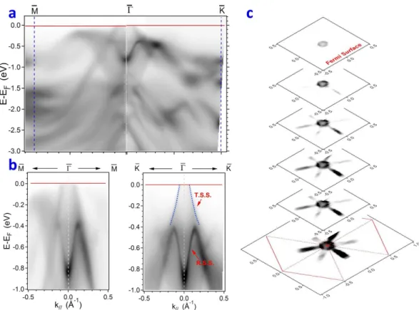
using high-resolution ARPES. Figure 1a displays the band structure of Sb2Te2Se(0001) on a large energy scale
along directions Γ − M and Γ − K; the spectra were recorded at photon energy 24 eV. In direction Γ − M, the BVB disperses toward the Fermi level in the middle of branch Γ − M. The band maximum of BVB about k// ~ 0.4 Å−1 was located near the Fermi level, but no band crossing at the Fermi level was observed in the analysis
of the momentum- distribution curves (MDC). In branch Γ − K, no component of the bulk band projection appeared in the range of the Fermi level and 0.35 eV. A ‘M’-shaped resonant surface state (RSS) about the Γ point similar to that in Sb2Te3 was observed in the bulk band gap within the scale of binding energy 0.40 to 0.86 eV. The
topological surface state (TSS) appears at binding energy 0.40 eV and disperses toward the Fermi level with kF = 0.065 Å−1 extracted from the MDC. A sharp topological surface state with width of MDC about 0.047 Å−1 indicates that the band-mapping result shows a highly crystalline quality of the present samples. The entire meas-ured band structure agrees qualitatively with previously calculated results28,37 and behaves in a typical p-type
manner. In comparison with the band structure of Sb2Te320, the contribution of BVB of Sb2Te2Se around the Fermi
level in the middle of branch Γ − M in our result and calculation show a strongly suppressed behaviour. The calculated result shows also a slight contribution of BVB from the bulk band projection around the Fermi level at the Γ point; an ARPES experiment dependent on photon energy was conducted to examine the contribution of BVB around the Γ point. We noticed that the energy scale between the Fermi level and the TSS in our result dif-fers slightly from that in a preceding calculation.
Figure 1b displays the enlarged band structure about the Γ point along directions Γ − M and Γ − K. Along direction Γ − M, the maximum of the BVB in the middle of direction Γ − M approaches the Fermi level and has a band edge about binding energy 40 meV, which is determined from a series of energy distribution curves (EDC) about k// = 0.4 Å−1 (see Supplementary materials). Along direction Γ − K, the contribution from the BVB is
observed only below binding energy 0.35 eV. The topological surface state with a linear dispersion down to bind-ing energy 0.22 eV can be extracted from the result of fittbind-ing the MDC. To confirm the existence of the Dirac point, we performed a doping test with alkali-metal-doped Sb2Te2Se (see Supplementary materials). The TSS and
RSS were clearly moved to a large binding energy after deposition of potassium or caesium atoms in small propor-tions, which implied a n-doping effect from the alkali-metal atoms. Once the shift magnitude approached 83 meV, the doping effect became saturated; the TSS and RSS no longer moved toward the region of large binding energy. The band dispersion of TSS still shows a linear dispersion after doping with an alkali metal, but no crossing point is observed because of the saturation of the doping effect. The position of the Dirac point was determined at 237 meV above the Fermi level through an extrapolation of the linear dispersion of TSS. We recorded infrared (FTIR) spectra to detect the band gap in Sb2Te2Se. A band gap ~ 417 meV at 98 K was extracted from the
absorp-tion edge in the infrared spectrum (see Supplementary materials). This result indicates that an isolated Dirac cone with the Dirac point located at 237 meV above the Fermi level exists in the Sb2Te2Se compound. Our observation
shows also a consistency with the recent result of the Landau-level (LL) spectra in Sb2Te2Se35. Additionally, the
scattering from bulk carriers is strongly suppressed. Figure 1c shows plots of the photoemission intensity in momentum space with various constant energies at the Fermi level − 30, 60, 90, 120 and 150 meV; the spectra are recorded at photon energy 24 eV. Only a circular-like surface state is observed on the Fermi surface. At 30 and 60 meV, the bulk component appears in direction Γ − M and shows a three-fold symmetry. With increasing binding energy, a slight deformation of the TSS is observed in the images of constant energy mapping.
In the photoemission experiment, the normal component of electron wave vector k⊥ of the initial state is based
on a free-electron model in the final state38,
θ = + ⊥ k 2 ( cosm E V ) (1) kin 2 2 0
in which Ekin is the kinetic energy of the photoelectron and V0 is the inner potential. To examine the property of a
3D bulk valence band, we conducted an ARPES experiment dependent on photon energy in a range from 12 to 42 eV, to cross several periods of the Brillouin zone (BZ) in the kz direction if the inner potential is assumed to be V0 = 9.64 eV39. A k-space map in the bulk BZ plotted with varied photon energy at collecting angle ± 18° of the
detector was used to explore the kz dependence of TSS, RSS and bulk bands (see Supplementary materials). The electronic structure of Sb2Te3 was studied for comparison with the same Sb2Te2Se crystal. Figure 2a shows the
band-mapping results of ARPES spectra in Sb2Te3 (0001) alongdirectionΓ −K with photon energies 24, 22, 18
and 12 eV. The Rashba splitting in RSS is observed clearly in the plots at 22, 18 and 12 eV. The extracted kF ~ 0.065 Å−1 and vF of TSS ~2.32 eV Å are consistent with previous work on Sb2Te340. The connection between
TSS and BVB1 proposed in preceding work is seen also in the plot at 22 and 12 eV. Figure 2b shows band-mapping results of ARPES spectra in Sb2Te2Se (0001) in a series alongdirectionΓ −K with photon energies 24, 22, 18 and
12 eV. In contrast to the results of Sb2Te3 along direction Γ − K, BVB1 and TSS show only a weak interaction
about the Γ point from BVB1 in the range about 0.35 eV binding energy, as shown in plots at 22 and 18 eV. No altered band dispersion in TSS and RSS was observed in the experiment with varied photon energy, indicating a 2-D behavior. Other results dependent on photon energy show the same results as in Fig. 2 (see Supplementary materials). In the present data, the width of MDC in RSS is about 0.072 Å−1; this value is small, and no clear
split-ting of RSS is observed. These conditions imply only a weak spin-orbital interaction in the Sb2Te2Se compound;
the momentum resolution in the present data is insufficient to resolve the predicted Rashba splitting. The reason is a weak spin-orbital interaction in Sb2Te2Se compound because of light element Se41. Figure 2c displays EDC
Figure 1. Band mapping of Sb2Te2Se in a wide energy range using photon energy 24 eV. (a) Band structure
of Sb2Te2Se(0001) along directions Γ − M and Γ − K. (b) Enlarged band structure about the Γ point of (a,c)
Plots of photoemission intensity in momentum space at various constant energies at photon energy 24 eV. The order of slices from the top slice is the Fermi level, 30, 60, 90, 120 and 150 meV. Only a circular-like surface state is observed at the Fermi surface.
www.nature.com/scientificreports/
about the Γ point in a series with photon energies 24, 22 and 18 eV. An analysis of MDC and EDC near the Fermi level around the Γ point with 18, 22, 30 and 32 eV was conducted to examine the band crossing at the Fermi level. Except the TSS, no obvious bulk band disperses and crosses the Fermi level (see Supplementary materials). At photon energy 18 eV, a clear intensity between the surface state at the Γ point was observed, but the same intensity at the next BZ was not observed in the plots at 30 and 32 eV when we verified the period of the kz dependence (see Supplementary materials). For comparison with the result of the LL spectra35, no feature therein
was observed below sample bias 150 mV, indicating that the observation of the shaded area between the surface state in the plot of 18 eV might come from the bulk band projection, even though we found no clear band disper-sion around at the Γ point.
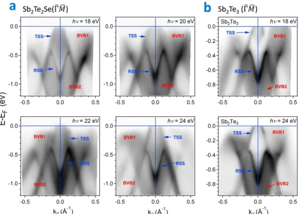
Figure 3a displays plots of the band-mapping results in Sb2Te2Se (0001) along directionΓ −M with photon
energies 18, 20, 22 and 24 eV. The bulk valence band disperses toward the Fermi level and has a band maximum about the middle of Γ − M. According to the analysis of MDC at the Fermi level and EDC with varied photon energy, no clear band crossing at the Fermi level is observed in a range covering 42 eV (see Supplementary mate-rials). Figure 3b shows plots of the band-mapping results in Sb2Te3 along Γ − M; these results are similar to those
reported18,19,40. The BVB1 in Sb
2Te3 has a clear band crossing at the Fermi level in the middle of Γ − M, which
indicates that scattering from bulk carriers is greater than that in the Sb2Te2Se compound. Regarding the
Figure 2. Comparison of the electronic structure of Sb2Te3 and Sb2Te2Se along dection Γ−K on a
photon-energy-dependent experiment. (a) Band-mapping results of ARPES in Sb2Te3 (0001) along direction Γ − K
with photon energies 24, 22, 18 and 12 eV. (b) Band-mapping results of ARPES in Sb2Te2Se (0001) along
direction Γ − K with photon energies 24, 22, 18 and 12 eV. (c) EDC about the Γ point in a series with photon energies 24, 22 and 18 eV.
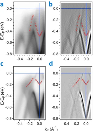
interaction of BVB and TSS about the Γ point, Fig. 4a,b display the photoemission intensity image of ARPES and the second derivative of the image in Sb2Te2Se respectively; these spectra were recorded at photon energy 22 eV.
The BVB1 band appears to have a crossing with the TSS band. This result implies an orbital hybridization that can occur about the Γ point to be similar to that in previous work on Sb2Te340. A comparison of the photoemission
intensity image in Sb2Te3 along direction Γ − M is shown in Fig. 4c,d. The Rashba splitting of TSS in Sb2Te3 is
clearly observed in the plot of the second derivative of the photoemission intensity image, but in our spectra no splitting in Sb2Te2Se can be resolved. Additionally, in contrast to Sb2Te3, because a major contribution of charge
carriers in Sb2Te2Se comes only from the BVB about the Γ point and because no other contribution is observed in
BZ, the resistivity in Sb2Te2Se is expected to be larger than that in Sb2Te3.
The dependence of resistivity on temperature and Hall measurement at room temperature were measured, showing the resistivity in Sb2Te2Se to be ten times that in Sb2Te3 (see Supplementary materials). The charge
car-rier number extracted from a Hall measurement near 296 K is 2.2 × 1020 cm−3 for Sb
2Te3 and 3.1 × 1019 cm−3 for
Sb2Te2Se. A charge carrier number ~ 3.1 × 1019 cm−3 in Sb2Te2Se indicates that it behaves as a heavily doped
semi-conductor, but the bulk carrier number in Sb2Te2Se still decreases significantly. These results show the consistency
of our ARPES result. Because the position of the Dirac point can be manipulated on controlling the chemical composition of a topological insulator in the bismuth family TIs, a possibility to decrease the charge carrier num-ber is to increase the content of Se atoms.
The efficiency of a thermoelectric cooler is generally described according to the value of the figure of merit, ZT, expressed as42,
σ κ = S
Z 2 (2)
in which S is thermopower, σ is electrical conductivity and κ is thermal conductivity. To consider a two-band model of a TI, the total thermopower and electrical conductivity come from the surface state and the bulk car-riers. The total electrical conductivity is expressible as σtotal = σbulk + σsurface; the total thermopower is expressed as Stotal = (σbulkSbulk + σsurfaceSsurface)/σtotal26. In a thin-film system, the contribution of electrical conductivity from bulk bands can be decreased on controlling the thickness of the TI. As Sb2Te3 behaves as a p-type semiconductor,
the maximum of the valence band is above the position of the Dirac point. The sign of the thermopower from the surface state and bulk are opposite if the position of the chemical potential is located above the Dirac point, which can result in a decreased thermopower. In contrast, more bulk carriers can increase the part of the thermal conductivity from the charge carriers if the position of the chemical potential is located below the Dirac point. Although the thermopower is increased, a greater thermal conductivity from bulk charged carriers confers no
Figure 3. Comparison of the electronic structures of Sb2Te2Se and Sb2Te3 along direction Γ−K on a
photon-energy-dependent experiment. (a) Band-mapping results of ARPES spectra in Sb2Te2Se (0001) along
direction Γ − M with photon energies 18, 20 22 and 24 eV. (b) Band-mapping results of ARPES in Sb2Te3(0001)
www.nature.com/scientificreports/
benefit to enhance the figure of merit. In our present Sb2Te2Se system, the maximum of the valence band is
sup-pressed inherently below the Fermi level, which implies the same sign of the thermopower for charge carriers from the surface state and from the bulk valence band. Sb2Te2Se has a high potential as a p-type thermoelectric
element, especially in an application of a hybrid thin-film heterostructure.
Robustness of a topological surface state.
Surface reactivity is a crucial problem for a TI in the bismuth family, such as Bi2Se3 and Bi2Te3. Previous work on the degradation of the surfaces of Bi2Se3 and Bi2Te3 shows thatthe doping level can be altered with gas or vapor contamination34,36,43–45; an extrinsic doping dependent on
ambi-ent environmambi-ental conditions in Sb2Te3 was also studied with Hall measurements46; this effect limits the potential
applications in TI in the bismuth family. In the present work, experiments involving the deposition of oxygen and an air environment were performed to detect the robustness of the topological surface state in Sb2Te2Se. Figure 5a
displays the resolution of core-level photoemission for a surface cleaved in situ and exposed to varied content of oxygen. No oxidation signal was observed after the deposition of oxygen about 1000 Langmuir (L) near 296 K. The band dispersions and the Fermi level-crossing vector of TSS and RSS before and after exposure were the same, which implies no impurity doping on the surface. Figure 5b displays the results of photoemission-mapping images after cleaving in situ in UHV and ex situ in an air environment. According to a comparison of these results, the image for the sample cleaved ex situ is only slightly smeared because of the surface pollution, but no change of the band position occurs, as shown in Fig. 5c. This result reveals the robustness of TSS in a Sb2Te2Se
compound and indicates that this Sb2Te2Se compound has a high potential for applications in spintronic devices.
In particular, the authors of a recent investigation proposed the possibility of tuning the doping level on varying the thickness of Sb2Te321. Further work on Sb2Te2Se becomes important.
Conclusion
For Sb2Te2Se single crystals of high quality that we grew, we studied the electronic structure of the Sb2Te2Se
com-pound with ARPES. The results of band mapping reveal that this Sb2Te2Se compound is a p-type semiconductor
and has an isolated Dirac cone. That the maximum of the bulk valence band in the middle of Γ − M is suppressed below the Fermi level implies a possibility of decreased scattering from that bulk valence band and that the ther-mopower can have the same sign for the surface state and the bulk carriers; the Sb2Te2Se system is hence a
Figure 4. High-resolution ARPES near the Fermi level in Sb2Te2Se and Sb2Te3 at photon energy 22 eV.
(a) Photoemission intensity image of ARPES in Sb2Te2Se(0001) recorded at photon energy 22 eV. (b) Second
derivative plot of (a,c), Photoemission intensity image of ARPES in Sb2Te3(0001) recorded at photon energy
potential candidate for the future application of spintronic and thermoelectric devices. More importantly, the robustness of TSS in the Sb2Te2Se system benefits the control of the performance of the devices.
Methods
Crystal growth.
Single crystals of Sb2Te2Se and Sb2Te3 were grown in a home-made resistively heatedfloat-ing-zone furnace (RHFZ). The initial raw materials Sb2Te2Se and Sb2Te3 were mixed according to the
stoichiomet-ric ratios. The stoichiometstoichiomet-ric mixtures of highly pure elements Sb (99.995%), Se (99.995%) and Te (99.995%) were first melted at 850~950 °C and cooled to about 23 °C afterward in an evacuated silica tube. The material was used as a feeding rod for the following RHFZ experiment. The growth rate was 1.5 mm/h. After growth, the crystals
Figure 5. Robustness of TSS in oxygen and atmospheric environments. (a) Core-level spectra of Sb2Te2Se
after deposition of oxygen. (b) Comparison of photoemission plots recorded at 24 eV for samples cleaved in situ in UHV and cleaved ex situ in air. (c) Comparison of EDC in the normal emission and MDC at the Fermi level. The feature of RSS becomes broadened but the peak position is constant. The same values of kF extracted from MDC for both cleaving conditions implies that no impurity doping occurs for a sample cleaved in an atmospheric environment.
www.nature.com/scientificreports/
were cooled to 23 °C over 50 h. Crystals of diameter 3.0 mm and length 30 mm were obtained reproducibly. A crystal cleaved along the basal plane showed a silvery, shiny, mirror-like surface.
ARPES.
ARPES were measured at National Synchrotron Radiation Research Center in Hsinchu, Taiwan at beamline BL21B1 U9-CGM for spectroscopy. The photoemission spectra were measured in a UHV chamber equipped with a hemispherical analyzer (Scienta R4000, collecting angle ± 15°). The polarization vector was invariably in the angular dispersive plane. The single crystals were cleaved in situ and measured at a base pressure 5.1 × 10⁻¹¹ Torr. All spectra were recorded for samples at 83 K and with varied photon energy. The angularresolu-tion was 0.2°; the energy resoluresolu-tion was better than 25 meV over the entire range of photon energy.
Regarding a test of the robustness of the topological surface state, single crystals of Sb2Te2Se were cleaved ex
situ in air, followed by transfer to the load-lock chamber after 5 min. After pumping for 1 h, the cleaved crystal was transferred to the analysis chamber for the ARPES experiment.
References
1. Chen, Y. L. et al. Massive Dirac fermion on the surface of a magnetically doped topological insulator. Science 329, 659–662 (2010). 2. Franz, M. et al. In praise of exact quantization. Science 329, 639–640 (2010).
3. Hsieh, D. et al. A tunable topological insulator in the spin helical Dirac transport regime. Nature 460, 1101–1105 (2009). 4. Hasan, M. Z. & Kane, C. L. Colloquium: topological insulators. Rev. Mod. Phys. 82, 3045 (2010).
5. Morre, J. E. The birth of topological insulators. Nature 464, 194–198 (2010)
6. Qi, X. L. & Zhang, S. C. Topological insulators and superconductors. Rev. Mod. Phys. 85, 1057 (2011). 7. Qi, X.-L. et al. Topological field theory of time-reversal invariant insulators. Phys. Rev. B 78, 195424 (2008).
8. Fu, L. & Kane, C. L. Superconducting proximity effect and Majorana fermions on the surface of a topological insulator. Phys. Rev.
Lett. 100, 096407 (2008).
9. Kimura, T. et al. Room-temperature reversible-spin Hall effect, Phys. Rev. Lett. 98, 156601 (2007). 10. Wolf, S. A. et al. Spintronics: a spin-based electronics vision for the future. Science 294, 1488–1495 (2001).
11. Hsieh, D. et al. Observation of unconventional quantum spin textures in topological insulators. Science 323, 919–922 (2009). 12. Zhang, H. et al. Topological insulators in Bi2Se3, Bi2Te3 and Sb2Te3 with a single Dirac cone on the surface. Nature Physics 5, 438–442
(2009).
13. Butch, N. P. et al. Strong surface scattering in ultrahigh-mobility Bi2Se3 topological insulator crystals. Phys. Rev. B 81, 241301 (R)
(2010).
14. Eto, K. et al. Angular-dependent oscillations of the magnetoresistance in Bi2Se3 due to the three-dimensional bulk Fermi surface. Phys. Rev. B 81, 195309 (2010).
15. Scablon, D. O. et al. Controlling bulk conductivity in topological insulators: key role of anti-site defects. Adv. Mater. 24, 2154–2158 (2012).
16. Wang, L. L. et al. Native defects in tetradymite Bi2(TexSe3−x) topological insulators. Phys. Rev. B 87, 125303 (2013).
17. Hsieh, D. et al. Observation of time-reversal-protected single-Dirac-cone topological-insulator states in Bi2Te3 and Sb2Te3. Phys. Rev. Lett. 103, 146401 (2009).
18. Seibel, C. et al. Single Dirac cone on the Cs-covered topological insulator surface Sb2Te3 (0001). Phys. Rev. B 86, 161105 (2012).
19. Plucinski, L. et al. Electronic structure, surface morphology, and topologically protected surface states of Sb2Te3 thin films grown on
Si(111). J. Appl. Phys. 113, 053706 (2013).
20. Johannsen, J. C. et al. Engineering the topological surface states in the (Sb2)m-Sb2Te3 (m = 0–3) superlattice series. Phys. Rev. B 91, 201101 (R) (2015).
21. M. Eschbach et al. Realization of a vertical topological p–n junction in epitaxial Sb2Te3/Bi2Te3heterostructures, Nature Comm. 6,
8816 (2015).
22. Hicks, L. et al. Use of quantum-well superlattices to obtain a high figure of merit from non-conventional thermoelectric materials.
Appl. Phys. Lett. 63, 3230–3232 (1993).
23. Boulouz, A. et al. Transport properties of V–Vi semiconducting thermoelectric BiSbTe alloy thin films and their application to micromodule Peltier devices. J. Appl. Phys. 89, 5009 (2001).
24. Peranio, N. et al. Structural and thermoelectric properties of epitaxially grown Bi2Te3 thin films and superlattices. J. Appl. Phys. 100,
114306 (2006).
25. Zastrow, S. et al. Thermoelectric transport and Hall measurements of low-defect Sb2Te3 thin films grown by atomic layer deposition. Semicond. Sci. Technol. 28, 035010 (2013).
26. Hinsche, N. F. et al. Impact of the topological surface state on the thermoelectric transport in Sb2Te3 thin films. ACS Nano 9,
4406–4411 (2015).
27. Zhang, W. et al. First-principle studies of three-dimensional strong topological insulators Bi2Te3, Bi2Se3 and Sb2Te3. New Journal of Physics 12, 065013 (2010).
28. Lin, H. et al. An isolated Dirac cone on the surface of ternary tetradymite-like topological insulators. New Journal of Physics 13, 095005 (2011).
29. Neupane, M. et al. Topological surface states and Dirac point tuning in ternary topological insulators. Phys. Rev. B 85, 235406 (2012).
30. Taskin, A. A. et al. Observation of Dirac holes and electrons in a topological insulator. Phys. Rev. Lett. 107, 016801 (2011). 31. Ren, Z. et al. Optimizing Bi2-xSbxTe3-ySey solid solutions to approach the intrinsic topological insulator regime. Phys. Rev. B 84,
165311 (2011).
32. Arakane, T. et al. Tunable Dirac cone in the topological insulator Bi2-xSbxTe3-ySey. Nature Comm. 3, 636 (2012).
33. Ren, Z. et al. Large bulk resistivity and surface quantum oscillations in the topological insulator Bi2Te2Se. Phys. Rev. B 82, 241306 (R) (2010).
34. Chen, C. et al. Robustness of topological order and formation of quantum well states in topological insulators exposed to ambient environment. Proc. Natl. Acad. Sci. USA 109, 3694 (2012).
35. Fu, Y. et al. Observation of Zeeman effect in topological surface state with distinct material dependence. Nature Comm. 7, 10829 (2016).
36. Park, S. R. et al. Quasiparticle scattering and the protected nature of the topological states in a parent topological insulator Bi2Se3. Phys. Rev. B 81, 041405 (R) (2010).
37. Men’shov, V. N. et al. Modeling near-surface bound electron states in a three-dimensional topological insulator: analytical and numerical approaches. J. Phys. Condensed Matter 26, 485003 (2014).
38. Damascelli, A. Probing the electronic structure of complex systems by ARPES. Physica Scripta T109, 61–74 (2004).
39. Tanaka, Y. et al. Evolution of electronic structure upon Cu doping in the topological insulator Bi2Se3, Phys. Rev. B 85, 125111 (2012).
40. Seibel, C. et al. Connection of a topological surface state with the bulk continuum in Sb2Te3 (0001). Phys. Rev. Lett. 114, 066802
41. Eremeev, S. V. et al. The effect of van der Waals gap expansions on the surface electronic structure of layered topological insulators.
New Journal of Physics 14, 113030 (2011)
42. Goldsmid, H. J. Thermoelectric Refrigeration (Plenum Press, New York USA 1964).
43. Benia, H. M. et al. Reactive chemical doping of the Bi2Se3 topological insulator, Phys. Rev. Lett. 107, 177602 (2011).
44. Golyashov, V. A. et al. Inertness and degradation of (0001) surface of Bi2Se3 topological insulator. J. Appl. Phys. 112, 113702 (2012).
45. Yashina, L. V. et al. Negligible surface reactivity of topological insulators Bi2Se3 and Bi2Te3 towards oxygen and water. ACS Nano 7,
5181–5191 (2013).
46. Kong, D. et al. Ambipolar field effect in the ternary topologicalinsulator (BixSb1−x)2Te3 by composition tuning. Nat. Nanotech. 6 705
(2011).
Acknowledgements
This work was supported by National Science Council of Taiwan under grant NSC 102-2112-M-213-003 and Ministry of Science and Technology of Taiwan under grants MOST 104-2112-M-110-012-MY2, 103-2119-M-110-003- MY3, 105-2911-I-009-509 and 103-2628-M-009-002-MY3, and in part by Bulgarian Science Fund, project FNI-T-02/26. The National Synchrotron Radiation Research Center (NSRRC) is operated under the Ministry of Science and Technology of Taiwan. CMC thanks Dr. Tun-Wen Pi and Dr. Je-Wei Lin at NSRRC for assisting photoemission and transport measurement and Dr. Chien-Ming Tu at NCTU for assisting recording of infrared spectra.
Author Contributions
C.M.C. and C.K.L. designed and performed the experiments. M.M.C.C. and S.H.Y. were in charge of preparing single crystals. C.M.C., S.C.W., W.C.C. and K.D.T. measured XRD, transport and ARPES. C.W.C., L.W.T. and C.K.L. contributed to the Raman experiments. C.W.L. and M.M.G. contributed to the robustness collection and FTIR measurement. C.M.C., C.K.L., M.M.C.C. and H.D.Y. contributed to scientific discussion. C.M.C., C.K.L and M.M.C.C. conceived the experiments and wrote the manuscript. C.K.L. supervised the project and reviewed the manuscript. All authors assisted in the manuscript preparation.
Additional Information
Supplementary information accompanies this paper at http://www.nature.com/srep Competing financial interests: The authors declare no competing financial interests.
How to cite this article: Lee, C.-K. et al. Robustness of a Topologically Protected Surface State in a Sb2 Te2 Se
Single Crystal. Sci. Rep. 6, 36538; doi: 10.1038/srep36538 (2016).
Publisher's note: Springer Nature remains neutral with regard to jurisdictional claims in published maps and
institutional affiliations.
This work is licensed under a Creative Commons Attribution 4.0 International License. The images or other third party material in this article are included in the article’s Creative Commons license, unless indicated otherwise in the credit line; if the material is not included under the Creative Commons license, users will need to obtain permission from the license holder to reproduce the material. To view a copy of this license, visit http://creativecommons.org/licenses/by/4.0/