• 沒有找到結果。

High-detectivity GaN MSM photodetectors with low-temperature GaN cap layers and Ir/Pt contact electrodes

N/A
N/A
Protected

Academic year: 2022

Share "High-detectivity GaN MSM photodetectors with low-temperature GaN cap layers and Ir/Pt contact electrodes"

Copied!
4
0
0

加載中.... (立即查看全文)

全文

(1)

High-Detectivity GaN MSM Photodetectors with Low-Temperature GaN Cap Layers and Ir/Pt Contact Electrodes

Chia-Lin Yu, a Ping-Chuan Chang, b,z Shoou-Jinn Chang, a and San-Lein Wu c

a

Institute of Microelectronics and Department of Electrical Engineering, National Cheng Kung University, Tainan 701, Taiwan

b

Department of Electronic Engineering, Nan Jeon Institute of Technology, Yen-Hsui Township, Tainan County 737, Taiwan

c

Department of Electronic Engineering, Cheng Shiu University, Kaohsiung 830, Taiwan

GaN-based metal-semiconductor-metal 共MSM兲 UV photodetectors 共PDs兲 with a low-temperature 共LT兲 GaN cap layer and Ir/Pt contact electrodes were fabricated. Compared with the conventional Ni/Au contacts, we found that Ir/Pt contacts can reduce the dark current. Further, a smaller dark current and larger UV-to-visible rejection ratio obtained from the PD with LT GaN cap layer and Ir/Pt contact electrodes were determined. Furthermore, the noise equivalent power and detectivity 共D

*

兲 were respectively obtained as 2.75 ⫻ 10

−13

W and 1.76 ⫻ 10

12

cm Hz

0.5

W

−1

for the aforementioned PDs.

© 2007 The Electrochemical Society. 关DOI: 10.1149/1.2718393兴 All rights reserved.

Manuscript submitted December 18, 2006; revised manuscript received January 26, 2007.

Available electronically March 26, 2007.

Recently, we have witnessed a great progress in III-nitride semi- conductors. With wide direct bandgap and high saturation velocity, III-nitride materials can be used for varieties of optical and elec- tronic devices.

1-3

In fact, high-performance III-nitride short- wavelength light-emitting diodes 共LEDs兲 were already successfully commercialized.

1,2

In addition, III-nitride materials are also useful for solar-blind UV photodetectors 共PDs兲 with various commercial and military applications. To date, several groups have reported promising results for GaN-based UV PDs with various structures such as p-n junction diodes, p-i-n PDs, Schottky barrier PDs, and metal-semiconductor-metal 共MSM兲 PDs.

4-7

Compared with bipolar PDs, the fabrication process of MSM PDs is much simpler. How- ever, the reverse bias leakage current in a Schottky barrier junction diode is expected to be significantly higher than in a bipolar junction diode.

8,9

Dark current is an important parameter to consider for PD applications. Therefore, the dark current of the devices must be sup- pressed first before high-performance MSM PDs can be realized.

To reduce the leakage current in MSM PDs, we need to enhance the Schottky barrier height at the metal/semiconductor interface. To achieve a large Schottky barrier height on GaN, one can choose metals with high work functions, such as Pt 共5.65 eV兲,

10

Ni 共5.15 eV兲,

11

and Pd 共5.12 eV兲.

12

However, many of the high-work- function metals have been shown to be unstable at high tempera- tures. This is believed to be caused by severe interdiffusion.

13

Pre- viously, it has been reported that iridium 共Ir, 5.46 eV兲 could form thermally stable Schottky contact on AlGaN/GaN heterostructure.

14

GaN-based UV MSM PDs with IrO

2

and Schottky diodes with oxi- dized Ir/Ni Schottky contacts were also demonstrated.

15,16

Alterna- tively, the reduction of leakage current may also be achieved via the addition of an insulating gate layer by adopting a metal-insulator- semiconductor 共MIS兲 structure.

17,18

To our knowledge, low- temperature 共LT兲 GaAs layer has ever been attempted in GaAs- based field transistors for the purpose of reducing gate leakage.

19

For GaN-based devices, it has also been shown that one can signifi- cantly reduce the leakage current and achieve a much larger photo- current to dark current contrast ratio by introducing a LT GaN on top of the conventional nitride UV PDs.

20

Keeping these advantages in mind, we hereby report the fabrication of nitride-based MSM PDs with LT GaN cap layers and Ir/Pt metal contacts. A detailed study on the properties of these MSM PDs is also discussed.

Samples used in this study were all grown by metallorganic chemical vapor deposition 共MOCVD兲 on c-face sapphire 共0001兲 substrates. Details of the growth conditions could be found else-

where. After annealing the sapphire substrate at 1100°C in H

2

am- bient to remove surface contamination, a 30 nm thick GaN nucle- ation layer grown at 600°C was deposited on the sapphire substrate.

On top of the nucleation layer, a 2 ␮m thick undoped GaN layer and a 30 nm thick 600°C-grown LT GaN cap layer were then epitaxially deposited 共i.e., sample I兲. Sheu et al.

21

demonstrated that the LT GaN behaves like an insulator with a large sheet resistivity. For comparison, samples without the LT GaN cap layer 共i.e., sample II兲 were also prepared. From the Hall measurement, it was found that the electron concentration of the sample II was ⬃10

17

cm

−3

.

Next, MSM PDs were fabricated based on these two structures.

Standard photolithography and liftoff were implemented for the fab- rication of GaN-based MSM UV PDs. Ni 共10 nm兲/Au 共20 nm兲 and Ir 共10 nm兲/Pt共20 nm兲 contact electrodes were evaporated onto sample II 共i.e., PDគA and PDគB, respectively兲 for fabricating the conventional GaN-based MSM UV PDs. Similarly, Ir/Pt and Ni/Au contact electrodes with same thicknesses were also deposited onto sample I 共i.e., PDគC and PDគD, respectively兲. The fingers of the contact electrodes are 14 ␮m wide, 100 ␮m long, and spaced by 6 ␮m apart. In this study, we kept the active area of fabricated PDs to be 100 ⫻ 234 ␮m. The room temperature current-voltage 共I-V兲 curves of these devices were then measured by using an HP 4145 semiconductor parameter analyzer under conditions of dark and light illumination. The top-illuminated spectral responsivity of these devices was also quantified using a Xe arc lamp with a calibrated monochromator as the light source. The monochromatic light, cali- brated with an optical power meter, was collimated onto each PD via an optical fiber. The noise characteristics were measured using a low-noise current preamplifier equipped with a fast Fourier trans- form 共FFT兲 spectrum analyzer.

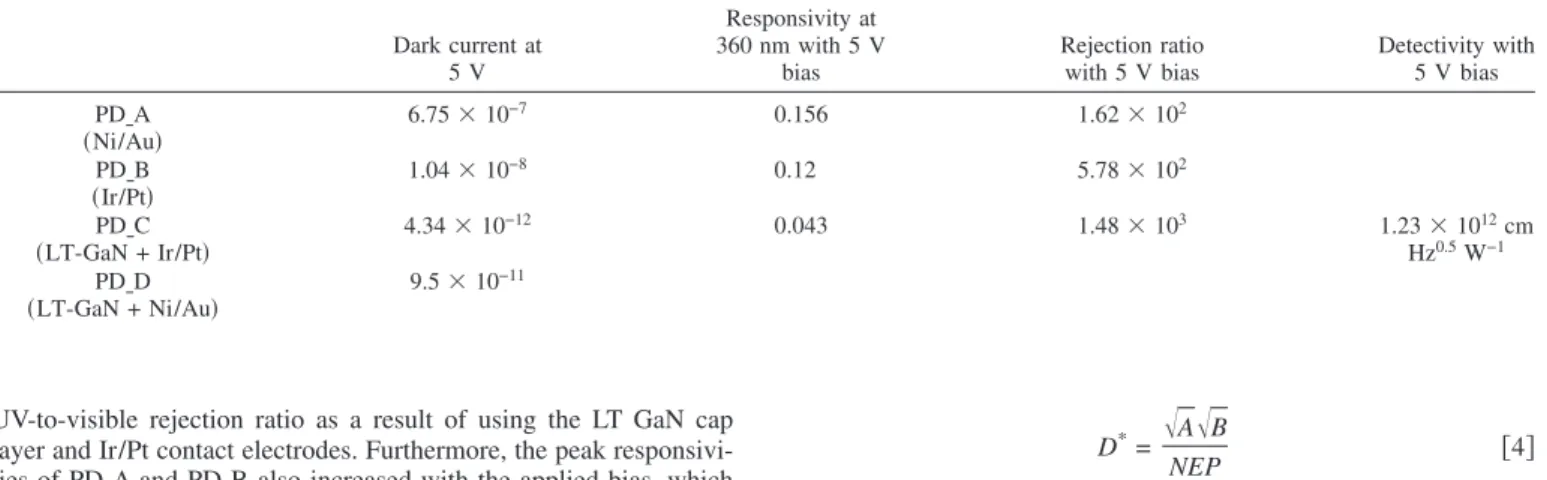
Figure 1 shows the measured I-V characteristics of the four MSM PDs. It could be seen that the dark current of PD គC is the lowest, while that of PD គA is the highest. Compared with PDគA, the PD គB exhibited smaller dark current, which is because the work function of Ir is larger than that of Ni. It is also possible that the metal-induced gap states 共MIGS兲 are less pronounced for PDគB,

22

which explains the finding of smaller dark current for PD គB. It was also demonstrated that a significant reduction in dark current was achievable through the use of an additional LT GaN cap layer, chiefly responsible for a much smaller dark current observed for PD គC and PDគD. In fact, this result can be attributed to a thicker and higher potential barrier and large series resistance due to the inser- tion of the highly resistive LT GaN cap layer. Hence, the dark cur- rent for a given bias was reduced. It was also observed that the dark current of PD គC was smaller than that of PDគD, which is again attributed to the presence of fewer MIGS. Compared with the con-

z

E-mail: [email protected]

Electrochemical and Solid-State Letters, 10 共6兲 H171-H174 共2007兲

1099-0062/2007/10共6兲/H171/4/$20.00 © The Electrochemical Society H171

Downloaded 11 Nov 2009 to 140.116.208.53. Redistribution subject to ECS license or copyright; see http://www.ecsdl.org/terms_use.jsp

(2)

ventional PD គA, smaller leakage current is observed with PDគC, which is the consequence of using a LT GaN cap layer and Ir/Pt contact electrodes.

Figure 2 depicts the measured photocurrents of the four fabri- cated PDs. The measured photocurrents of PD គC and PDគD were smaller than those of PD គA and PDគB, which is probably due to the photogenerated carriers compensated by the traps in the LT GaN layer. The photocurrents of PD គA and PDគB exhibited a slight de- pendency on voltage at higher voltages; however, this behavior was not observed for PD គC and PDគD. This result indicates the occur- rence of internal gain for PD គA and PDគB. The possible origin of the internal gain is the increased electron injection at the cathode con- tacts due to the lowering of the barrier height by the trapping of holes at the surface sites.

6

If this is the case, our result implies the effective passivation of surface states of the undoped GaN layer as a result of inserting a LT GaN layer.

23,24

In addition, we also found that the photocurrents of PDs with Ir/Pt were comparably smaller than that of PDs with Ni/Au due to the lower transmittance of Ir/Pt, as shown in the inset of Fig. 2.

Figures 3a-c show room temperature spectral responses of the PD គA, PDគB, and PDគC under various applied biases, respectively.

Notice that the photoresponses are relatively flat over the short- wavelength spectrum, while cutoff occurs at ⬃360 nm 共i.e., 3.4 eV for GaN bandgap 兲 for all PDs. Such a spectral response is typical for the visible-blind UV PDs. Furthermore, the transition region of PD គC appeared to be wider than PDគA and PDគB. The much wider transition region was due to the presence of deep-level-related trap states within the LT GaN cap layer, which had the tendency to absorb photons with energy lower than GaN bandgap energy. Pho- tons in this wavelength region could still excite electrons from deep

levels to the conduction band or from the valence band to deep levels in PD គC. With 5 V applied bias and an incident light with the wavelength of 360 nm, the measured responsivities were 0.156, 0.12, and 0.043 A/W for PD គA, PDគB, and PDគC, respectively. The much smaller measured responsivity observed from PD គC could be explained by the fact mentioned above. Here, we define UV-to- visible rejection ratio as the responsivity measured at 360 nm over the responsivity measured at 450 nm. With this definition, the UV- to-visible rejection ratios at 5 V bias were estimated to be 1.62

⫻ 10

2

, 5.78 ⫻ 10

2

, and 1.48 ⫻ 10

3

for PD គA, PDគB, and PDគC, respectively. Therefore, this finding indicates an enhancement of the Figure 1. Dark I-V characteristics of the four fabricated PDs.

Figure 2. Photocurrent characteristics of the four fabricated PDs.

Figure 3. Spectral responses of the 共a兲 PDគA, 共b兲 PDគB, and 共c兲 PDគC.

H172 Electrochemical and Solid-State Letters, 10 共6兲 H171-H174 共2007兲 H172

Downloaded 11 Nov 2009 to 140.116.208.53. Redistribution subject to ECS license or copyright; see http://www.ecsdl.org/terms_use.jsp

(3)

UV-to-visible rejection ratio as a result of using the LT GaN cap layer and Ir/Pt contact electrodes. Furthermore, the peak responsivi- ties of PD គA and PDគB also increased with the applied bias, which indicated the possibility of internal gain for PD គA and PDគB. On the contrary, the measured responsivity of PD គC appeared substantially less in bias dependency. All of these observations are closely related to the fact mentioned above.

Figure 4 shows measured low-frequency noise spectra of the PD គC in the frequency range of 10 Hz to 100 kHz at 5 V bias. It was found that noise power density of PD គC exhibited a dependency on frequency. It is well known that the flicker noise is proportional to 1/f

, with ␣ generally close to unity 共the so-called 1/f noise兲. The flicker noise originating from trap states in the LT GaN layer may be the dominant noise component for PD គC, which can be fitted by

S

n

共f兲 = K

f

关1兴

where S

n

共 f兲 is the spectral density of the current noise power, and K and ␣ are two fitting parameters. From the noise spectra shown in Fig. 4, it was found that ␣ and K extracted for PDគC were 1.14 and 5.19 ⫻ 10

−29

, respectively, throughout the measurement frequency range. The total noise current power can also be estimated by inte- grating S

n

共 f兲 over the frequency range

具i

n

2

=

S

n

共f兲df 关2兴

The noise equivalent power 共NEP兲 of the PD can also be calculated by

NEP =

具i

n

2

R 关3兴

where R is the responsivity of the PD. The normalized detectivity, D

*

, is then determined by

D

*

=

A

B

NEP 关4兴

where A is the area of the PD and B is the bandwidth. For a given bandwidth of 1 kHz and the detector area of 100 ⫻ 234 ␮m, the NEP and specific detectivity biased at 5 V could then be calculated accordingly. Using the noise spectra shown in Fig. 4, NEP and nor- malized detectivity, D

*

, were 2.75 ⫻ 10

−13

W and 1.76

⫻ 10

12

cm Hz

0.5

W

−1

for PD គC. In other words, we achieved the low NEP and the high normalized detectivity, D

*

, from PD គC. The D

*

and NEP of our PDs was much better than MSM and MIS PDs reported previously.

25,26

Table I shows the comparison of results from four PDs. These results suggest the performances of GaN- based MSM UV PDs can be effectively improved by incorporating a LT GaN cap layer and Ir/Pt contact electrodes.

In summary, GaN-based MSM UV PDs with a LT GaN cap layer and Ir/Pt contact electrodes were fabricated. We achieved smaller dark current and a larger UV-to-visible rejection ratio for the PD with LT GaN cap layer and Ir/Pt contact electrodes. We have also ascertained that the flicker noise may be the dominant noise compo- nent for the PD with a LT GaN cap layer and Ir/Pt contact elec- trodes. Furthermore, NEP and D

*

were correspondingly determined as 2.75 ⫻ 10

−13

W and 1.76 ⫻ 10

12

cm Hz

0.5

W

−1

for the GaN- based MSM UV with LT GaN cap layer and Ir/Pt contact electrodes.

Nan Jeon Institute of Technology assisted in meeting the publication costs of this article.

References

1. M. Mayer, A. Pelzmann, C. Kirchner, M. Schauler, F. Eberhard, M. Kamp, P.

Unger, and K. J. Ebeling, J. Cryst. Growth, 190, 782 共1998兲.

2. J. Han and A. V. Nurmikko, IEEE J. Sel. Top. Quantum Electron., 8, 289 共2002兲.

3. U. K. Mishra, Y. F. Wu, B. P. Keller, S. Keller, and S. P. Denbaars, IEEE Trans.

Microwave Theory Tech., 46, 756 共1998兲.

4. N. Biyikli, I. Kimukin, O. Aytur, and E. Ozbay, IEEE Photonics Technol. Lett., 16, 1718 共2004兲.

5. A. Osinsky, S. Gangopadhyay, R. Gaska, B. Williams, M. A. Khan, D. Kuksenkov, and H. Temkin, Appl. Phys. Lett., 71, 2334 共1997兲.

6. O. Katz, V. Garber, B. Meyler, G. Bahir, and J. Salzman, Appl. Phys. Lett., 79, 1417 共2001兲.

7. C. L. Yu, C. H. Chen, S. J. Chang, Y. K. Su, S. C. Chen, P. C. Chang, P. C. Chen, M. H. Wu, H. C. Chen, and K. C. Su, IEEE Photonics Technol. Lett., 17, 875 共2005兲.

8. D. V. Kuksenkov, H. Temkin, A. Osinsky, R. Gaska, and M. A. Khan, J. Appl.

Phys., 83, 2142 共1998兲.

9. A. P. Zhang, G. T. Dang, F. Ren, H. Cho, K. P. Lee, S. J. Pearton, J. I. Chyi, T. E.

Nee, C. M. Lee, and C. C. Chuo, IEEE Trans. Electron Devices, 48, 407 共2001兲.

10. S. N. Mohammad, Z. Fan, A. E. Botchkarev, W. Kim, O. Aktas, and A. Salvador, Electron. Lett., 32, 598 共1996兲.

11. J. D. Guo, F. M. Pan, M. S. Feng, R. J. Guo, P. F. Chou, and C. Y. Chang, J. Appl.

Phys., 80, 1623 共1996兲.

12. A. C. Schmitz, A. T. Ping, M. A. Khan, Q. Chen, J. W. Yang, and I. Adesida, Electron. Lett., 32, 1832 共1996兲.

13. E. Monroy, F. Calle, T. Palacios, J. Sanchez-Osorio, M. Verdu, F. J. Sanchez, M. T.

Montojo, F. Omnes, Z. Bougrioua, I. Moerman, and P. Ruterana, Phys. Status Solidi A, 188, 367 共2001兲.

14. C. M. Jeon, H. W. Jang, and J. L. Lee, Appl. Phys. Lett., 82, 391 共2003兲.

15. J. K. Kim, H. W. Jang, C. M. Jeon, and J. L. Lee, Appl. Phys. Lett., 81, 4655 共2002兲.

16. H. Jiang, T. Egawa, H. Ishikawa, Y. B. Dou, C. L. Shao, and T. Jimbo, Electron.

Table I. The comparison of results from different PDs.

Dark current at 5 V

Responsivity at 360 nm with 5 V

bias

Rejection ratio with 5 V bias

Detectivity with 5 V bias PD គA

共Ni/Au兲 6.75 ⫻ 10

−7

0.156 1.62 ⫻ 10

2

PD គB

共Ir/Pt兲 1.04 ⫻ 10

−8

0.12 5.78 ⫻ 10

2

PD គC

共LT-GaN + Ir/Pt兲 4.34 ⫻ 10

−12

0.043 1.48 ⫻ 10

3

1.23 ⫻ 10

12

cm

Hz

0.5

W

−1

PD គD

共LT-GaN + Ni/Au兲 9.5 ⫻ 10

−11

Figure 4. LF noise spectra of the PD គC.

H173 Electrochemical and Solid-State Letters, 10 共6兲 H171-H174 共2007兲 H173

Downloaded 11 Nov 2009 to 140.116.208.53. Redistribution subject to ECS license or copyright; see http://www.ecsdl.org/terms_use.jsp

(4)

Lett., 39, 1604 共2003兲.

17. S. J. Chang, Y. K. Su, Y. Z. Chiou, J. R. Chiou, B. R. Huang, C. S. Chang, and J.

F. Chen, J. Electrochem. Soc., 150, C77 共2003兲.

18. C. T. Lee, H. W. Chen, and H. Y. Lee, Appl. Phys. Lett., 82, 4304 共2003兲.

19. L. W. Yin, Y. Hwang, J. H. Lee, R. M. Kolabas, R. J. Trew, and U. K. Mishra, IEEE Electron Device Lett., 11, 561 共1990兲.

20. M. L. Lee, J. K. Sheu, W. C. Lai, Y. K. Su, S. J. Chang, C. J. Kao, C. J. Tun, M.

G. Chen, W. H. Chang, G. C. Chi, and J. M. Tsai, J. Appl. Phys., 94, 1753 共2003兲.

21. J. K. Sheu, M. L. Lee, and W. C. Lai, Appl. Phys. Lett., 86, 052103 共2005兲.

22. E. H. Rhoderick and R. H. Williams, Metal-Semiconductor Contacts, 2nd ed., Oxford University Press, New York 共1988兲.

23. J. C. Carrano, T. Li, P. A. Grudowski, C. J. Eiting, R. D. Dupuis, and J. C.

Campbell, J. Appl. Phys., 83, 6148 共1998兲.

24. V. Adivarahan, G. Simin, J. W. Yang, A. Lunev, and M. A. Khan, Appl. Phys. Lett., 77, 863 共2000兲.

25. Y. Z. Chiou, J. Electrochem. Soc., 152, G639 共2005兲.

26. E. Monroy, F. Calle, J. L. Pau, E. Munoz, and F. Omnes, Electron. Lett., 36, 2096 共2000兲.

H174 Electrochemical and Solid-State Letters, 10 共6兲 H171-H174 共2007兲 H174

Downloaded 11 Nov 2009 to 140.116.208.53. Redistribution subject to ECS license or copyright; see http://www.ecsdl.org/terms_use.jsp

數據

Figure 2 depicts the measured photocurrents of the four fabri- fabri-cated PDs. The measured photocurrents of PD គC and PDគD were smaller than those of PD គA and PDគB, which is probably due to the photogenerated carriers compensated by the traps in the LT
Figure 4 shows measured low-frequency noise spectra of the PD គC in the frequency range of 10 Hz to 100 kHz at 5 V bias

參考文獻

相關文件

• Contact with both parents is generally said to be the right of the child, as opposed to the right of the parent. • In other words the child has the right to see and to have a

Nowadays Nan-Gan Island and Bei-Gan Island are in Matsu archipelago called Gan-Tang-Shan by Ming Dynasty. Gan-Tang-Shan located on the sea out Min-Jiang estuary in Fu-Jian Province

For large-cap stocks (quintiles 1 and 2), the autoquote instrument shows that an increase in algorithmic liquidity supply narrows both the quoted and effective spread.. To interpret

• Zhen Yang, Wei Chen, Feng Wang, Bo Xu, „Improving Neural Machine Translation with Conditional Sequence Generative Adversarial Nets“, arXiv 2017. • Supervised

Li, Shaoting Zhang, Xiaogang Wang, Xiaolei Huang, Dimitris Metaxas, “StackGAN: Text to Photo-realistic Image Synthesis with Stacked Generative Adversarial Networks”, ICCV,

Biases in Pricing Continuously Monitored Options with Monte Carlo (continued).. • If all of the sampled prices are below the barrier, this sample path pays max(S(t n ) −

• We need to make each barrier coincide with a layer of the binomial tree for better convergence.. • The idea is to choose a Δt such

Abstract—We propose a multi-segment approximation method to design a CMOS current-mode hyperbolic tangent sigmoid function with high accuracy and wide input dynamic range.. The