P-contact metal oxide in efficient organometal halide perovskite/fullerene hybrid solar cells
Jun-Yuan Jeng
1, Kuo-Cheng Chen
1, Tsung-Yu Chiang
1, Pei-Ying Lin
1, Tzung-Da Tsai
1, Yun-Chorng Chang
1, Tzung-Fang Guo
1,2 a), and Peter Chen
1,2,3b)1 Department of Photonics
2 Advanced Optoelectronic Technology Center
3 Research Center for Energy Technology and Strategy National Cheng Kung University
Tainan, Taiwan 701, ROC
Ten-Chin Wen
Department of Chemical Engineering National Cheng Kung University
Tainan, Taiwan 701, ROC
Yao-Jane Hsu
National Synchrotron Radiation Research Center Hsinchu, Taiwan 300, ROC
Abstract
Applying a thin nickel oxide (NiO
x) interlayer between glass/indium-tin-oxide (ITO) electrode and light absorbing methylammonium lead iodide (CH
3NH
3PbI
3) perovskite significantly increases the photovoltaic performance of perovskite/fullerene-derivative planar-heterojunction (PHJ) hybrid solar cells. First, NiO
xelectrode interlayer is a p-type semiconductor of high work function of 5.4 eV, which is close to the valence band edge level of CH
3NH
3PbI
3perovskite (5.4 eV). The alignment of energy level minimizes the interfacial energy losses for the hole transfer and optimizes the photovoltage output of device. Second, CH
3NH
3PbI
3perovskite
a)
Author to whom all correspondence should be addressed; electronic mail: [email protected]
b)
Author to whom all correspondence should be addressed; electronic mail: [email protected]
films prepared by the spin-coating process on glass/ITO/NiO
xsubstrate exhibit a relatively smooth morphology than those deposited on glass/ITO/poly(3,4-ethylenedioxythiophene) poly(styrene-sulfonate) (PEDOT:PSS) substrate. The conformal coverage of the perovskite film enhances the light harvesting, reduces the leakage current, increases short-circuit current (J
SC), and elevates the power conversion efficiency (PCE) of the devices. The best performing cell with the configuration of glass/ITO/NiO
x/CH
3NH
3PbI
3perovskite/[6,6]-phenyl C61-butyric acid methyl ester (PCBM)/bathocuproine/Al presents an open-circuit voltage (V
OC)=
0.92 V, a J
SC= 12.43 mA/cm
2, and a fill factor (FF) = 0.68, corresponding to a PCE of 7.8 % under standard 1 sun AM 1.5G simulated solar irradiation. The performance is much superior to the device applying PEDOT:PSS interlayer with photovoltaic parameters of V
OC= 0.62 V, J
SC= 9.39 mA/cm
2, and fill factor FF = 0.66, corresponding to a PCE of 3.9 %. Our findings reveal the design principle for enhancing the photovoltaic performance of CH
3NH
3PbI
3perovskite/PCBM hybrid PHJ solar cells through the judicious selection of the metal oxide electrode interlayer.
Keywords: CH
3NH
3PbI
3, perovskite, planar heterojunction, hybrid solar cell, metal
oxide, nickel oxide, electrode interlayer
Organometal halide perovskite is an ideal photovoltaic material that exhibits a direct optical band gap around 1.5 eV, a low exciton bonding energy and long diffusion length (~1 µm), a broad range of light absorption covering the visible to near-infrared spectrum (800 nm) with high extinction coefficient (~10
4cm
-1at 550 nm)
1-3. Most importantly, organo-lead halide perovskites behave the ambipolar characteristics and work very well with organic carrier transport materials, such as 2,2’7,7’-tetrakis-(N,N-di-p-methoxyphenyl-amine)-9,9’-spirobifluorene
(spiro-OMeTAD)
4,5, fullerene (C
60) and [6,6]-phenyl C61-butyric acid methyl ester (PCBM)
6-11, and the conjugated polymers…etc.
12-14, to form a hybrid heterojunction and generate the efficient photovoltaic effect. Organometal halide perovskite-based mesoscopic or planar heterojunction (PHJ) solar cells present the very promising photovoltaic performance. Recent reports had indicated the devices based on this material showing the high power conversion efficiency (PCE) of 12~15%
4,5,12,15,16. Several reports prospectively propose the device can achieve PCE of 20% shortly.
17,18The hybrid PHJ perovskite-based solar cells have the advantage to be fabricated by low temperature and solution processes, and flexible devices with remarkable efficiency have been demonstrated recently.
8,9,19,20Our previous work had successfully demonstrated the efficient hybrid solar cells
made of the methylammonium lead iodide (CH
3NH
3PbI
3)/C
60PHJ configuration.
6Applying C
60derivatives of varied lowest unoccupied molecular level (LUMO)
modulates the open-circuit voltage (V
OC) as well as other device parameters. These
results verify the photovoltaic effect yielding from CH
3NH
3PbI
3perovskite/C
60hybrid
PHJ interface and reveal the difference in the energy level at junction interface would
be important parameters to manipulate the device performance. The hybrid
CH
3NH
3PbI
3/PCBM PHJ cell exhibits the decent photovoltaic performance as
reported in our previous study and the photovoltaic parameters of similar device
configurations were further improved by other related works.
6,8-11First, under the illumination, the electron transfer from excited states in CH
3NH
3PbI
3perovskite to PCBM is very efficient. Docampo et al. reported the quenching of the perovskite photoluminescence (PL) by PCBM is much completed, about 91%, than that of TiO
2(47%).
8The electron transfer process as calculated by Xing et al. is around 0.4 ns, which is faster than the transport of holes to spiro-OMeTAD, 0.66 ns.
1Second, the match of the LUMO level of PCBM (3.7 to 3.9 eV) with the conduction band (CB) edge level of CH
3NH
3PbI
3perovskite (3.9 eV) minimizes the energy redundancy to achieve the maximal photovoltage output of devices. These properties make PCBM an ideal electron acceptor material with CH
3NH
3PbI
3perovskite (donor) in a hybrid donor-acceptor PHJ. However, while considering the transfer and transport of holes from CH
3NH
3PbI
3perovskite to reach the positive charge collecting electrode, the mismatch 0.6 eV between the valence band level (VB) edge level of CH
3NH
3PbI
3perovskite, 5.4 eV, with the work function of indium-tin-oxide (ITO) electrode, 4.8 eV, markedly diminishes the photovoltage output. Accordingly, introducing an electrode interlayer to adjust the mismatch of the energy level would be an applicable approach to reduce the energy loss and elevate the photovoltaic efficiency.
Poly(3,4-ethylenedioxythiophene) poly(styrene-sulfonate) (PEDOT:PSS) is a
widely used electrode buffer to modify the surface properties of glass/ITO substrate
for most organic electronics devices, but researchers in this society are aware of many
drawbacks by using PEDOT:PSS interlayer, especially for devices under the
long-term operation
21-24. Irwin et al. first reported the replacement of PEDOT:PSS
layer by a thin p-type semiconducting nickel oxide (NiO) layer in polymer
bulk-heterojunction (BHJ) solar cells and got the enhanced device performance.
25Later, Steirer et al. developed a relatively simple solution process to deposit NiO
xthin
interlayer on glass/ITO electrode.
26Owing to the optical transparency, the chemical
stability, the good conductivity of hole, as well as the tunable work function from 5.0 to 5.6 eV by the different O
2-plasma surface treatments, consequently we would regard that NiO
xcan be the potential electrode interlayer to work with CH
3NH
3PbI
3perovskite materials. A better alignment in the work function of NiO
xelectrode interlayer with the VB edge level of CH
3NH
3PbI
3perovskite would improve the transfer of hole and increase device photovoltage as well as other photovoltaic parameters. Actually, applying NiO
xelectrode interlayer to enhance V
OCand PCE of BHJ solar cells made of low band gap conjugated materials had been reported by many researchers, due to a better match of the transfer level for hole in the highest occupied molecular orbital (HOMO) level of donor materials.
22,25-27In this manuscript, we apply a thin NiO
xelectrode interlayer on the glass/ITO electrode to fabricate the efficient CH
3NH
3PbI
3/PCBM PHJ hybrid solar cells. Our results indicate that all photovoltaic parameters exhibit a remarkable enhancement by applying the NiO
xelectrode interlayer. The hybrid cell of the configuration, glass/ITO/NiO
x/CH
3NH
3PbI
3perovskite/PCBM/bathocuproine (BCP)/Al, presents a V
OC= 0.92 V, a short-circuit current (J
SC) = 12.43 mA/cm
2, and a fill factor (FF) = 0.68, corresponding to a PCE of 7.8% under standard 1 sun AM 1.5G simulated solar irradiation. The photovoltaic parameters are superior to those of the hybrid cell with PEDOT:PSS interlayer of V
OC= 0.62 V, a J
SC= 9.39 mA/cm
2, and a fill factor FF = 0.66, corresponding to a PCE of 3.9 %. We attribute the match of energy level for the VB edge level of CH
3NH
3PbI
3perovskite with the work function of NiO
xminimize the energy loss for hole and optimize the magnitude of V
OC. The higher magnitude of J
SCand PCE also results from the better surface coverage (93%) of CH
3NH
3PbI
3perovskite film on the glass/ITO/NiO
xsubstrate. Our results point out the design
principle for applying a p-type, high work function, nickel oxide electrode interlayer
to fabricate CH
3NH
3PbI
3perovskite/PCBM PHJ hybrid cells, which is of great
importance to future research and development in the community of next generation stable and cost-viable photovoltaics.
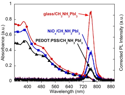
Figure 1 illustrates the UV-Vis spectra and the corrected PL responses of CH
3NH
3PbI
3perovskite film on the glass, glass/ITO/PEDOT:PSS, and glass/ITO/NiO
xsubstrate by a spin coating process. The magnitude of the steady-state PL response for CH
3NH
3PbI
3perovskite film from 700 to 830 nm was reduced by the PEDOT:PSS and NiO
xinterlayer in a bilayer structure, which indicates the compatibility of charge transfer from CH
3NH
3PbI
3perovskite to PEDOT:PSS and NiO
xlayers. The corrected PL responses of CH
3NH
3PbI
3perovskite layers on the glass, glass/NiO
x, and glass/PEDOT:PSS substrates are normalized to the light harvesting efficiency (LHE) with the relationship of LHE =1-10
-Absorbance. The results show that the differences in PL responses are not resulted from the absorption variance of CH
3NH
3PbI
3perovskite layers. This observation indicated NiO
xas expected is a potential electrode interlayer for the charge transfer of hole. Docampo et al. reported the similar PL quenching effect of CH
3NH
3PbI
3-xCl
xperovskite on PEDOT:PSS and NiO layers, too
8. However, while they applied CH
3NH
3PbI
3-xCl
xperovskite with p-type NiO electrode interlayer to fabricate the devices, Docampo et al. depicted that the devices present the very low photovoltaic performance, because of the extremely poor perovskite film formation upon the substrate and very poor surface coverage. This leads to the direct contact between PCBM n-type layer and the p-type metal oxide and generates a shunting path. They also pointed out the high series resistance of the device arising from the low conductivity of the p-type metal oxide layer is another concerning issue.
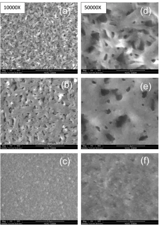
The crystal growth and aggregation of CH
3NH
3PbI
3or CH
3NH
3PbI
3-xCl
xperovskite during the spin coating process coarsen the films on the substrate and
markedly degrade device performance or result in device failure. To preheat a
glass/ITO/NiO
xsubstrate at an elevated temperature of 60 °C for 5 min and then to immediately cast the precursor solution at a high-spinning speed of 9500 rpm ensure the solvent evaporation of solution during the perovskite film formation in a fast regime to inhibit the coarsening of the crystals
6. Figure 2(a) to (c) illustrate the high-resolution scanning electron microscopy (HR-SEM) images at the magnification of 10,000x for CH
3NH
3PbI
3perovskite film on the glass/ITO/PEDOT:PSS (8000 rpm), glass/ITO/NiO
x(8000 rpm), and glass/ITO/NiO
x(9500 rpm) substrates, respectively. In Fig. 2(a), the CH
3NH
3PbI
3perovskite film exhibits densely interconnected crystalline strips on the glass/ITO/PEDOT:PSS substrate. The surface coverage of the film is estimated approximately 85%. Although the film looks very smooth and reflective as inspected by naked eye, there are still voids on the film, as shown in Fig. 2(d) HR-SEM image at the magnification of 50,000x, causing the shunting path of the devices. On the other hand, we observe that CH
3NH
3PbI
3perovskite films exhibit a different surface morphology and a higher surface coverage, 89%, on glass/ITO/NiO
xsubstrate as shown in Fig. 2(b). Increasing the spinning speed from 8000 rpm to 9500 rpm further improves the quality of CH
3NH
3PbI
3perovskite film formation as illustrated in Fig. 2(c), in which the number density of void or crevice on the film is markedly reduced. The surface coverage estimated from Figs. 2(c) is estimated approximately 93%. Figs. 2(c) and (f) indicate the images of a good quality of CH
3NH
3PbI
3perovskite film upon the flat NiO
xsurface (glass/ITO/NiO
xsubstrate). Our results are very different to the observation reported by Docampo et al., probably due to the differences in the film forming and preparing condition of perovskite materials and NiO
xlayer.
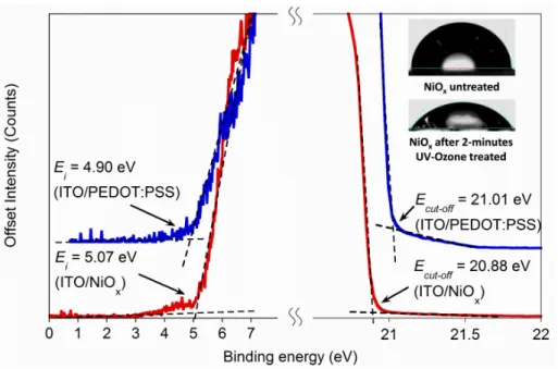
The UV-Ozone treatment of glass/ITO/NiO
xsubstrate for 2 minutes modifies the
work function and surface wetting properties of NiO
xelectrode interlayer. Figure 3
depicts the onset (E
i) and cutoff (E
cut-off) energy regions in Ultraviolet photoelectron
spectrum (UPS) (He I) of the surface measurement for the glass/ITO/PEDOT:PSS and the treated glass/ITO/NiO
xsubstrate. The E
iand E
cut-offenergy is 5.07 eV and 20.88 eV, respectively, and the work function (φ) of NiO
xelectrode interlayer is estimated to be 5.4 eV by equation φ = 21.21 –(E
cut-off-E
i). In addition, UV-Ozone treatment reduces the water contact angle of the glass/ITO/NiO
xsubstrate from 79° (untreated) to 58° (treated), in which the insets of Figure 3 show the photographs of the measurement. The decrease of the water contact angle improves the surface wetting property of NiO
xelectrode interlayer for precursor solution as well as the surface coverage of CH
3NH
3PbI
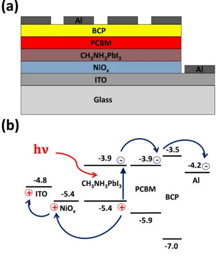
3perovskite film. Figure 4(a) illustrates the device configuration of glass/ITO/NiO
x/CH
3NH
3PbI
3perovskite/PCBM/BCP/Al and Figure 4(b) diagrams the energy level of each layer. As shown in Figure 4(b), both edge level of CB (3.9 eV) and VB (5.4 eV) in CH
3NH
3PbI
3perovskite exhibit a good alignment with LUMO level of PCBM (3.9 eV) and the work function of NiO
x(5.4 eV), respectively. Accordingly, it is anticipated that the minimal energy loss for the transfer of charge carriers (electron and hole) in the CH
3NH
3PbI
3perovskite/PCBM and NiO
x/CH
3NH
3PbI
3perovskite heterojunction interfaces enhances the photovoltage output of the hybrid solar cells. On the other hand, NiO
xis a wide band gap material with the CB edge level around -2.1 eV, which is much higher than that of perovskite around -3.9 eV, thus injection of electron into NiO
xis not energetically favorable.
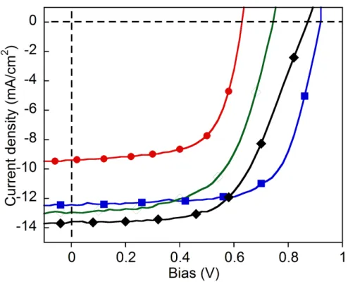
Figure 5(a) presents the current density-voltage (J-V) curves of hybrid organic
solar cells under the standard 1 sun AM 1.5G simulated solar irradiation, made of the
glass/ITO as the positive electrode, PEDOT:PSS or NiOx as the electrode interlayer, a
PHJ of CH
3NH
3PbI
3perovskite/PCBM as the active layers, a thin BCP film as
hole-blocking layer (HBL), and an Al negative electrode. Table I. summarizes the
photovoltaic parameters of the devices. The hybrid cell of the configuration,
glass/ITO/PEDOT:PSS/CH
3NH
3PbI
3perovskite (9500 rpm)/PCBM/BCP/Al, presents
a V
OC= 0.62 V, a J
SC= 9.39 mA/cm
2, and a fill factor FF = 0.66, corresponding to a
PCE of 3.9 %. On the other hand, the hybrid cell of the configuration,
glass/ITO/NiO
x/CH
3NH
3PbI
3perovskite (9500 rpm)/PCBM/BCP/Al, presents V
OC=
0.92 V, a J
SC= 12.43 mA/cm
2, and a fill factor (FF) = 0.68, corresponding to a PCE
of 7.8%, a superior photovoltaic performance than that of device applying
PEDOT:PSS interlayer. The change of V
OCis correlated with the work function of
electrode interlayer. The work function of glass/ITO/PEDOT:PSS is estimated to be
5.1 eV, by UPS measurement. The E
iand E
cut-offenergy is 4.90 eV and 21.01 eV,
respectively, and the φ = 21.21–(E
cut-off-E
i) = 5.1. The result from UPS measurement
indicates that the VB edge level (5.4 eV) of CH
3NH
3PbI
3perovskite exhibits a good
alignment with the work function of NiO
x(5.4 eV), but there is the 0.3 eV offset in
the PEDOT:PSS (5.1 eV)/CH
3NH
3PbI
3perovskite (5.4 eV) junction interface. The
increase in V
OCmagnitude from 0.62 V to 0.92V is related with the assumption that
minimizing the energy loss for hole in NiO
x/CH
3NH
3PbI
3perovskite junction elevates
the output photovoltage. Additionally, the CH
3NH
3PbI
3perovskite exhibits a better
surface coverage of film morphology on glass/ITO/NiO
x. The better surface coverage
of CH
3NH
3PbI
3perovskite film on the glass/ITO/NiO
xsubstrate reduces the shunting
path of devices. This would be another dominant parameter to the enhanced
magnitude of V
OC. At current stage, we cannot totally exclude the above two effects
on the photovoltaic performance. The increase of V
OCmay be further fortified by
analyzing Electrochemical Impedance Spectroscopy of devices, which is currently
under investigation. The hybrid cell of the configuration,
glass/ITO/NiO
x/CH
3NH
3PbI
3perovskite (8000 rpm)/PCBM/BCP/Al, presents V
OC=
0.88 V, a J
SC= 13.58 mA/cm
2, and a FF = 0.58, corresponding to a PCE of 6.9%. The
higher magnitude of J
SCprobably results from the relatively thicker CH
3NH
3PbI
3perovskite film prepared at 8000 rpm. The decreases of other photovoltaic parameters are associated with the lower surface coverage of CH
3NH
3PbI
3perovskite film.
Additionally, the hybrid cell of the configuration, glass/ITO/NiO
x/CH
3NH
3PbI
3perovskite (9500 rpm)/C
60/BCP/Al, is fabricated for comparison. The device presents a V
OC= 0.74 V, a J
SC= 12.95 mA/cm
2, and a FF = 0.60, corresponding to a PCE of 5.7%. The result indicates the energy loss for electron in CH
3NH
3PbI
3perovskite/C
60junction (C
60of a LUMO level 4.5 eV) also degrades the output device performance.
Another parameter to modulate the photovoltaic performance is the treatment of
glass/ITO/NiO
xsubstrate by UV-Ozone for fabrication. Table I. also presents the data
for the glass/ITO/NiO
x/CH
3NH
3PbI
3perovskite (8000 rpm)/PCBM/BCP/Al cells
without and with 2, or 4 minutes of UV-Ozone treatment on glass/ITO/NiO
x. Our
results agree with the observations by Park et al. and Steirer et al. that the variation of
the surface properties of NiO
xfilm modulates the photovoltaic parameters.
23,26The
hybrid cell fabricated with 2 minutes of UV-Ozone treatment exhibits the optimal
condition for fabrication. By UPS measurement, the work functions of the
glass/ITO/NiO
xwithout and with 4 minutes of UV-Ozone treatment have offsets of
approximately 0.07 eV smaller and 0.05 eV larger, respectively, than that of the
glass/ITO/NiO
xwith 2 minutes of UV-Ozone treatment. It is noted that the changes in
the magnitude of the work functions for the glass/ITO/NiO
xsubstrates by UV-Ozone
treatment are relatively marginal comparing with the modulations of device
parameters as illustrated in Table I.. On the other hand, the water contact angles are
79° and 58° for the glass/ITO/NiO
xsubstrates without (untreated) and with (treated) 2
minutes of UV-Ozone treatment, as the photographs of water contact angle depicted
in the insets of Figure 3. Therefore, we may attribute the marked enhancement of
device parameters by 2 minutes of UV-Ozone treatment on glass/ITO/NiO
xto the
improvement of surface wetting property, which enables the higher surface coverage
of CH
3NH
3PbI
3perovskite film. However, the prolonged 4-minute UV-Ozone treatment degrades the device parameters, which probably are associated with excess oxygen content in the NiO
xfilm. This part of work requires further investigations in order to understand the effect of UV-Ozone treatment for the optimization of device fabrication process. In a summary, the hybrid cell, glass/ITO/NiO
x/CH
3NH
3PbI
3perovskite (9500 rpm)/PCBM/BCP/Al exhibits the optimal device performance in this study owning to the reducing the energy loss in the charge transfer process for both hole and electron in the PHJ interfaces and the improvement of surface coverage of CH
3NH
3PbI
3perovskite film upon glass/ITO/NiO
xsubstrate. Those disclosures pose the direction to further improve the photovoltaic performance of the hybrid CH
3NH
3PbI
3perovskite/PCBM solar cells by the p-type, nickel oxide electrode interlayer.
Figure 6 illustrates the incident photon to electron conversion efficiency (IPCE) spectrum and the integrated photocurrent calculated under AM 1.5G solar irradiation of the glass/ITO/NiO
x/CH
3NH
3PbI
3perovskite (9500 rpm)/PCBM/BCP/Al cell. The hybrid solar cell exhibits the device’s spectral response from the visible to near-infrared (300 to 800 nm) region with a peak IPCE of 60~70 % at approximately 450~550 nm. The threshold for the generation of photocurrent starting at around 780 nm agrees very well with the bandgap of CH
3NH
3PbI
3perovskite. The photocurrent integrated from the overlap of the IPCE spectrum with the AM 1.5G solar irradiation gives a current density of 11.35 mA/cm
2. The IPCE spectrum of the device is coincident with the UV-Vis spectrum of CH
3NH
3PbI
3perovskite film and the magnitude of the integrated photocurrent is correlated with the results as depicted in Fig. 5.
NiO is a well-known p-type semiconductor widely used as hole selective contact
for organic BHJ solar cells
22,25-27and p-sensitization electrode for dye solar cells.
28-30However, p-type NiO-based dye solar cells usually suffered from serious charge recombinations and markedly degraded device performance. Currently, the effective p-type selective contact materials for organometallic perovskite are mostly organic (spiro-OMeTAD, poly(3-hexylthiophene), PEDOT:PSS and other organic hole transporter). This work demonstrates the metal oxide (NiO
x) as a p-contact for the efficient organic-inorganic hybrid perovskite-based solar device. Alternatively, molybdenum oxide (MoO
3) of the work function 5.3 eV would be another possible candidate as the p-contact electrode interlayer for perovskite-based solar cells.
31When to thermally evaporate a thin layer (5~10 nm) of MoO
xon the glass/ITO substrate as the electrode interlayer to fabricate the devices, we observed the increase on V
OCfrom 0.60V to 0.75V, but the decrease on J
SC, FF, and PCE, probably due the relatively high resistance of MoO
xlayer in our test. It is anticipated that the photovoltaic parameters can be further improved by optimizing the electrical and the surface wetting properties of MoO
xinterlayer. Since there are many n-type metal oxide materials (TiO
2, ZnO) available for perovskite-based solar cells, in future perovskite solar cells can be made of both inorganic p-type and n-type metal oxide as the electrode interlayers (p-type metal oxide/perovskite/n-type metal oxide). This device configuration replaces all the organic components by the inorganic metal oxides and would be the robust perovskite solar cells of real application. This opens up further diversities in structure designs and new paradigm for fully inorganic thin film solar cells. Our results implied that judicious selection of contact materials for the ambipolar organometallic perovskite could have critical influences on the device performance especially the photovoltage. Further development using mesoscopic p-contact electrode is expected to increase the light absorption and the final efficiency, which is under investigation in our group.
In conclusion, we have successfully integrated NiO
xp-type metal oxide
semiconductor for CH
3NH
3PbI
3perovskite/PCBM PHJ hybrid solar cells. A respectful solar to electrical PCE of 7.8% has been achieved with the device composed of the glass/ITO/NiO
x/CH
3NH
3PbI
3perovskite/PCBM/BCP/Al structure.
In comparison with device using PEDOT:PSS as the electrode interlayer, our experimental data showed that due to the improved wetting and better energy level alignment between light absorber (CH
3NH
3PbI
3perovskite) and NiO
x, the photovoltage is significantly enhanced together with the overall photovoltaic parameters. We believe the significant improvements can be realized with further optimizations, such as increasing the film thickness of CH
3NH
3PbI
3perovskite for the higher harvest of light. The application of p-type metal oxide material has the advantages of providing robust device and the development of fully inorganic perovskite-based thin film solar cells. We believe the rapid significant advances in the development of perovskite-based solar cells in recent years will strengthen confidence in this promising technology.
Experiments
Materials and Sample preparation: The ethylammonium lead iodide (CH
3NH
3PbI
3) perovskite was prepared according to our previous work
6and from other reports elsewhere.
3,32Fabrication of CH
3NH
3PbI
3perovskite/[6,6]-phenyl C61-butyric acid methyl ester (PCBM) planar-heterojunction (PHJ) hybrid solar cells: The solar cells were fabricated in a standard arrangement by sandwiching a PHJ of CH
3NH
3PbI
3perovskite/PCBM structure between p-type and n-type contact. The p-type contact is
made of pre-cleaned and -patterned transparent glass/indium-titanium-oxide (ITO)
(RITEK Corp., 15 Ω/□) coated with poly(3,4-ethylenedioxythiophene) poly(styrene-
-sulfonate) (PEDOT:PSS) (Baytron P, Bayer AG, Germany) or nickel oxide (NiO
x)
film electrode interlayer as the positive electrode. The n-type contact is made of
bathocuproine (BCP) (Aldrich) film (as a hole-blocking layer, HBL) and aluminum
(Al) as the negative electrode. Figure 4(a) illustrates the device configuration and
Figure 4(b) diagrams the energy level of each layer. Prior to the device fabrication,
the ITO/glass substrates were sequentially cleaned by ultrasonic treatment in
detergent, de-ionized water, acetone and isopropyl alcohol. The
glass/ITO/PEDOT:PSS or glass/ITO/NiO
xsubstrates were pre-heated at 60 °C for 5
min prior to spin-casting the precursor solution at 8000 rpm or 9500 rpm, 30s. The
CH
3NH
3PbI
3precursor solution was prepared by mixing CH
3NH
3I and lead iodide
(PbI
2) (Showa Chemical Inc.) at 1:1 (0.8:2.3 g) equi-molar ratio in 15.8 ml anhydrous
N,N-dimethylformamide (Aldrich) (17.2 wt.% solution) at 60
oC, stirring for 12 hrs
implemented inside a nitrogen-filled glove box with oxygen and moisture levels < 1
ppm. The preheating treatment of the substrate and the high spinning rate (by a
customer designed spin coater of spinning rate up to 9500 rpm, accelerating rate of
30,000 rpm/sec
2-loaded, Model: SP-13035, IVY Semiconductor Engineering, LTD,
Taiwan) for coating ensure the solvent evaporation in a fast regime to inhibit the
coarsening of the crystals. The thickness of CH
3NH
3PbI
3perovskite (9500 rpm) layer
was approximately 60 nm as determined by the cross session images of Transmission
Electron Microscopy (TEM) (JEM-2100, JEOL, USA). The UV-Vis absorbance
spectra of CH
3NH
3PbI
3perovskite films prepared at 8000 and 9500 rpm are illustrated
in the Supporting information, Figure S1. The C
60(30 nm) (>99.5%, Aldrich), PCBM
(25 nm) (> 99.5%, Solenne, Netherlands), BCP (10 nm), and Al (100 nm) were
thermally deposited on the substrate inside a vacuum chamber (10
-6Torr). The
deposition thickness was monitored by the quartz crystal monitor. The active area of
the device is 0.06 cm
2. All the procedures are implemented inside a nitrogen-filled
glove box with oxygen and moisture levels < 1 ppm except for casting the PEDOT:PSS and NiO
xelectrode interlayer.
Fabrication of PEDOT:PSS and NiO
xelectrode interlayer: PEDOT:PSS solution was spun-cast in atmosphere at 4000 rpm for 60 seconds. Then, the substrate was post-annealed at 150 °C for 30 minutes. For the preparation of NiO
xelectrode interlayer,
22the ethylene glycol solution containing 0.5 M nickel formate dihydrate (Alfa Aesar) with 1 molar equivalents of ethylenediamine (Aldrich) was filtered with 0.45 µm nylon filters. The solution was spun-cast on glass/ITO substrate at 4000 rpm for 90 seconds. Then, the substrate was post-annealed at 300 °C in atmosphere for 60 minutes. Later, the glass/ITO/NiO
xsubstrate was treated by a UV-Ozone cleaner (Model: 42, Jelight, USA) for 2 minutes and used immediately for fabricating devices.
The thickness of PEDOT:PSS and NiO
xinterlayer was determined by TEM cross session image of 40 nm and 10 nm, respectively.
Characterization: Device characteristics, current density-voltage (J-V) curves, were measured in a nitrogen-filled glove box using a Keithley 2400 sourcemeter under the standard 1 sun AM 1.5G simulated solar irradiation (100 mW/cm
2) from an Newport 91160A 300 W Solar Simulator (Class A). The simulated solar irradiance is corrected by a Schott visible-color glass-filtered (KG5 color filter) Si diode (Hamamatsu S1133). The incident photon to electron conversion efficiency (IPCE) spectra were measured by a 300 W xenon light source (Oriel), Oriel Cornerstone 130 1/8 m monochromator, Keithley 2400 sourcemeter, a chopper (SR540, Stanford research system Inc.) and a Lock-in amplifier (SR510, Stanford research system Inc.).
UV-Vis spectra were taken by a spectrometer (U4100, Hitachi). The high-resolution
scanning electron microscopy (HR-SEM) images were performed by a FEI Quanta
400. The work functions were measured by Ultraviolet photoelectron spectrum (UPS)
with He source of incident energy of 21.21 eV (He I line) in National Synchrotron Radiation Research Center, Taiwan. The analysis of the surface coverage for CH
3NH
3PbI
3perovskite film was done by the ImageJ software. The surface coverage for CH
3NH
3PbI
3perovskite films on different substrates was estimated by the ImageJ software. The ImageJ-analyzed images are illustrated in the Supporting information, Figure S2. The sample for the steady-state photoluminescence (PL) measurement was excited by the continuous (CW) frequency-doubled diode-pumped solid state (DPSS) laser beam (focused), 473 nm, about 8 mW. A 500 nm long pass filter was applied to filter out the laser light. The spectrometer, (Ocean optics HR 4000, USA), was used to measure PL responses.
Acknowledgements
The author Guo would like to thank the National Science Council (NSC) of Taiwan (NSC102-2682-M-006-001-MY3) and the author Chen would like to thank NSC of Taiwan (NSC102-2113-M-006-010) for financially supporting this research.
The technical supports form NSC Instrument center at NCKU for HR-SEM are highly
appreciated.
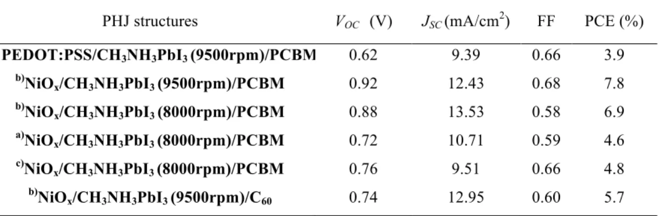
Table I. The photovoltaic parameters of CH
3NH
3PbI
3/PCBM hybrid solar cells.
PHJ structures V
OC(V) J
SC(mA/cm
2) FF PCE (%) PEDOT:PSS/CH
3NH
3PbI
3(9500rpm)/PCBM 0.62 9.39 0.66 3.9
b)
NiO
x/CH
3NH
3PbI
3(9500rpm)/PCBM 0.92 12.43 0.68 7.8
b)
NiO
x/CH
3NH
3PbI
3(8000rpm)/PCBM 0.88 13.53 0.58 6.9
a)
NiO
x/CH
3NH
3PbI
3(8000rpm)/PCBM 0.72 10.71 0.59 4.6
c)
NiO
x/CH
3NH
3PbI
3(8000rpm)/PCBM 0.76 9.51 0.66 4.8
b)
NiO
x/CH
3NH
3PbI
3(9500rpm)/C
600.74 12.95 0.60 5.7
Device configuration:
glass/ITO/NiO
xor PEDOT:PSS/CH
3NH
3PbI
3(8000 or 9500 rpm)/PCBM or C
60/BCP/Al
a)