Hydrogen plasma dry etching method for field emission application
T. C. Cheng, J. Shieh, W. J. Huang, M. C. Yang, M. H. Cheng, H. M. Lin, and M. N. Chang
Citation: Applied Physics Letters 88, 263118 (2006); doi: 10.1063/1.2218824 View online: http://dx.doi.org/10.1063/1.2218824
View Table of Contents: http://scitation.aip.org/content/aip/journal/apl/88/26?ver=pdfcov
Published by the AIP Publishing
Articles you may be interested in
Enhanced electron field emission from plasma-nitrogenated carbon nanotips
J. Appl. Phys. 111, 044317 (2012); 10.1063/1.3688252
Enhanced field emission from ZnO nanowires grown on a silicon nanoporous pillar array
J. Appl. Phys. 108, 114301 (2010); 10.1063/1.3516156
Field electron emission from individual diamond cone formed by plasma etching
Appl. Phys. Lett. 89, 063105 (2006); 10.1063/1.2266991
Field emission of silicon nanowires
Appl. Phys. Lett. 88, 213108 (2006); 10.1063/1.2206151
Fabrication of vertically aligned Si nanowires and their application in a gated field emission device
Appl. Phys. Lett. 88, 013112 (2006); 10.1063/1.2162692
This article is copyrighted as indicated in the article. Reuse of AIP content is subject to the terms at: http://scitation.aip.org/termsconditions. Downloaded to IP: 140.127.150.67 On: Wed, 10 Sep 2014 05:58:46
which is defined as the lowest energy required to remove an electron from the surface of a conducting material, to a point just beyond the metal’s surface, with zero kinetic energy. In other words, electrons having a low local work function will readily be emitted from the silicon nanowires to the vacuum level. Table I reveals that a lower hydrogen plasma etching time increased the local work function of the silicon nano-wires and led to their higher turn-on fields. In addition, the plot of ln共I/E2兲 vs 1/E, presented in Fig. 2共b兲, is a straight
line, indicating that the field emission from the SiNWs fol-lows Fowler-Nordheim behavior.16 Moreover, according to the FN method, the FN slope in our current case can be written as
FN plot =− 6.44⫻ 10
9⌽3/2
 . 共1兲
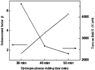
On the basis of Eq. 共1兲, the slope is related to the work function共⌽兲 and the field enhancement factor 共兲. The line intercepts on the vertical axis are also related to both the work function and the actual emission area of the active emitters. The field enhancement factor  may be used to demonstrate the degrees of field emission enhancement of tips of any shape on planar surfaces. Many researchers have demonstrated16–18 that the field enhancement factor  is an important parameter of the emission properties; it depends on the geometry of the nanowires, their crystal structure, and the distance between the emitter and anode. In this study, we found that the actual field enhancement factors, summarized in Table I, could be easily obtained from the FN plot when using the work function measured by Kelvin probe micros-copy. Our results indicate that the enhancement factor 共兲 increased upon increasing the etching time. Furthermore, electron emission occurred as a result of a combination of electrical and geometric contributions, but these individual effects cannot be separated readily. Although it is difficult from our experiments to identify the exact distribution of the emitting tips and the actual local fields on the emitting tips, the silicon nanowires in this letter provide some qualitative information regarding the field emission enhancement. Ac-cording to the simulations of Edgcombe and Valdré,19 the value of  is proportional to 共2.5+h/r兲0.9, where h is the length and r is the diameter of the emitting tip. In our pre-vious study,11 increasing the hydrogen plasma etching time sharpened the silicon nanowires and increased their lengths; thus, the field enhancement factor increased upon increasing the etching time. Moreover, Fig. 3 displays the observed variations in the field enhancement factors and the turn-on fields of the silicon nanowire emitters with respect to the etching time. In view of the field emission performance, it is interesting to note that the silicon nanowires that were sub-jected to the longest hydrogen plasma etching time共50 min兲 has the lowest turn-on field and the highest field enhance-ment factor. These results indicate that longer etching times will improve the field emission properties of samples used in many microelectronics applications.
In conclusion, the highly uniform 共diameter and distri-bution兲, well-aligned nanowire arrays can be readily pre-pared over large areas through hydrogen plasma dry etching alone, i.e., in the absence of a mask or catalyst. We measured the field emission properties of the different silicon nano-wires directly using a sharp anode in the SEM. Following the
FN model, we found that the hydrogen plasma etching time affects the geometry of the silicon nanowires and that it may be exploited to improve their field emission properties sub-stantially. In this letter, we provide a simple method for fab-ricating large-area, uniformly distributed nanowire emitters that can be used widely in many field emission applications, especially in field emission displays.
The authors would like to thank Professor C. S. Wu of the Mechanical Engineering Department, National Chiao-Tung University and Dr. Y. R. Chen of the Institute of Chem-istry, Academia Sinica for considerable support and technical assistance.
1Z. L. Wang, R. P. Gao, Z. W. Pan, and Z. R. Dai, Adv. Eng. Mater. 3, 657 共2001兲.
2C. X. Xu and X. W. Sun, Appl. Phys. Lett. 83, 3806共2003兲.
3J. Niu, J. Sha, X. Ma, J. Xu, and D. Yang, Chem. Phys. Lett. 367, 528 共2003兲.
4L. Gangloff, E. Minoux, K. B. K. Teo, P. Vincent, V. T. Semet, V. T. Binh, M. H. Yang, I. Y. Y. Bu, R. G. Lacerda, G. Pirio, J. P. Schnell, D. Pribat, D. G. Hasko, G. A. J. Amaratunga, W. I. Milne, and P. Legagneux, Nano Lett. 4, 1575共2004兲.
5L. Dvorson, G. Sha, I. Kymissis, C.-Y. Hong, and A. I. Akinwande, IEEE Trans. Electron Devices 50, 2548共2003兲.
6S. Itoh, M. Tanaka, and T. Tonegawa, J. Vac. Sci. Technol. B 22, 1362 共2004兲.
7Y. Cui and C. M. Lieber, Science 291, 851共2001兲. 8A. M. Morales and C. M. Lieber, Science 279, 208共1998兲.
9H. F. Yan, Y. J. Xing, Q. L. Hang, D. P. Yu, Y. P. Wang, J. Xu, Z. H. Xi, and S. Q. Feng, Chem. Phys. Lett. 323, 224共2000兲.
10S. T. Lee, Y. F. Zhang, N. Wang, Y. H. Tang, I. Bello, C. S. Lee, and Y. W. Chung, Mater. Res. 14, 1842共1999兲.
11M. C. Yang, J. Shieh, C. C. Hsu, and T. C. Cheng, Electrochem. Solid-State Lett. 8, C131共2005兲.
12H. Hoppe, T. Glatzel, M. Niggemann, A. Hinsch, M. Ch. Lux-Steiner, and N. S. Sariciftci, Nano Lett. 5, 269共2005兲.
13R. H. Fowler and L. Nordheim, Proc. R. Soc. London 119, 137共1928兲. 14S. Sadewasser, Th. Glatzel, M. Rusu, A. Jager-Waldau, and M. Ch.
Lux-Steiner, Appl. Phys. Lett. 80, 2979共2002兲. 15C. Tang and Y. Bando, Appl. Phys. Lett. 83, 659共2003兲.
16J. M. Bonard, K. A. Dean, B. F. Coll, and C. Klinke, Phys. Rev. Lett. 89, 197602共2002兲.
17M. C. Rossi, S. Salvatori, P. Ascarelli, E. Cappelli, and S. Orlando, Dia-mond Relat. Mater. 11, 819共2002兲.
18F. C. K. Au, K. W. Wong, Y. H. Tang, Y. F. Zhang, I. Bello, and S. T. Lee, Appl. Phys. Lett. 75, 1700共1999兲.
19C. J. Edgcombe and U. Valdré, Philos. Mag. B 82, 987共2002兲. FIG. 3. Field enhancement factors and turn-on fields of silicon nanowires obtained after different hydrogen plasma etching times.
263118-3 Cheng et al. Appl. Phys. Lett. 88, 263118共2006兲
This article is copyrighted as indicated in the article. Reuse of AIP content is subject to the terms at: http://scitation.aip.org/termsconditions. Downloaded to IP: 140.127.150.67 On: Wed, 10 Sep 2014 05:58:46