Fabrication and Characterization of Schottky Junctions
of Aluminum with Polyaniline Containing Hydrolysis Products
Wei-Chih Chen, Ten-Chin Wen,
*
,zand A. GopalanaDepartment of Chemical Engineering, National Cheng Kung University, Tainan 701, Taiwan
Schottky diodes based on Al/polyaniline共PANI兲, electrodeposited by cyclic voltammetry 共CV兲 with two different upper oxidation potentials, 0.8 and 1.1 V, respectively, were fabricated. Auger electron spectroscopy共AES兲 confirms the presence of hydrolysis products of PANI, benzoquinone共BQ兲/hydroquinone 共HQ兲 for PANI film deposited with a switch potential of 1.1 V. The electrical properties of the Al/PANI共with inbuilt hydrolysis products兲 and Al/PANI 共without hydrolysis products兲 junctions were evaluated at different temperatures by current-voltage characteristics and impedance spectroscopy measurements. The presence of inbuilt hydrolysis products with PANI influences the electrical properties of the junction. The junctions were found to be rectifying in both cases but with wide differences in junction parameters, such as barrier height, ideality factor, and saturation current density, between them. The temperature dependence of the impedance spectra of the devices was found to have variations. Impedance parameters of the devices were deduced from a proposed equivalent circuit. The combined analyses of current-voltage character-istics and impedance measurements reveal that the presence of hydrolysis products with PANI in Al/PANI junction increases the contact resistance, depletion layer thickness, and barrier height of the device.
© 2004 The Electrochemical Society. 关DOI: 10.1149/1.1795255兴 All rights reserved.
Manuscript submitted March 3, 2003; revised manuscript received April 14, 2004. Available electronically September 21, 2004.
Semiconducting conjugated polymers can be easily synthesized and obtained in the form of thin films suitable for device fabrication. Various conducting polymers such as polypyrrole, polythiophene, poly共3,4-ethylenedioxythiophene兲, and semiconducting polyaniline 共PANI兲 are used in molecular electronic devices.1-4The striking fea-ture of PANI is that its electronic properties can be altered by chemi-cal modifications, which provide significant effects on its physichemi-cal properties. This feature coupled with a high degree of chemical sta-bility in air makes PANI very attractive for a wide range of potential applications. Fabrication of solid-state heterojunction/Schottky de-vices is one of the most important applications for PANI.
Schottky devices have been successfully fabricated with metal and semiconducting polymers5-8and the electronic properties con-trolling the device performance, such as rectifying ratio, barrier height, and work function, have been evaluated through measure-ments of dark current density against applied voltage. Generally, metals possessing a high work function, such as Au, give ohmic contacts, while metals possessing a low work function, such as Al, provide rectifying contacts. The barrier generated at the metal/ polymer interface creates an environment for blocking charge carri-ers. The efficiency of the device is predominately determined by the injection efficiency of the minority carriers surmounting the barrier. Hence, the physical and chemical states of the polymer, which is used for establishing contact, are the determining factors that influ-ence the efficiency of the device.
A few interesting studies have been directed on the possible chemical interaction between metal and polymer at the interface.4,9 The dopants present in the conjugated polymer contribute to the chemical interaction with metal and result in an insulating layer on the metal surface. The electrical properties of metal contacts with doped polypyrrole,9 with polymeric anions, and doped poly关3-共4-octylphenyl兲-2,2⬘-bithiophene兴10with PF6⫺were analyzed in terms of insulating film formation. Also, chemistry-induced de-fects formed when metal atoms are deposited on the conjugated polymer surface are known to alter electronic properties of the devices.11,12Dannetun et al.13 have reported that aluminum atoms evaporated on the surface of poly共3-octylthiophene兲 films react with active groups in polymer chains to result in a complex. In a similar way, Lachkar et al.14reported sulfide-like complex formation at the
interface with metals like Cu and Ag as a result of interactions between the semiconducting conjugated poly共3-hexylthiophene兲 and the metal.
Hence, it becomes imperative to note that chemistry-induced de-fects formed at the interface between a semiconducting conjugated polymer and a metal can play a crucial role in deciding junction properties. For instance, a peculiar symmetrical but nonohmic be-havior has been noticed in the sandwich device, Al/doped poly 共3,4-ethylenedioxythiophene兲/indium-tin-oxide 共ITO兲.4However, the re-search has not been extended for any of such device with PANI as the semiconducuting polymer. This might be due to the absence of any complex forming groups in PANI with the contact metal.
Recently, our reports demonstrated that in situ induced hydroly-sis products of PANI, the BQ/HQ redox pair, significantly alter the impedance characteristics of PANI embedded with BQ/HQ.15-17 It would be interesting to evaluate the junction properties of the elec-tronic device fabricated with PANI having the induced hydrolysis products in it.
In the present study, we report the electrical features of junctions between a metal and electrochemically polymerized PANI in the doped form with incorporated BQ/HQ inbuilt in the PANI matrix. The influence of BQ/HQ on the Schottky barrier developed with Al and PANI共BQ/HQ兲 was further investigated. The Schottky diodes were fabricated by using Au whose work function is 4.8 eV higher than that of PANI共which lies between 4.1 and 4.28 eV18兲 to form an ohmic contact with PANI, while on the other side, aluminum pos-sessing a low work function of 3.7 eV was used to make a rectifying contact with PANI. The measurements of current-voltage and ac impedance were conducted to bring out the influence of in situ gen-erated hydrolysis products on junction properties of Schottky di-odes. PANI films were electrodeposited in different conductions by cyclic voltammetry and used for this purpose.
Experimental
Chemicals.—Reagent grade aniline 共Merck兲 was doubly dis-tilled, and the resulting colorless liquid was kept under nitrogen in the dark at 5°C. All other reagents were Merck or GR samples and used without pretreatment.
Electrodeposition of PANI with or without hydrolysis products.— Electrochemical deposition of PANI was made by using the Autolab PGSTAT 30 共Eco. Chemie B.V., The Netherlands兲 with a general purpose electrochemical system software. A three-electrode cell as-sembly was utilized with an Ag/AgCl reference electrode 共Ar-genthal, 3 M KCl, 207 mV vs. SHE at 25°C兲. Platinum wire was used as the counter electrode. A gold foil of area 1 cm2was used as the working electrode. A Luggin capillary, whose tip was set at a *Electrochemical Society Active Member.
aPresent address: Department of Industrial Chemistry, Alagappa University,
Karaikudi, India.
Auger electron spectroscopy.—Auger electron spectroscopy 共AES兲 measurements of PANI films were performed with ESCA 210 and MICROLAB 310D 共VG Scientific Ltd., UK兲 spectrometers. AES depth profiling was conducted at emission currents of 0.1 and 8 mA with gun tensions of 10 共electrons兲 and 3 kV 共ions兲, respectively.
Schottky diodes with PANI.—Approximately 100 nm thick strips of aluminum were vacuum evaporated at a pressure of⬃10⫺5 Torr to have metal contact with PANI. The active area of the metal/ polymer contact was 0.28 cm2. The fabricated devices of Au/PANI-a/Al and Au/PANI-b/Al are denoted as device a and device b, re-spectively. Such a sandwich structure was used for current-voltage and ac impedance measurements.
Current-voltage and ac impedance measurements.—Current-voltage characteristics were measured using model 2400 series SourceMeter共Keithley, USA兲 and scanned in the potential range between⫺1.3 and ⫹1.3 V. The impedance spectrum analyzer, IM6 共ZAHNER, Germany兲, with Thales software was employed to mea-sure and analyze the ac impedance spectra. The potential amplitude of ac was kept as 10 mV and its frequency range was used from 1 MHz to 500 Hz. AC impedance measurements were made at differ-ent applied dc voltages.
Results and Discussion
Preparation of PANI film with builtin hydrolysis products.— Electrodeposition of PANI was performed by cyclic voltammetry 共CV兲 at two different switching upper potentials, 0.8 and 1.1 V, respectively, to make PANI films, PANI-a and PANI-b, without and with hydrolysis products. CVs共Fig. 1兲 recorded with concomitant deposition of PANI with these two conditions clearly reveal the presence of BQ in PANI-b film deposited with the upper potential of 1.1 V. It is expected that electrodeposition of PANI by cyclic volta-mmetry with a switching potential⬎ 0.8 V, could result in BQ as the hydrolysis product.19-22 In Fig. 1b, besides the characteristic peak at 0.25 V for the conversion of leucoemeraldine to emeraldine 共polaronic radical cation兲 form of PANI, a peak at 0.60 V for the oxidation of head-to-tail dimer, and the peak at 0.80 V for the gen-eration of diradical dications in the PANI structure, the presence of a peak at 0.50 V indicates the formation of a degradation product of PANI, BQ. Kobayashi et al.19and Stilwell and Park20assigned the peak around 0.50 V during PANI growth for the generation of BQ. Several other researchers have also reported the formation of BQ as the hydrolysis product during PANI deposition.23,24Consecutive re-actions involving the hydrolysis of the quinoid site of PANI 共emer-aldine form兲 and the formation of a p-aminophenol type intermedi-ate via an electrochemical electron transfer followed by a chemical reaction25result in BQ. Reduced PANI with a shorter chain length can be a result of this process.
In contrast to Fig. 1b, the peak representing BQ formation was not obvious when PANI-a was deposited with the upper potential limit of 0.80 V共Fig. 1a兲, informing a negligible proportion of BQ generation during deposition of PANI-a.
Our aim is to study and compare the electronic and junction properties of these two PANI films with Al as the contact metal. Hence, film thicknesses of these two films were controlled so as to be close to each other. The thickness共d兲 of the deposited PANI films was estimated from the charge necessary to convert the leucoemer-aldine form of PANI to the emerleucoemer-aldine form共using the area under the first redox process in the voltammograms兲.26,27The following equation was used to calculate the thickness of films
d⫽ Q Mw
zFA 关1兴
where Q is the charge under the first cyclic voltammetric peak; Mw the molecular weight of aniline共93.13 g mol⫺1兲; z ⫽ 0.5 共number of electrons/aniline unit兲; A the area of the electrode 共1.0 cm2兲; the specific density of aniline共1.02 g cm⫺3兲, and F is the Faraday con-Figure 1. CVs of growth of PANI films on gold electrodes with the upper
stant. The thickness of films were estimated as 1.7 and 1.8m for PANI-a and PANI-b, respectively. Thus, the two films deposited at the two different conditions were controlled so as to have a similar thickness.
Auger profile of oxygen concentration in PANI films.—The inclu-sion of BQ in PANI-b was confirmed by Auger electron spectros-copy共AES兲. Spectra of PANI-a and PANI-b were recorded to ascer-tain the presence of builtin BQ in the bulk of polymer films. The depth profiles of the O signal were compared共Fig. 2兲 and found that PANI-b has a higher proportion of BQ in the film. Previously, X-ray photoelectron spectroscopy 共XPS兲 was used to obtain such information.15,16The Auger profile of PANI-b clearly shows the ex-istence of BQ in the film. The observed higher concentration of O at the surface is probably due to the migration of BQ from the bulk of the polymer to the surface during the film drying process.
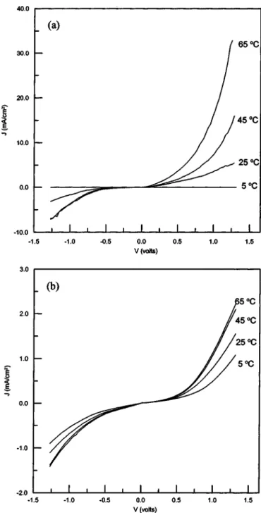
Electronic properties of the Schottky barrier.—Schottky barrier devices were fabricated independently with these two PANI films in the sandwich configuration, Au/PANI-a/Al共device a兲 and Au/PANI-b/Al共device b兲. Figure 3 shows typical current density vs. voltage (J-V) characteristics of these devices at various temperatures. The J-V relation for both devices is asymmetrical and rectifying. Strik-ing differences in the J-V characteristics between the two devices were observed, and these are attributed to the presence of BQ in PANI film. The J-V curves for different temperatures of device b are close to each other and have low current densities共less than 2.5 mA/cm2兲. In contrast, device a shows temperature dependent J-V curves. This indicates that the carrier transport in metal/ semiconductor contacts are different between these devices.
The transport of charge from the semiconductor over the poten-tial barrier into the metal could be described by the thermionic emis-sion theory or the diffuemis-sion theory of metal/semiconductor rectification.28
The current density共Fig. 3兲 could be explained by using Rich-ardson’s equation expressed as
J⫽ JSexp
冉
qVnkT
冊
关2兴where JSis the saturation current density, V the applied potential, q the electronic charge, n the ideality factor, k the Boltzmann constant, and T is the absolute temperature. The saturation current density is defined as
JS⫽ A*T2
exp
冉
⫺qBkT
冊
关3兴where A*is the Richardson constant共⫽120 A K⫺2cm⫺2for a free electron兲, and Bis the barrier height at the metal/semiconductor interface.
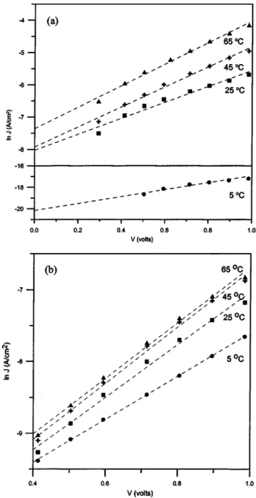
The ln J vs. V plots of device a and b at different temperatures are given in Fig. 4a and b, respectively. The values of JSand n were calculated for different temperatures from the intercept and slope of the linear region of ln J vs. V plots, and are listed in Table I. Fur-thermore, the values of barrier height共obtained according to Eq. 3兲 and rectification ratio共at ⫾0.7 V兲 are also presented in Table I.
Large values of the ideality factor of device a共⬃10-15兲 and b 共⬃8-14兲 were obtained 共Table I兲, and these results are in agreement with that of polypyrrole/metal Schottky device3for which the ideal-ity factor was reported as 10. The higher values of n noticed for the conducting polymers are due to the fact that these polymers are present in the form of aggregates of primary and secondary par-Figure 2. The Auger depth profiles of O element from共a兲 PANI-a and 共b兲
PANI-b films.
Figure 3. Temperature dependence of current density vs. applied voltage
(J-V) rectification characteristics for共a兲 a/Al and 共b兲 Au/PANI-b/Al devices.
ticles, irrespective of polymerization conditions. Accordingly, two different electron transport mechanisms are feasible.29Additionally,
mer as a result of the chemical reaction. The formation of an insulating film is supposed to occur via the reaction of the oxygen groups in the dopant/polymer with metal. The dioxoethylene bridge present in poly共3,4-ethylenedioxythiophene兲 共PEDOT兲 interacts with aluminum to result in an insulating layer.4As a consequence of the insulating layer, bands of conducting polymers are expected to be affected. Also, the interfacial layer can induce reorientations of the molecular backbones.31In the present study, the coexistence of BQ with PANI in device b may hasten interaction with Al and the subsequent changes in interfacial characteristics can be inferred from ac impedance studies on the interface.
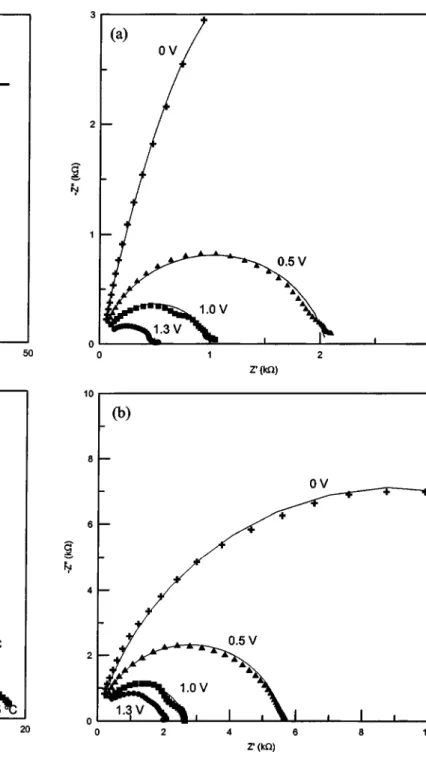
AC impedance analyses.—To get more insight into the interfacial characteristics at Al/PANI junction, ac impedance measurements of device a and b were independently performed as functions of tem-perature and bias voltages. Figure 5 and 6 display the impedance behavior of device a and b at different temperatures and bias volt-ages, respectively. It is indicated from Fig. 5 and 6 that there are differences in the impedance behavior between these two devices. The temperature response of impedance共Fig. 5兲 for these devices is similar to J-V characteristics共Fig. 2兲. Device b shows a lower tem-perature dependence on impedance than device a. This indicates that the observed differences in J-V characteristics and impedance may have the same origin. The reason for such differences is analyzed in terms of the presence of BQ in device b in contrast to device a. The impedance parameters are deduced from a proposed equivalent cir-cuit共Fig. 5a, insert兲.
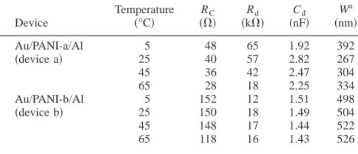
Figure 5 and 6 reveal that the impedance response with temperature/bias voltage is a single semicircle. The response can be represented by an equivalent circuit with one parallel RC circuit (Rd and Cd) in series with the contact resistance (RC)10as shown in the inset of Fig. 5a. The elements of Rdand Cdin this model represent the resistance and the capacitance of the depletion layer. Best-fit curves to the equivalent circuit are represented as solid lines in Fig. 5 and 6. The derived best fit values of the corresponding element parameters are presented in Table II. Two striking differences can be noticed in the impedance parameters of device b in contrast to de-vice a. Dede-vice b has higher RCand thickness of the depletion layer in comparison to device a, suggesting a build up of an insulating material along with PANI in the case of device b.
Figure 4. Temperature dependence of ln J vs. V characteristics of the
junc-tions for共a兲 Au/PANI-a/Al and 共b兲 Au/PANI-b/Al devices.
Table I. Electronic parameters of Schottky junctions for the devices.
Device
Temperature
共°C兲 Saturation current densityJS共A/cm
2兲 Ideality factor n Barrier height B共V兲 Rectification ratio r共at 0.7 V兲
Au/PANI-a/Al共device a兲 5 1.77 ⫻ 10⫺9 12.53 0.81 72.44
25 3.29 ⫻ 10⫺4 14.76 0.62 20.89 45 3.63 ⫻ 10⫺4 11.77 0.66 18.62 65 6.36 ⫻ 10⫺4 10.31 0.69 57.54 Au/PANI-b/Al共device b兲 5 2.49 ⫻ 10⫺5 13.91 0.64 0.85 25 2.25 ⫻ 10⫺5 10.64 0.69 0.91 45 2.37 ⫻ 10⫺5 9.31 0.74 0.95 65 2.62 ⫻ 10⫺5 8.87 0.79 1.23
Now, it is important to compare the value of RCbetween the two diodes. At any given temperature, the RCvalue of device b is around 100⍀ higher than that of device a. This result provides clear evi-dence for the presence of resistive BQ at the Al/PANI-b interface to increase the resistance of simple PANI by a value of 100⍀.
However, it is worthwhile noting the different behavior of BQ, a molecular material, in comparison to the previous reports of forming a thin insulating film at the metal/polymer interface in the presence of larger size polymeric dopant, polystyrenesulfonate共PSS兲.4In the case of PEDOT doped with PSS, two clear partially overlapping semicircles have been noticed.4The high frequency, bias voltage independent semicircle was attributed to the formation of a thin insulating layer at the metal/PEDOT interface as a result of interac-tion between sulfonate groups and aluminum atoms. The device
structure was interpreted as a metal-insulator-semiconductor junc-tion. The low frequency, bias voltage dependent semicircle has been assigned to the occurrence of a depletion layer. In the present study, a single semicircular impedance behavior was noticed共Fig. 5 and 6兲 for the metal/PANI-b interface, even in the definite presence of BQ. Hence, the presence of BQ is expected to increase the resistance at the junction by its mere presence at the interface blocking the elec-trode surface to be in contact with the semiconducting polymer. The reason for the absence of double semicircles in the present study could be determined by exploring more about the parameters related to the depletion layer.
A decreasing trend in the resistance of the depletion region (Rd) with the increase in temperature can be seen from the impedance spectra共Fig. 5兲. The values of Cdderived from simulation can be Figure 5. Temperature dependence on Nyquist diagrams for共a兲
Au/PANI-a/Al and共b兲 Au/PANI-b/Al devices at the applied bias potential of 0 V. Inset in共a兲 is the corresponding equivalent circuit.
Figure 6. Nyquist diagrams for共a兲 Au/PANI-a/Al and 共b兲 Au/PANI-b/Al
used to calculate the depletion width共W兲 according to Eq. 4 Cd⫽
0A
W 关4兴
where0is the permittivity of free space and 共assumed to have a value of 3兲10is the relative permittivity of the polymer. The deple-tion layer for device b is thicker共⬃500 nm兲 than device a 共⬃300 nm兲 共Table II兲. This can suppress the probability of charge transport through tunneling for device b.7The observed higherBfor device b is consistent with this observation. Otherwise, device a has a thin-ner depletion width than device b, which arises from the fact that the depletion width is inversely proportional to the conductivity. The increased thickness of the depletion layer can arise from the follow-ing reason. When PANI is hydrolyzed to result in BQ, shorter chains of PANI in its reduced form could be formed.17The coexistence of BQ and reduced PANI with a shorter chain length, makes the matrix more resistive and causes the increased depletion layer. The clear absence of double semicircles in the impedance measurements of our studies is manifested from the comparatively greater thickness of the depletion layer.
Figure 6 shows the impedance characteristics recorded at several applied bias potentials. The values of related parameters obtained from simulation of the equivalent circuit共Fig. 5a兲 are listed in Table III. The impedance responses共Fig. 6兲 of both devices strongly
de-fested from the increased resistance arising from the coexistence of BQ/HQ and reduced PANI with shorter chain lengths at the Al/PANI interface.
Acknowledgments
The authors are grateful to the National Science Council in Tai-wan for its financial support through NSC 91-2214-E-006-028 and NSC 92-2214-E-006-003.
National Cheng Kung University assisted in meeting the publication costs of this article.
References
1. V. C. Nguyen and K. Potje-Kamloth, Thin Solid Films, 338, 142共1999兲. 2. D. M. de Leeuw and E. J. Lous, Synth. Met., 65, 45共1994兲.
3. R. Gupta, S. C. K. Misra, B. D. Malhotra, N. N. Beladakere, and S. Chandra, Appl.
Phys. Lett., 58, 51共1991兲.
4. W. Bantikassegn and O. Ingana¨s, Thin Solid Films, 293, 138共1997兲. 5. K. Kaneto and W. Takashima, Curr. Appl. Phys., 1, 355共2001兲.
6. S. C. K. Misra, M. K. Ram, S. S. Pandey, B. D. Malhotra, and S. Chandra, Appl.
Phys. Lett., 61, 1219共1992兲.
7. R. Singh and A. K. Narula, Appl. Phys. Lett., 71, 2845共1997兲. 8. C. H. Yang, J. Electrochem. Soc., 146, 1939共1999兲. 9. W. Bantikassegn and O. Ingana¨s, J. Phys. D, 29, 2971共1996兲. 10. W. Bantikassegn and O. Ingana¨s, Synth. Met., 87, 5共1997兲.
11. W. Bantikassegn, P. Dannetun, O. Ingana¨s, and W. R. Salaneck, Thin Solid Films, 224, 232共1993兲.
12. P. Dannetun, M. Lo¨gdlund, M. Fahlman, M. Boman, S. Stafstro¨m, and W. R. Salaneck, Synth. Met., 55-57, 212共1993兲.
13. P. Dannetun, M. Boman, S. Stafstro¨m, and W. R. Salaneck, J. Chem. Phys., 99, 664
共1993兲.
14. A. Lachkar, A. Selmani, E. Sacher, M. Leclerc, and R. Mokhliss, Synth. Met., 66, 209共1994兲.
15. W. C. Chen, T. C. Wen, C. C. Hu, and A. Gopalan, Electrochim. Acta, 47, 1305
共2002兲.
16. W. C. Chen, T. C. Wen, and A. Gopalan, Electrochim. Acta, 47, 4195共2002兲. 17. W. C. Chen, T. C. Wen, and A. Gopalan, Synth. Met., 128, 179共2002兲. 18. S. S. Pandey, S. C. K. Misra, B. D. Malhotra, and S. Chandra, J. Appl. Polym. Sci.,
44, 911共1992兲.
19. T. Kobayashi, H. Yoneyama, and H. Tamura, J. Electroanal. Chem., 161, 419
共1984兲.
20. D. E. Stilwell and S. M. Park, J. Electrochem. Soc., 135, 2254共1988兲. 21. D. E. Stilwell and S. M. Park, J. Electrochem. Soc., 135, 2491共1988兲. 22. D. E. Stilwell and S. M. Park, J. Electrochem. Soc., 135, 2497共1988兲. 23. R. L. Hand and R. F. Nelson, J. Am. Chem. Soc., 125, 1059共1978兲. 24. D. E. Stilwell and S. M. Park, J. Electrochem. Soc., 136, 427共1989兲. 25. Y. B. Shim, M. S. Won, and S. M. Park, J. Electrochem. Soc., 137, 538共1990兲. 26. Lj. Duic and S. Grigic, Electrochim. Acta, 46, 2795共2001兲.
27. Z. Mandic and Lj. Duic, J. Electroanal. Chem., 403, 133共1996兲.
28. S. M. Sze, Physics of Semiconductor Devices, p. 245, Wiley, New York共1993兲. 29. S. Angappane, N. Rajeev Kini, T. S. Natarajan, G. Rangarajan, and B. Wessling,
Thin Solid Films, 417, 202共2002兲.
30. A. Bozkurt, C. Ercelebi, and L. Toppare, Synth. Met., 87, 219共1997兲.
31. R. Lazzaroni, J. L. Bre´das, P. Dannetun, C. Fredriksson, S. Stafstro¨m, and W. R. Salaneck, Electrochim. Acta, 39, 235共1994兲.
W is calculated from Eq. 4.
Table III. The best fitting values of the equivalent circuit ele-ments from the simulation of impedance data for two devices at different applied bias potentials.
Device Applied potentials 共V兲 共⍀兲RC 共k⍀兲Rd 共nF兲Cd W a 共nm兲 Au/PANI-a/Al 共device a兲 00.5 4053 572.1 2.822.89 267260 1.0 55 1.1 3.51 215 1.3 50 0.5 3.83 198 Au/PANI-b/Al 共device b兲 00.5 150131 185.6 1.491.44 504522 1.0 169 2.6 1.39 541 1.3 126 2 1.39 541 a