國立臺灣大學理學院物理學系 碩士論文
Department of Physics College of Science
National Taiwan University Master Thesis
高敏感度光偵測器之製程與研究 Highly Sensitive Photodetector Based on
n-ZnO/p-Si-nanotips Heterostructure
朱峯慶
Feng-Ching Chu
指導教授: 陳永芳 博士 Advisor: Yang-Fang Chen, Ph.D.
中華民國 98 年 7 月
July, 2009
誌謝
在台大的日子一轉眼過了二年,碩士班的生活即將結束。一路走來受到許多 貴人的相助,在這短短一頁文字中實在難以道盡,僅以此獻上峯慶由衷的感激與 祝福。
首先感謝我的指導老師─陳永芳教授。無論是學業上、做人處事或是面對事 情的態度,老師都做了最好的典範。即使老師在學術界已有如此崇高的地位,仍 不斷的閱讀國外期刊,來吸取新的知識。這讓我瞭解面對各種挑戰或際遇時,都 應秉著積極的心態、謙虛的態度,並不斷的學習新的知識。亦感謝口試委員林泰 源與沈志霖教授抽空前來給予學生指導與建議。另外感謝張顏暉與梁啟德教授在 報告中的建議與指導,讓我受益良多且備感榮幸。
感謝實驗室裡所有學長的幫忙,仲良、俊儀、群雄、志偉、志銘學長等,你 們的指導、建議和鼓勵讓我在實驗中更有信心。也感謝一起在半導體實驗室中打 拼的同學:曉聖、宇倫、鴻齊、人毅等。祝福大家以後無論是工作或課業都順利。
感謝我的好朋友們,百謙、中承,謝謝你們讓我在碩士班的生活中,增添了 不少樂趣,此外更要感謝常常熬夜陪我做實驗的毓芬,妳給我的鼓勵是我前進最 大的理由,由衷的感謝妳,在生活及課業上不斷的督促我,謝謝妳。
最後我要感謝我的家人,長久以來對我的栽培和支持,是我不斷前進的動力。
謝謝我的父親朱正雄先生與母親林鳳娥女士,還有我的大姐家慧與二姐家敏,謝 謝父母從小對我們的栽培與教誨。我也要感謝我的爺爺朱秋冬先生與奶奶黃來有 女士,雖然您們無法看到我從研究所畢業,但是我由衷的感謝您們,並把這畢業 的快樂與榮耀跟您們分享。
最後,謝謝每位關心我的朋友,謝謝大家。
摘要
本文中我們首次設計研製與探測氧化鋅(ZnO)和矽奈米尖錐(Si-nanotip)異 質接面的高效率光偵測二極體,首先將鍍有銀奈米顆粒當蝕刻光罩的 P 型矽晶圓 放入反應式離子蝕刻機(reactive ion etching,RIE)中進行蝕刻,然後製備出 P 型 矽 奈 米 尖 錐 結 構 (p-Si-nanotips) , 接 著 利 用 電 子 束 蒸 鍍 系 統 (e-beam evaporator),在 P 型矽奈米尖錐上沉積一層 N 型的氧化鋅薄膜。由我們的研究發 現,氧化鋅和矽奈米尖錐異質接面的光二極體與平面的矽(Si)和氧化鋅異質接面 光二極體一相比較下,氧化鋅和矽奈米尖錐異質接面的光偵測二極體有著更好的 光敏感度跟光響應度。
利用氧化鋅和矽奈米尖錐異質接面來增強光敏感度和光響應度的主要機制是 我們利用矽奈米尖錐結構來減少其反射率進而增加其吸收率,且一維的奈米尖錐 結構的表面積比平面結構的表面積還多,所以氧化鋅和矽奈米尖錐的接觸面積會 遠比氧化鋅和矽平板基板的接觸面積大很多。基於以上二個原因,所以我們增強 了氧化鋅和矽光偵測二極體的敏感度和響應度。
關鍵詞:
氧化鋅、光偵測器、矽奈米尖錐、電子束蒸鍍、光響應。
Abstract
ZnO/Si-nanotips heterostructure is introduced as a new and efficient photodiode for the first time. P-type Si-nanotips were fabricated by reactive ion etching (RIE) with the etching mask using Ag nanoparticles, and n-type was deposited by e-beam evaporation. It is found that n-ZnO/p-Si-nanotips diode possesses a highly sensitive photoresponse when comparing with its n-ZnO/p-Si-planar counterpart.
The underlying mechanism can be attributed to the enhanced absorption due to light trapping by Si nanotips array as well as the enhanced area of p-n junction due to the inherent nature of one-dimensional nanostructures.
Key Word:
ZnO, photodetector, Si-nanotips, e-beam evaporation, responsivity.
Contents
口試委員會審定書...I
誌謝 ... II
摘要 ... III
Abstract ...IV Contents... V List of Figures ... VII List of Tables ... XII
1. Introduction ... 1
2. Theorical Background ... 5
2.1 Properties of ZnO ... 6
2.1.1 Crystal Structure ... 6
2.1.2 ZnO Growth Methods... 7
2.1.3 Optical Transition in ZnO Material ... 7
2.1.4 Divices Based on ZnO... 7
2.2 Photodetector... 9
2.2.1 Mechanism and Calculation of Optical Absorption ... 9
2.2.2 Photoconductor... 12
2.2.3 Photodiode ... 13
2.3 Antireflection structure... 16
2.3.1 Introduction ... 16
2.3.2 Theory of Antireflection... 18
2.4 Photoluminescence (PL) Spectroscopy ... 21
2.4.1 Photoluminescence Emission ... 21
2.4.2 Recombination Processes ... 23
2.5 Raman Spectroscopy ... 25
2.5.1 Anti-Stokes and Stokes Lines... 27
3. Experimental Details... 32
3.1 Photoluminescence Apparatus... 33
3.2 Raman Scattering Apparatus ... 34
3.3 DC Sputter Deposition ... 38
3.4 Reactive Ion Etching ... 40
3.5 Evaporation... 41
3.6 Scanning Electron Microscopy... 43
4. Fabrication and characterization of Si-nanotips array ... 48
4.1 Introduction ... 49
4.2 Experiment ... 49
4.3 Results and Discussion ... 51
4.4 Summary... 60
5. Highly Sensitive Photodetector Based on n-ZnO/p-Si-nanotips Heterostructure... 62
5.1 Introduction ... 63
5.2 Experiment ... 64
5.3 Results and Discussion ... 67
5.4 Summary... 76
6. Conclusion... 79
List of Figures
Fig. 2.1 The crystal structures shared by ZnO (a) cubic rocksalt (b) cubic znic blend (c)
hexagonal wurtzite... 6
Fig. 2.2 Optical absorption process for (a) hν=Eg (b) hν>Eg (c) hν<Eg.... 10
Fig. 2.3 Optical absorption coefficients for many photodetector materials. ... 11
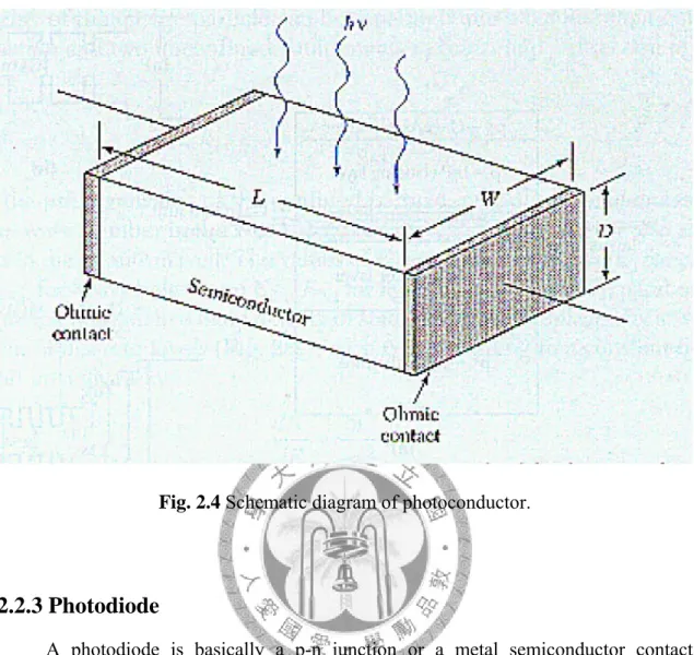
Fig. 2.4 Schematic diagram of photoconductor... 13
Fig. 2.5 (a) Band to band excitation of electron-hole pair (b) Internal photoemission of excited electron from metal to semiconductor... 15
Fig. 2.6 Schematic diagram of SWS. ... 17
Fig. 2.7 Geometry of the pillar array.. ... 18
Fig. 2.8 Effective mediums: (a) a multilevel surface profile the effective medium is a film stack (b) for a continuous surface profile the effective medium is a grandient-index film.. ... 20
Fig. 2.9 Graded refractive index model... 20
Fig. 2.10 (a) The lowest point of conduction band localizes at the same value of K as
the highest point of the valence band. The threshold frequency w for absorption phonon is given by the band gap. (b) The indirect transition involves both photon and phonon, because the band edges of the conduction bands and valence bands are separated in K space. The absorption threshold for the indirect transition is at Eg .. ... 23
Fig. 2.11 Illustration of different processes to make light emission in semiconductors.
………..24
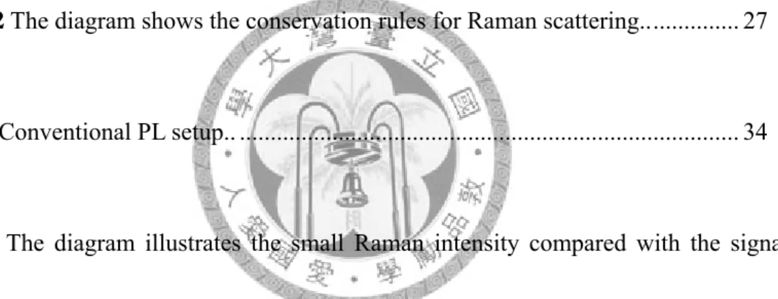
Fig. 2.12 The diagram shows the conservation rules for Raman scattering... 27
Fig. 3.1 Conventional PL setup.. ... 34
Fig. 3.2 The diagram illustrates the small Raman intensity compared with the signal
from a strong PL emitter. It also shows that both PL and Raman data can be obtained with the same experimental arrangement.. ... 35
Fig. 3.3 The schema of a Raman microscope. The microscope objective lens focusesthe
laser beam to a spot size of about 1um. Scattered light is transmitted through thebeam splitter to the double monochormator, giving the Raman spectrum of the selected region.
Visible light from the illuminator is reflected from the sample to a video camera, giving a realtime image to the allow position of the probe beam. The sample can be moved on
Fig. 3.4 A schematic illustration of the apparatus of DC sputtering deposition... 39
Fig. 3.5 The RIE system of Plasmalab 80 Plus: (a) an overall view (b) a schematic of
reacting chamber with two parallel plates and a few hundred watts of RF electromagnetic field applied on it.. ... 41
Fig. 3.6 An overall view of (a) the thermal evaporation machine (b) the e-beam
evaporation machine... 43
Fig. 3.7 Summary of the range and spatial resolution of backscattered electrons,
secondary electrons, X-rays, and Auger electrons for electrons incident on a solid.. . 47
Fig. 4.1 Schematic diagram for the fabrication procedure... ... 50
Fig. 4.2 Scanning electron microscope images of Ag nanoparticles deposited on Si
wafer at different temperatures (a) 300 (b) 400 (c) 500 (d) 600 ...℃ ℃ ℃ ℃ ... 53
Fig. 4.3 Morphology of Si-nanotips array fabricated by RIE with different times
(a)10min (b) 20 min (c) 30 min (d) 40 min... ... 56
Fig 4.4 The grooves deep of Si nanotips array in different RIE times.... ... 57
Fig 4.5 Reflectivity for Si nanotips with different RIE times.... ... 58
Fig. 4.6 The average reflectivity for Si nanotips with different RIE time in visible light
region... 60
Fig. 5.1. Schematic plots showing the fabrication process and the device structure of
n-ZnO/p-Si-nanotips photodiode... 66
Fig. 5.2. (a) Scanning electron microscope image of Ag nanoparticles deposited on Si
wafer (b) Morphology of Si-nanotips array (c) ZnO films deposited on Si-nanotips (d) Detailed micrograph of ZnO films deposited on Si-nanotips... 68
Fig. 5.3. (a) Optical reflectance spectra of bulk Si (rectangular curve), Si-nanotips array
(triangle curve), n-ZnO/p-Si-nanotips (rhombus curve) structure and n-ZnO/p-Si-planar (circle curve) structure. (b) Raman spectrum of ZnO films deposited on p-Si nanotips (c) Optical transmittance of ZnO films deposited on glass (d) Photoluminescence of ZnO films deposited on p-Si-nanotips... ... 72
Fig. 5.4. (a) The current-voltage curves of n-ZnO/p-Si-planar (dashed curve) and
n-ZnO/p-Si-nanotips (solid curve) photodiodes measured in a dark room (insert:
current-voltage curve of Al contact on p-Si (left); current-voltage curve of Ti/Au contact on n-ZnO (right)) (b) Spectral photoresponsivities of n-ZnO/p-Si-planar (dashed curve) and n-ZnO/p-Si-nanotips (solid curve) photodiodes... ... 74
List of Tables
Table 4.1 Detailed list of Si nanotip groove deep………. 57
Table 4.2 Detailed list of Si nanotips reflectivity average in visible region…………..60
Chapter 1
Introduction
Chapter 1 Introduction
Owing to fiber-optic communication development, the highly sensitive optical detector is getting more and more important. It is aims to transmit information by sending optical signals through an optical fiber. Because of the advantages over electrical transmission, optical fibers have been widely used to replace copper wire in communications recently. Currently, fiber-optic communication has been used in many different applications. For example, it can be used in transmitting telephone signals, internet communication, and cable television signals. One of the most important parts of fiber-optic communication is a receiver, which converted optical signals into electronic signals. The main component of an optical receiver is a photodetector of semiconductor based photodiode. Several types of photodiodes have been developed, including p-n photodiodes,1-2 p-i-n photodiodes,3-4 and avalanche photodiodes.
Ultraviolet (UV) photodetectors have been widely used, including military and civilian areas,5 missile launching detection, flame sensing, UV radiation calibration and monitoring, chemical and biological analysis, optical communications, as well as astronomical studies. In these applications, high responsivity, high response speed, minimum noise, use low biasing voltage and current, and be reliable under operating condition are all common desirable characteristics. Based on the intensive studies of wide bandgap materials the responsivity and stability of UV photodetectors have
beengreatly improved. Among these possibilities, zinc oxide (ZnO) is one kind of material which is very attractive due to its strong UV photoresponse, well-established synthesis methods, and the capability of operating at high temperature and in harsh environments.
P-n photodiode is a high efficiency photodetector due to the high field depletion region, and it has a high response speed. Internal noise in the photodiodes is very low, providing a high signal-to-noise ratio. And the photodiode produces more linear photoresponse and higher sensitivity than the photoconductor.
In this work, we will introduce a new and efficient photodiode based on ZnO/Si-nanotips heterojunction. An enhanced responsivity has been successfully demonstrated. This thesis includes the detailed fabrication process for our newly designed photodetector. In addition, the characteristics of our developed ZnO/Si-nanotips heterojunction photodetector have been investigated. The underlying mechanism for the enhanced photoresponse has also been discussed.
References
1. H. Y. Kim, J. H. Kim, Y. J. Kim, K. H. Chae, C. N. Whang, J. H. Song, and S. Im, Optical materials, 17 141 (2001).
2. C. H. Park, I. S. Jeong, J. H. Kim, and Seongil lm, Appl. Phys. Lett. 82, 3973 (2003).
3. Yuriy Vygranenko, Kai Wang, and Arokia Nathan, Appl. Phys. Lett. 89, 172105 (2006).
4. Kai Wang, Yuriy Vygranenko, and Arokia Nathan, Thin Solid Films 515, 6981 (2007).
5. Lei Luo, Yanfeng Zhang, Samuel S. Mao, and Liwei Lin, Sensors and Actuators A
127, 201 (2006).
Chapter 2
Theoretical Background
Chapter 2 Theoretical Background
2.1 Properties of ZnO
2.1.1 Crystal Structures
Most of the group II-VI binary compound semiconductors have crystal structures of either cubic zinc-blende or hexagonal wurtzite structure where each anion is surrounded by four cations at the corners of a tetrahedron. This tetrahedral coordination is typical of sp3 covalent bonding, but these materials also have a substantial ionic character.
ZnO is a II-VI compound semiconductor whose ionicity resides at the borderline between covalent and ionic semiconductor. The crystal structures shared by ZnO are wurtzite, zinc blende , and rocksalt, as schematically shown in Fig. 2.1. At ambient conditions, the thermodynamically stable phase is wurtzite.1
Fig. 2.1 The crystal structures shared by ZnO (a) cubic rocksalt (b) cubic znic blend (c) hexagonal wurtzite.
2.1.2 ZnO Growth Method
The growth of ZnO thin films has been widely studied for acoustical and optical devices. The early reports the deposition method of ZnO utilizing growth techniques such as magnetron sputtering and chemical vapor deposition. However, the films were polycrystalline. In order to attain high quality, ZnO single crystal films are fabricated by rf magnetron sputtering, molecular-beam epitaxy (MBE), pulsed-laser deposition (PLD), metal organic chemical vapor deposition (MOCVD), hydride or halide vapor-phase epitaxy (HVPE), and e-beam evaporator techniques.1-2
In this thesis, we focused on the fabrication of deposited ZnO films on p-Si by using e-beam evaporation equipment.
2.1.3 Optical Transition in ZnO Material
Optical transitions in ZnO have been invested by many kinds of experimental techniques, such as optical absorption, transmission, reflection, photoreflection, spectroscopic ellipsometry, photoluminescence, cathodoluminescence, and calorimetric spectroscopy.
ZnO has attracted more and more attention due to its optical property of the large binding energy of the exciton (60 meV),1 over 80 % transmittance of visible light and the wide band gap (3.2 eV).3
2.1.4 Devices Based on ZnO
ZnO is a multifunctional material with good optical transmission, electrical
conductivity, and cathodoluminescence for electronic device such as light-emitting diodes,4-5 photodiodes,3 metal-insulator-semiconductor diodes and transparent thin film transistors. For example, Drapak6 introduced ZnO-based hetererostructure LED. He used p-Cu2O layer, which was obtained by thermal oxidation of a Cu metal layer deposited on ZnO substrates. The fabricated LED structures have been measured by electroluminescence (EL) in both forward and reverse biases, and a broad spectrum with maxima at 540 nm has been observed. Except the p-n junctions, ZnO EL properties have been investigated by fabricating metal insulator semiconductor (MIS) structures7 which do not require p-type ZnO.
In this work, we investigated the optical and electrical characteristics of ZnO based photodiodes. There have been many reports regarding the photoresponse properties of the ZnO-based photodetector. Jeong et al.8 have investigated the photoelectric properties of n-ZnO/p-Si photodiode (PD), which detect visible photons in the depleted p-Si and simultaneously detect UV photons in the depleted n-ZnO by employing two related photoelectric mechanisms. The p-Si/n-ZnO diodes exhibited high photoresponsivities of 0.5 and 0.3 AW-1 for UV and red photons, respectively.
2.2 Photodetector
Photodectors are semiconductor devices can detect optical signals through electronic processes. The operation of a general photodetector based on three processes:
(1) electron-hole pairs generation by a incident light, (2) carrier transport and/or multiplication by whatever current gain mechanism if present, and (3) extraction of carriers as terminal current to provide the output signal.9
Recently, photodetector plays an important role in optical-fiber communication systems. They established a process converting optical signals into electrical signals.
For such applications, the photodetectors must satisfy high sensitivity at operating wavelength, high response speed, and low noise. It also should have compacted size, use low biasing voltage and current, and be reliable under the required operating
conditions.
2.2.1 Mechanism and Calculation of Optical Absorption
Since the photoelectric effect is based on the incident light with energy hν, the wavelength is related to energy transition E, with simple but important relationship
) 12400 (
eV E hc E
(2.1)where λ is the wavelength of incident light, c is the speed of light, h is the Planck’s constant, △E is the transition of energy levels. Fig. 2.2 shows the basic transition in a semiconductor.10
) (
Fig. 2.2 Optical absorption process for (a) hν=Eg (b) hν>Eg (c) hν<Eg.
When the semiconductor is illuminated by the photon with energy larger than the band gap energy or equal to the band gap, an electron-hole pair is generated and, in addition, the excess energy (hν-Eg) is dissipated as heat, as shown in Fig. 2.2 (a) and Fig. 2.2 (b). Both processes are called intrinsic transitions. Besides, energy less than Eg, a photon will be absorbed by the available energy states in the forbidden band gap, which is generated by chemical impurities or physical defects. The process is called extrinsic transition.
The absorption of light in a semiconductor is indicated by the absorption coefficient. It not only determines whether light can be absorbed for photoexcitation, but also indicates where light is absorbed. A high value of absorption coefficient means light is absorbed near the surface where light enters. On the other hand, a low value indicates the absorption is low that light can penetrate deeper into the semiconductor.
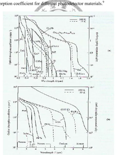
Light can be extremely transparent for long wavelengths without photoexitation, thus determining the quantum efficiency of a photodetector. Figure 2.3 shows the measured intrinsic absorption coefficient for different photodetector materials.9
Fig. 2.3 Optical absorption coefficients for many photodetector materials.
The photocurrent of a photodetector under illumination should be maximized for sensitivity. The basic metric is the quantum efficiency, defined as following equation,
opt ph ph
P h q I q
I
(2.2)where Iph is the photocurrent, Φ is the photon flux (=Popt/hν), and Popt is the optical power. The ideal quantum efficiency is unity. Another similar metric is the responsivity
, which is defined as following equation
24 . 1
) ( m h
q P
I
opt
ph
(A/W) (2.3)
where is the responsivity, and η is the quantum efficiency as statement in Eq. (2.2).
2.2.2 Photoconductor
As shown in Fig. 2.4,10 a photoconductor consists of a slab of semiconductor with ohmic contacts at both ends of the slab. When the surface of photoconductor is illuminated, electron-hole pairs are generated either by intrinsic or extrinsic transitions,
resulting in an increase in conductivity which is given by
)
( n p
q
n
p
(2.4)The increase in conductivity under illumination is mainly due to the increase in the number of electron-hole pairs.
Fig. 2.4 Schematic diagram of photoconductor.
2.2.3 Photodiode
A photodiode is basically a p-n junction or a metal semiconductor contact operated under reverse bias. When the light illuminated the photodiode, it has a depletion region with a high electric field that serves to separate photogenerated carriers and electric current flows in the external circuit. The depletion region should be kept thin to reduce the transit time, when the photodiode for high-frequency operation. In order to increase the quantum efficiency, the depletion layer must be sufficiently thick to absorb the incident light. Thus, there is a trade-off between the response speed and quantum efficiency. The quantum efficiency mentioned previously is the number of electron-hole pairs generated per incident photon (Eq. 2.2). A related merit is the
responsivity, which is the ratio of the photocurrent to the optical power (Eq. 2.3). One of the important factors that determine quantum efficiency is the absorption coefficient.
Since the absorption coefficient is a strong function of the wavelength, the wavelength range in which appreciable photocurrent can be generated is limited.
Most photodiodes use intrinsic photoexcitation, the long-wavelength cutoff λc is established by the band gap (Eq. 2.1). For wavelength longer than the cutoff wavelength, the values of absorption coefficient are too small to give appreciable absorption. The short-wavelength cutoff of the photoresponse comes about because the values of absorption coefficient are very large (more than 10-5cm-1), and the radiation is mostly absorbed very near the surface. Hence, the electron-hole pairs can recombine before they are collected in p-n junction. 9 There exists many types of photodiodes, and we will introduce in the following.
a. p-i-n Photodiodes
The p-i-n photodiode is a special case of the p-n junction photodiodes, and is one of the most common photodetectors, because the depletion region thickness can be designed to optimize the frequency response and the quantum efficiency.
b. Metal Semiconductor Photodiodes
A metal semiconductor photodiode is a high efficiency photodetector. The photodiode can be operated in two modes, depending on the incident photon energy9:
1. For the photon energy large than Eg, as shown in Fig. 2.5 (a), the radiation produces electron-hole pairs in the semiconductor.
2. For qφ<hν<Eg, as shown in Fig. 2.5 (b), the photoexcited electrons in the metal side can surpass the barrier and be collected by the semiconductor.
Fig. 2.5 (a) Band to band excitation of electron-hole pair (b) Internal photoemission of excited electron from metal to semiconductor.
c. Heterojunction Photodiodes
A heterojunction photodiode is formed by depositing a large band gap material epitaxially on a smaller-bandgap semiconductor. One major advantage of a heterojunction photodiode is that the quantum efficiency does not critically depend on the distance of the junction from the surface, because of a large bandgap material can be treating as a window for transmission of incoming optical power. Besides, the heterojunction can provide unique material combinations, so that the response speed
and quantum efficiency can be optimized for a given optical wavelength. Another advantage is reducing dark current.
2.3 Antireflection structure
2.3.1 Introduction
Multilayered coating of dielectric materials with different refractive indices is a popular technique and widely used as antireflection layer.11 However, a multilayered thin film has some disadvantages associated with limitations in the coating materials and various physical and chemical properties that will affect thermal mismatch and the stability of the thin film stack.12
The subwavelength surface (SWS) has a surface-relief grating with a period smaller than the wavelength of light, so it behaves as an antireflection surface.13-14 Particularly, for the structure with a tapered grating, the SWS suppresses reflection over a wide spectral bandwidth and a large field of view. This structure is more stable and has greater heat resistance than the multilayered thin film since it is fabricated from a single material. The schematic view of antireflection SWS surface is shown in Fig.
2.6.11
Fig. 2.6 Schematic diagram of SWS.
Because we would like to achieve high performance, the structural periodicities of SWS have to be smaller than the incident wavelength. A deep tapered shape of SWS surfaces is also important to obtain a broadband antireflection and its antireflection properties are improved by increasing the depth and decreasing the grating period.
There are some brief explanations by the graded refractive index model of antireflection for SWS surface.11 Fresnel reflection is generated mainly by the dramatically change of the refractive index at the boundary between the material and its surrounding medium.
Therefore, the reflection becomes low due to the change of the effective refractive index gradually. These SWS surfaces may be attractive for many applications such as solar cells, light-emitting diodes, and photodetectors, especially for solar collectors and for use in space, where stability and durability are the main concerns.
2.3.2 Theory of antireflection
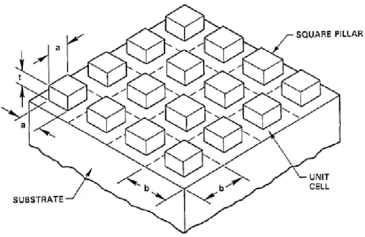
15At the Si-air boundary, however, a large amount of the Fresnel reflection loss is caused by the large difference in refractive index values. In order to suppress the Fresnel reflection at an optical surface, the SWS surface was used. A simple way of reducing Fresnel reflection at an optical surface is to apply a single quarter-wave layer as show in Fig. 2.7
Fig. 2.7 Geometry of the pillar array.
Using rigorous coupled wave analysis, Gaylord showed that when the electric field component is parallel to the grooves, the effective refractive index is
12 2
) 1
(
sparallel
f fn
n
(2.5)On the other hand, with the electric field perpendicular to the grooves, the effective
12 2
) / 1
(
slar
perpendicu
f f n
n
(2.6)where ns is the refractive index of substrate, f is the volume fraction of the substrate forming the grooves, as shown in Fig. 2.7, the volume fraction is
2 2
b
f a (2.7)
Owing to the structure symmetry, the effective index will be the same for both incident polarization components. Because the precise effective refractive index for the pillars is
unknown, he assumed a 50% dielectric constant mixture of the values given in Eqs.2.5 and 2.6. Squaring and averaging Eqs. 2.5 and 2.6, and then he find that the predicted polarization independent effective refractive index is
12 2
2 2 2
) 1 ( 2
) 1 ( 1
s
s s s
n f f
n n f f
fn n f
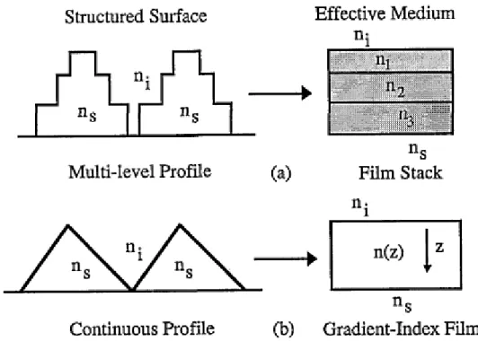
(2.8)For the specific case of a multilevel surface relief profile [see Fig. 2.8 (a)], the effective medium is a film stack where each layer of the film stack corresponds to a distinct level of the surface-relief profile. And we can calculate the effective refractive index by using Eq. 2.8. For a continuous profile [see Fig. 2.8 (b)], the effective medium is a gradient film.16
Fig. 2.8 Effective mediums: (a) a multilevel surface profile the effective medium is a film stack (b) for a continuous surface profile the effective medium is a grandient-index film.
Fig. 2.9 Graded refractive index model.
In summary, the spectral properties of antireflection SWS surface can be briefly explained by the graded refractive index model,11 which is showed in Fig. 2.9. And the reflectivity can be calculated by using Eq. 2.9,17 which the light is the normal incident.
2
i s
i s
n n
n
R n
(2.9)where the ns and ni are the refractive index of substrate and air, respectively.
2.4 Photoluminescence (PL) Spectroscopy
18-21In order to emit radiation from a semiconductor material, it must be energized by some external means. The most popular one way is by absorption of photons with energy larger than the band gap of semiconductor material. The resulting process, in which photon with energy lower than the excitation photons are radiated, is well known as photoluminescence (PL). Photoluminescence (PL) measurement is a very powerful and useful optical technique in semiconductor industry. Because of its sensitive ability, we could find the emission mechanism and band structure in semiconductors. Besides, photoluminescence can also detect the affects of impurity and defect in many compound semiconductor materials, which influences crystallization and device performance. The impurity type in the material can be understood by using a single PL spectrum. In some another researches, the halfwidth of PL peaks could be treated as an indication of sample crystallinity and quality, even though the analysis has not yet become highly quantitative. Eventually, by PL measurement, the stress inside sample can be investigated, including magnitude and direction.
2.4.1 Photoluminescence Emission
A photon with energy equals/exceeds to the band gap can excite electron from valence band to across the gap, and finally reaches the conduction band. These
processes are useful probes for band structures and detecting impurities in semiconductor. When the excited electron returns to the initial state, the process is called recombination. During the radiative mechanism, it radiated a photon with energy of the difference between the excited and the initial state energy.
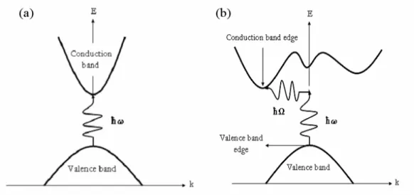
The fundamental absorption processes depend on whether the gap is direct or indirect. For example, GaAs is a direct band gap semiconductor material, an electron at the maximum state of valence band executes a vertical transition to the minimum state of conduction band directly as shown in Figure 2.10 (a). Energy is conserved according to the following equation:
i
f
E
E
(2.10)where Ei and Ef are the energies of initial and final initial state ,respectively, and is photon energy. In an indirect gap material such as Si, owing to the momentum conservation law, the excited electron needs additional momentum (phonon) to reach the minimum of conduction band at a non-zero wavevector (Figure2.10 (b)) position.
Then the equation of energy conservation is:
E
fE
i (2.11) where is the phonon energy, and the plus and minus signs are phonon emission and absorption, respectively.Fig. 2.10 (a) The lowest point of conduction band localizes at the same value of K as
the highest point of the valence band. The threshold frequency w for absorption phonon is given by the band gap. (b) The indirect transition involves both photon and phonon, because the band edges of the conduction bands and valence bands are separated in K space. The absorption threshold for the indirect transition is at Eg .
2.4.2 Recombination Processes
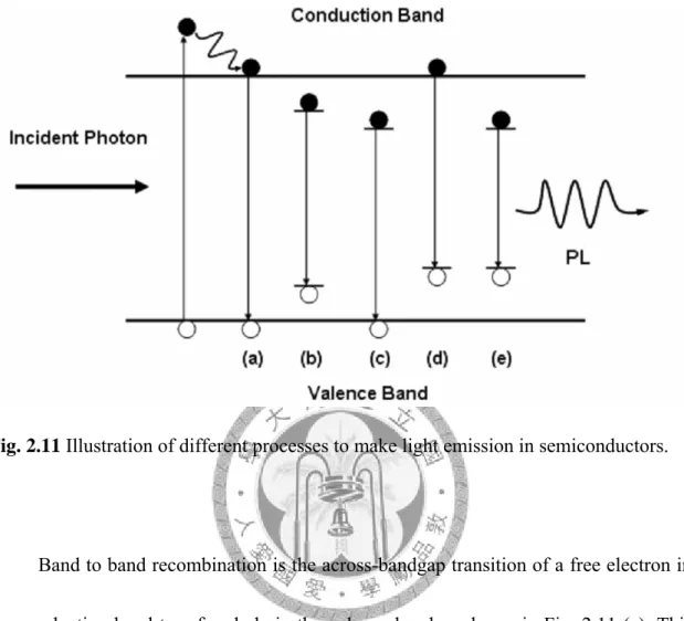
Fig. 2.11 illustrates the process of photo excitation and recombination. We are going to discuss recombination processes which can cause light emission. Figure 2.11 shows the five process of light emission due to the photo recombination:
(a) band to band recombination.
(b) excitationic recombination.
(c) free hole-neutral donor recombination.
(d) free electron recombination with a hole on a neutral acceptor.
(e) donor-acceptor recombination.
Fig. 2.11 Illustration of different processes to make light emission in semiconductors.
Band to band recombination is the across-bandgap transition of a free electron in the conduction band to a free hole in the valence band as shown in Fig. 2.11 (a). This emission occurs at the energies equal to or greater than the band gap. Recombination at energies greater than the band gap is due to the recombination of hot carriers which have not fully relaxed to the bottom (top) of the conduction (valence) band prior to recombination. If a intrinsic semiconductor material, the recombination will between electrons in the conduction band and holes in the valence band. If the temperature is sufficiently low (e.g., less than 25 K for GaAs), the electron-hole pairs can form a bound state in a hydrogen-atom-like formula, forming an exciton. Free electrons and
holes may become bounding owing to the Coulomb interaction to form free excitons, which are the lowest energy intrinsic quasiparticle states in a semiconductor material. If the semiconductor material contains impurities, several recombination paths are produced due to impurity states. Free-to-bound transitions involve the radiative recombination of a free carrier with another carrier bound to an impurity. There are two varieties: donor-to-valence band and conduction band-to-acceptor, which emission primarily occurs at energies less than the bandgap.
2.5 Raman Spectroscopy
18-21Raman scattering effect is one of inelastic scattering phenomenon of light with materials, which first observed this effect by Indian physicist, C.V. Raman. It involves a change in photon frequency. When light illuminates on the surface of material, it will mostly be reflected, transmitted, absorbed, or Rayleigh scattered. Owing to the first-order elastic interaction with electrons, phonons, and impurities, there is no change in photon frequency during these elastic interactions. However, a small fraction of the light interacts inelastically with phonon modes producing outgoing photons whose frequencies are shifted from the incoming values. These are the Raman-scattered photons. This interaction of incident light with optical phonon is called Raman scattering.
All the main Raman parameters such as band frequencies, intensities, line shape, linewidth and polarization behavior can be used to characterize the lattice, impurities, and free carriers in a semiconductor material. The intensity gives information about crystallinity, because of it may be reduced in the crystals damaged by ion bombardment or other means. The linewidths increase stand for a material is damaged or disordered, since these conditions increase phonon damping or change the rules for momentum conservation in the Raman process. The strengths and frequencies of the Raman phonon bands can determine the degree of alloying in a ternary material like AlxGa1-xAs. The frequencies of the longitudinal plasmon modes give the carrier density. All of these capabilities can be used for layered microstructures and bulk materials, subject only to the limitation that the penetration depth of the exciting radiation ranges from a few hundred nanometers (nm) to a micrometer (μm). However, a change in the wavelength of the exciting radiation changes the penetration, giving flexibility in the probe depth.
The noted method of Raman spectroscopy support quantitative microanalysis without destroying the device. It provides the information about the characterization of semiconductors damaged by ion implantation, of strain in heterostructures, determination of crystal orientation and the measurement of free-carrier density.
2.5.1 Anti-Stokes and Stokes lines
Unlike absorption spectroscopy, Raman scattering involves a change in photon frequency. A small part of the light interacts inelastically with phonon modes, producing outgoing photons whose frequencies are shifted from the incoming values.
These are the Raman-scattered photons. They gain energy by absorbing a phonon (anti-Stokes shifted), or lose energy by emitting one phonon (Stokes shifted) as show in
Fig. 2.15, according to the energy and momentum conservation rules:
i
s w
w
k q
qs i (2.12)
Fig. 2.12 The diagram shows the conservation rules for Raman scattering.
where ws, wi, qs, and qi are the incoming photon frequencies, scattered photon
frequencies, incoming photon wavevectors and scattered photon wavevectors respectively, and Ω andk are the phonon frequency and wavevector respectively.
Raman scattering isinherently a weak process, but laser provide enough power that the spectra can beroutinely measured.
The full theory of Raman scattering is complex. This is one reason for detailed line-shape analysis is not often used for this kind of spectroscopy. A simple picture, however, makes the basic process understandable. The frequency-shifted photons can be described as carrying side-bands at the phonon frequency, which arise from the nonlinear interaction between the radiation and the semiconductor lattice.
Cardona points out the classical theory of this nonlinear Raman interaction depends on the polarizability of the lattice, which is the change in its electric susceptibility χ because of excitation of the crystal. The dipole moment induced by the radiationelectric field is:
....
) 2( ) 1 ( )
( 22 2
u E
u d uE d du E d w
P (2.13)
where u is a coordinate describing the phonon modes, and (w) is dielectric
function of frequencies. The phonon coordinate for a mode with frequency Ω has the form, u u0cost whereas the incoming electric field has the form E E0coswt. Then the induced dipole moment contains terms
cost
ncoswt, where n=1, 2, 3…From standard trigonometric identities, these terms can be expressed in an alternate
form
,...
3 , 2 , 1 ,
)
cos( w n t n
(2.14)such that the light re-radiative by the oscillating polarization vector has components at the frequencies ω ± nΩ . The leading term represents Raman-shifted bands at frequency ω + nΩ and ω − nΩ to the anti-Stokes and Stokes lines.
The two Raman single-phonon bands, the Stokes modes at ω-Ω are the stronger, which dominate in measurements. The mode strengths depend on the number of phonons available, which is a count of the distribution of normal mode harmonic oscillators in the lattice versus temperature. The results can be derived from the matrix element for phonon creation or annihilation, which depends on nk, the number of phonons of wavevector k, and follows the Planck distribution function
1 1
T k k
e
bn
(2.15)where T is temperature, the relative strength of the lines can be calculated as :
T k k
k stokes
stokes
anti e B
n n w
I w I I
I
1 )
(
)
(
(2.16)Aa T 0, the anti-Stokes line vanishes, and the Stokes line dominates at actual measurement temperatures.
References
1. Ü. Özgür, Ya. I. Alivov, C. Liu, A. Teke, M. A. Reshchikov, S. Doğan, V. Avrutin, S.-J. Cho, and H. Morkoç, J. Appl. Phys. 98, 041301 (2005).
2. Lei Luo, Yanfeng Zhang, Samuel S. Mao, and Liwei Lin, Sensors and Actuators A
127, 201 (2006).
3. C. H. Park, I. S. Jeong, J. H. Kim, and Seongil lm, Appl. Phys. Lett. 82, 3973 (2003).
4. J. D. Ye, S. L. Gu, S. M. Zhu, W. Liu, S. M. hang, Y. Shi, and Y. D. Zheng, Appl.
Phys. Lett. 88, 182112 (2006).
5. Ya-Ping Hsieh, Hsin-Yi Chen, Ming-Zhang Lin, Shu-Chia Shiu, Mario Hofmann, Ming-Yau Chern, Xiaoting Jia, Ying-Jay Yang, Hsiu-Ju Chang, Hsuan-Ming Huang, Shao-Chin Tseng, Li-Chyong Chen, Kuei-Hsien Chen, Ching-Fuh Lin, Chi-Te Liang, and Yang-Fang Chen, Nano Lett. 9, 1839 (2009).
6. I. T. Drapark, Semiconductors 2, 624 (1968).
7. Ya. I. Alivov, D. C. Look, B. M. Ataev, M. V. Chukichev, V. V. Mamedov, V. I.
Zinenko, Yu. A. Agafonov, and A. N. Pustovit, Solid-State Electron. 48, 2343 (2004).
8. I. S. Jeong, J. H. Kim, and S. Im, Appl. Phys. Lett. 83, 2946 (2003).
9. S. M. Sze, and Kwok K. Ng, Physics of Semiconductor Devices, 3nd ed (Wiley,
New York, 2007).
10. S. M. Sze, Semiconductor Devices (Physics and Technology), 2nd ed (Wiley, New York, 2001).
11. Yoshiaki Kanamori, Ken-ichi Kobayashi, Hiroo Yugami, and Kazuhiro Hane, Jpn. J.
Appl. Phys 42, 4020 (2003).
12. Y. Kanamori, M. Sasaki, and Hane, Optics Letters 24, 1422 (1999).
13. Y. Kanamori, K. Hane, H. Sai, and H. Yugami, Appl. Phys. Lett. 78, 142 (2001).
14. Sen Wang, Xiao Zheng Yu, and Hong Tao Fan, Appl. Phys. Lett. 91, 61105 (2007).
15. M. E. Motamedi, W. H. Southwell, and W. J. Gunning, Applied Optocs 31, 4371 (1992).
16. Daniel H. Raguin, and G. Michael Morris, Applied Optics 32, 1154 (1993).
17. Hecht, Optics 3nd ed (Addison Wesley, 1998) p.119.
18. S. Perkowitz, Optical Characterization of Semiconductors: Infrared, Raman, and Photoluminescence Spectrosocpy (Academic Press, 1993).
19. C. Kittel, Introduction to Solid State Physics (Seventh Edition).
20. R. A. Stradling and P. C. Klipstein, Growth and Characterization of Semiconductors.
(Adam Hilger:September 1989).
21. J. R. Lakowicz, Principles of Flurescence Spectroscopy (Academic, New York 1999).
Chapter 3
Experimental Details
Chapter 3 Experimental Details
3.1 Photoluminescence Apparatus
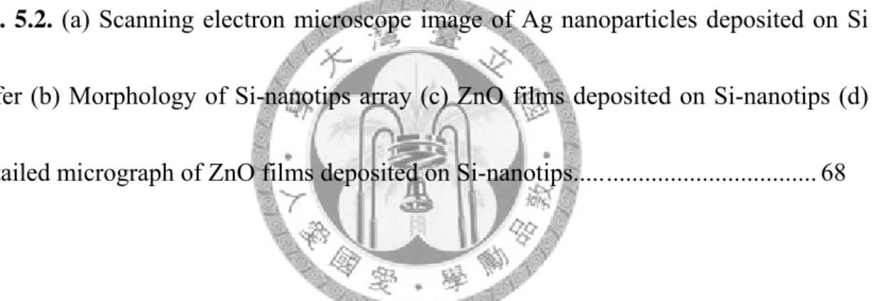
The PL technique is the most straightforward measurements in optics which is shown in Fig. 3.1. The excitation source is laser, or xenon lamp whose photon energy is higher than the band gap energy of the semiconductor materials to be examined. In our laboratory, He-Cd laser with 325 nm and xenon lamp are used to be the excitation source. We have to choose an adequate excitation source with suitable intensity. The PL signal passes through focal lens to enhance the collected photons and be sent to a monochromator to select a wavelength to transmit to the detector, usually a photomultiplier tube. The resolution of the system, its ability to accurately measure energy, is determined by the focal length of the monochromator, whereas the grating spacing sets the wavelength coverage. The sample is placed inside a cryostat to keep at our desire temperature and obtained the better signal-to-noise ratio. At long wavelength a photomultiplier tube with a GaAs or other composite cathode is useful. At different wavelength, a different photodiode is used.
Fig. 3.1 Conventional PL setup.
3.2 Raman Scattering Apparatus
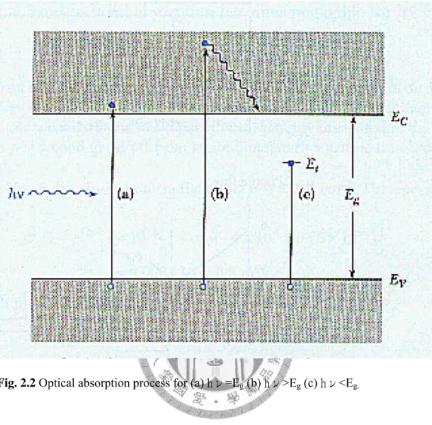
There are two main factors that affect the design Raman spectrometers. One is the weakness of the signal compared with the much larger PL signal shown in Figure 3.3, which also shows that Raman and PL data can be obtained with the same optical arrangement. The other one is that this weak signal is spectrally very near the order-of-magnitude larger exciting laser signal. The typical Raman shift ω(phonon)/ω (laser) is only about 1%. This indicates that the feeble Raman peaks must be measured against a background of intense Rayleigh scattering. Therefore, Raman measurements require the strongest available sources (without damaging the sample), well-designed optics to filter out the undesired Rayleigh peak, and excellent detectors to record the few Raman-shifted photons.
Fig. 3.2 The diagram illustrates the small Raman intensity compared with the signal
from a strong PL emitter. It also shows that both PL and Raman data can be obtained with the same experimental arrangement.
A typical Raman arrangement is similar to that for PL with one major difference:
the single monochromator used for most PL work does not discriminate sufficiently to separate the Raman signal from the strong Rayleigh light that accompanies it. The double monochromator is needed in order to increase discrimination, which consists of two ganged gratings turning together and sequentially selecting the light. In some case, for instance to examine Raman peaks within a few wavenumbers of the exciting line, triple monochromator must be used. Besides, the Raman system may also include means to polarize the exciting light and analyze the polarization of the scattered light.
These polarization states are intimately connected to the orientation of a crystalline sample.
In the variation of Raman characterization called microprobe Raman scattering.
The T64000 micro-Raman system we used is produced by the Jobin-Yvon Company.
The exciting laser light is coupled to the sample by means of a microscope, which focuses the light to a spot as small as approximately 1μm. As shown in Figure 3.3, the optics can be arranged so that the Raman scattered light is coupled to the monochromator through the microscope and auxiliary illuminating light is sent to a video camera to give a real-time image of the sample surface. This makes it possible to locate and probe areas of the sample as small as the bean size. This method can also be applied to the PL called the micro-PL measurement, which is helpful to the optical measurements in nanoscale materials. The microprobe technique is becoming widely used to examine materials and devices.
Fig. 3.3 The schema of a Raman microscope. The microscope objective lens focusesthe laser beam to a spot size of about 1um. Scattered light is transmitted through thebeam splitter to the double monochormator, giving the Raman spectrum of the selected region.
Visible light from the illuminator is reflected from the sample to a video camera, giving a realtime image to the allow position of the probe beam. The sample can be moved on the x-y stage.
3.3 DC Sputtering Deposition
Early days, the method of sputtering deposition was used to deposit the thin film, or applying the metal in the fabric. When the vacuum technology matures, the sputtering is largely replaced by the evaporation, due to the rate of latter is faster than the former. However, many materials are unable to evaporate by heating the resistance, so this method is still extensively used to produce the composite. A sputtering system (JFC-1600, JEOL) is used in this work. As shown in Fig. 3.4, during sputtering, the substrate is placed in a vacuum chamber with a target of the material to be deposited.
The plasma is generated in a passive source gas (i.e. Argon) in the chamber and the ion bombardment is directed towards the target, causing material to be sputtered off the target and condense on the chamber walls and the substrate. A strong magnetic field (magnetron) can be used to concentrate the plasma near the target to increase the deposition rate.
Fig. 3.4 A schematic illustration of the apparatus of DC sputtering deposition.
3.4 Reactive Ion Etching
Reactive ion etching (RIE) is an etching technology used in microfabrication for anisotropic etching. It uses chemically reactive plasma to remove material deposited on wafers. The plasma is generated under high vacuum by an electromagnetic field.
High-energy ions from the plasma attack the wafer surface and react with it.
RIE system consists of a cylindrical vacuum chamber, with a wafer platter situated in the bottom portion of the chamber. The wafer platter is electrically isolated from the rest of the chamber, which is usually grounded. Gas enters through small inlets in the top of the chamber, and exits to the vacuum pump system through the bottom.
The types and amount of gas used vary depending upon the etch process such as CF4
used for etching silicon. Gas pressure is typically maintained in a range between a few millitorr and a few hundred millitorr by adjusting gas flow rates and/or adjusting an exhaust orifice. Figure 3.5 shows a diagram of a RIE setup of OXFORD instruments Plasmalab 80 Plus.
(a) (b)
Fig. 3.5 The RIE system of Plasmalab 80 Plus: (a) an overall view (b) a schematic of reacting chamber with two parallel plates and a few hundred watts of RF electromagnetic field applied on it.
3.5 Evaporation
Evaporation is a general method of thin film deposition. The source material is evaporated in a vacuum. The vacuum allows vapor particles to travel directly to the substrate, where they condense back to a solid state. Evaporation is used in microfabrication, and to make macro-scale products.
Evaporation involves two basic processes: a hot source material evaporates and condenses on the substrate. Evaporation takes place in a high vacuum, i.e. vapors other than the source material are almost entirely removed before the process begins. In high
vacuum, evaporated particles can travel directly to the deposition target without colliding with the background gas (with a long mean free path). When evaporation is performed in poor vacuum or close to atmospheric pressure, the resulting deposition is generally non-uniform and tends not to be a continuous or smooth film. On the other hand, the evaporation material may be oxidized in poor vacuum and deposited on the substrate.
Any evaporation system includes a vacuum pump system with the combination of several kinds of pump, such as diffusion pump, mechanical pump, and turbo pump. It also includes an energy source that evaporates the material to be deposited. In the thermal method, the source material is placed in a crucible, which is radiatively heated by an electric filament. A common way is to put source material on a tungsten boat and transmit large current through the boat to evaporate the material. In the e-beam evaporation, the source is heated by an electron beam with energy up to 15 keV. Figure 3.6 shows typical thermal and e-beam evaporation machines.
(a) (b)
Fig. 3.6 An overall view of (a) the thermal evaporation machine (b) the e-beam evaporation machine.
3.6 Scanning Electron Microscopy
Electron microscope utilizes an electron beam to produce a magnified image of the sample. There are three principle types of electron microscopes: scanning, transmission, and emission. In the scanning and transmission microscope, an e-beam incident on the sample produces an image while in the field-emission microscope the specimen itself is the source of electrons. Scanning electron microscopy (SEM) is similar to light microscopy with the exception that electrons are used instead of photons and the image photons and the image is formed in a different manner. A SEM consists
of an electron gun, a lens system, scanning coils, an electron collector, and a cathode ray display tube (CRT). The electron energy is typically 10-30 KeV for most samples, but for insulating samples the energy can be as low as several hundred eV. The use of electrons has two main advantages over typical microscopes: much larger magnifications are possible since electron wavelengths are much shorter than the photon wavelengths and the depth of field is much higher.
De Broglie proposed in 1923 that particles can also behave as waves. The electron wavelength λe depends on the electron velocity v or the accelerating voltage V as
V qmV
h mv
h
e
22 . 1
2
(3.1)The wavelength is 0.012 nm for V=10000 (v), a wavelength significantly below the 400 to 700 nm wavelength range of visible light – making the resolution of an SEM much better than that of an optical microscope.
The contrast in a SEM depends on a number of factors. For a flat, uniform sample the image shows on contrast. If, however, the sample consists of materials with different atomic numbers, a contrast is observed if the signal is obtained from the backscattered electrons, because the backscattering coefficient increases with the atomic number Z.
The secondary electron emission coefficient, however, is not a strong function of Z and atomic number variations give no appreciable contrast. Contrast is also influenced
feature is the sample topography. Secondary electrons are emitted from the top 10 nm or so of the sample surface. When the sample surface is tilted from the normal beam incidence, the electron beam path lying within this 10 nm is increased by the factor1/cosθ, where θ is the angle from the normal incidence (θ = 0° for normal incidence). The interaction of the incident beam with the sample increases with path length and the secondary electron emission coefficient increases. The contrast C depends on the angle as C tan()d .
For θ = 45° , a change in the angle of dθ = 1° produces a contrast of 1.75% while at 60°
the contrast increase to 3% for dθ = 1°.
The beam diameter of SEMs is in the range of 1 to 10 nm. Yet the resolution of e-beam measurements is not always that good. Why is that? It has to do with the shape of the electron-hole cloud generated in the semiconductor. When electrons impinge on a solid, they lose energy by elastic scattering and inelastic scattering. Elastic scattering is caused mainly by interactions of electrons with nuclei and is more probable in high atomic number materials and at low beam energies. Inelastic scattering is caused mainly by scattering from valence and core electrons. The result of these scattering events is a broadening of the original nearly collimated, well-focused electron beam within the sample.
The generation volume is a function of the e-beam energy and the atomic number
Z of the sample. Secondary electrons, backscattered electrons, characteristic and continuum X-rays, Auger electrons, photons, and electron-hole pairs are produced. For low-Z samples most electrons penetrate deeply into the sample and are absorbed. For high-Z samples there is considerable scattering near the surface and a large fraction of the incident electrons is backscattered. The shape of the electron distribution is
“teardrop”-shaped, as shown in Fig. 3.7. As Z increase (15<Z<40) the shape becomes more spherical and for Z>40 it becomes hemispherical. “Teardrop” shapes have been observed by exposing polymethylmethacrylate to an electron beam and etching the exposed portion of the material. Electron trajectories, calculated with Monte Carlo techniques, also agree with these shapes.
Fig. 3.7 Summary of the range and spatial resolution of backscattered electrons, secondary electrons, X-rays, and Auger electrons for electrons incident on a solid
The depth of electron penetration is the electron range Re, defined as the average total distance from the sample surface that and electron travels in the sample along a trajectory. A number of empirical expressions have been derived for Re. One such expression is
) 10 (
28 .
4 6 1.75 E cm Re
(3.2)
where ρ is the sample density (g/cm3) and E the electron energy (KeV).
Chapter 4
Fabrication and Characterization of
Si-nanotips Array
Chapter 4 Fabrication and Characterization of Si-nanotips Array
4.1 Introduction
Antireflection techniques play an important role for many optoelectronic devices, such as solar cells, displays, and light sensors.1-4
One of popular methods to suppress the reflection is surface coatings. And another one is to use a SWS as an antireflection layer. The SWS is the surface-relief grating with the period smaller than the light wavelength, behaves as an antireflection surface.5-8 However, there are problems of surface coating such as thermal mismatch, adhesiveness, and stability. So an alternative to surface coatings is the surface-relief structures with subwavelength structures (SWS).
The SWS can solve the above problems of surface coatings due to the same material constitutions as the substrate. According to previous reports, they show that the reflectivity can be suppressed for a wide spectral bandwidth. In this work, we use relative ion etching with Ag nanopaticles as a mask to fabricate Si-nanotips with SWS surface to suppress the reflection. We will discuss the different antireflection characteristics for the SWS surface obtained from different RIE times.
4.2 Experiment
The fabrication procedure of Si nanotips array with SWS surface is schematically
shown in Fig.4.1. Firstly, p-type (100) Si wafer with a resistivity of 10 ohm was cut into 1×0.5 cm2 used as the substrate. Before the fabrication, the Si substrate was ultrasonically cleaned with acetone, methanol and DI water for 3 min, and Piranha Clean process (SPM) composed of H2SO4/H2O2 (4:1) was used to clean organic substance under 130℃ for 10 min. The wafers were then dipped in buffer oxide etching (BOE, 1:6) to remove the native oxide, and they were cleaned with DI water.
sputter Ag film and
anneal to form Ag nanoparticles
dry etching by RIE Si wafer
Removal of residual Ag Si-nanotips
sputter Ag film and
anneal to form Ag nanoparticles
dry etching by RIE Si wafer
Removal of residual Ag sputter Ag film and
anneal to form Ag nanoparticles
dry etching by RIE Si wafer
Removal of residual Ag sputter Ag film and
anneal to form Ag nanoparticles
dry etching by RIE Si wafer
Removal of residual Ag Si-nanotips
Fig. 4.1 Schematic diagram for the fabrication procedure.
Secondly, an Ag thin film about 10 nm was deposited onto the p-Si wafer by using DC sputtering technique (JEOL, JFC-1600 auto fine coater). Then, they were put into a furnace and annealed for 10 min at different temperatures of 300, 400, 500, and 600℃, to form Ag nanoparticles which will serve as the etching mask in the following process. The Si wafer was then etched by using reactive ion etching (RIE) equipment (Oxford plasma 80 plus) at the CF4 flow rate of 40 sccm, the pressure is 25 mtorr, and the RF power is 100 W. To generate Si nanotips array with different heights, etching times of 10-40 min were used. After dry etching by RIE, the substrate was dipped in HNO3 (10%) solution in order to remove the residual Ag nanoparticles. Finally, the sample was immersed in BOE (1:6) to remove silicon oxide, which was formed by HNO3 clean step.
4.3 Results and discussion
Figure 4.2 shows the etching mask of Ag nanoparticles after the Ag film was annealed at different temperatures of 300, 400, 500, and 600℃. Under 300℃ condition, it shows the Ag film can not form Ag nanoparticles, because of the temperature is not high enough to change the Ag film into Ag nanoparticles. Under 400℃ condition, the formed Ag nanoparticles show anomalous shape instead of circular. Because the temperature is not high enough, silver intermolecular cohesive force is not big enough.
From this reason, the Ag nanoparticles possess an anomalous shape.
(a)
(b)
Fig. 4.2 Scanning electron microscope images of Ag nanoparticles deposited on Si wafer at different temperatures (a) 300℃ (b) 400℃ (c) 500℃ (d) 600℃
(c)
(d)
At 500℃, the nanoparticles size of ranges from about 10 nm to 100 nm, and the distribution is even. When the temperatures increase to 500℃ and 600℃, the Ag intermolecular cohesive force is enough to cause the Ag film to contract the circular pellet. Under 600℃ condition, the diameter and distance of Ag nanoparticles were both larger than 500℃ condition. From the above discussion, we choose the thermal dewetting of 500℃ to process the dry etching by using RIE. Figure 4.3 shows the scanning electron microscopy (SEM) images for the fabricated Si nanostructures with different etching times. With increasing of the RIE time, the dimensions of the nanotips decrease and the grooves of the nanotips grow deep, which is shown in table 4.1 and figure 4.4. The heights of Si nanotips were measured to be 143, 315, 361 and 402 nm for etching times of 10, 20, 30 and 40 min, respectively. As the RIE times increased, the nanotips become concentrated, and the appearance of Si nanotips varied from flat to sharp. From figure 4.3, we discovered that the Si nanorods were formed when the etching times have the values of 10 and 20 min. With increasing RIE times to 30 and 40 min, the Si nanotips were formed, and the Si-nanotips have a conical profile. To analyze the light trapping effect of Si-nanotips array, the reflectivity was measured. Figure 4.5 exhibits the reflectivity of wavelength dependence from 350~750 nm for Si substrate, Si-nanotip with etching time of 10, 20, 30, and 40 min, and the corresponding reflectivity is 45%, 8.6%, 6.2%, and 2.8%, respectively.
(a)
(b)
Fig. 4.3 Morphology of Si-nanotips array fabricated by RIE with different times (a)10min (b) 20 min (c) 30 min (d) 40 min
(c)
(d)
Fig 4.4 The grooves deep of Si nanotips array in different RIE times.
Table 4.1 Detailed list of Si nanotips grooves deep.
Etching time 10min 20min 30min 40min
Average depth 143nm 315nm 361nm 402nm
10 15 20 25 30 35 40
100 150 200 250 300 350 400
Depth (nm)
Etching time (min)