國 立 交 通 大 學
光電工程研究所
碩
士
論
文
可應用於太陽能電池之奈米結晶矽量子點埋入式摻鋁氧化
鋅薄膜與 p 型氧化鋅薄膜之特性研究
Characteristics of the Nano-crystalline Si Quantum Dots
Embedded in the Al-doped ZnO Thin Films and the p-type
ZnO Thin Films for Solar Cell Applications
研 究 生:莊文齡
指導教授:李柏璁 博士
可應用於太陽能電池之奈米結晶矽量子點埋入式摻鋁氧化
鋅薄膜與 p 型氧化鋅薄膜之特性研究
Characteristics of the Nano-crystalline Si Quantum Dots
Embedded in the Al-doped ZnO Thin Films and the p-type
ZnO Thin Films for Solar Cell Applications
研 究 生:莊文齡 Student:Wen-Ling Chuang
指導教授:李柏璁 博士 Advisor:Dr. Po-Tsung Lee
國 立 交 通 大 學
光電工程研究所
碩 士 論 文
A Thesis
Submitted to Department of Photonic and Institute of Electro-Optical Engineering College of Electrical Engineering and Computer Science
National Chiao Tung University In partial Fulfillment of the Requirements
for the Degree of Master in
Department of Photonic and Electro-Optical Engineering July 2011
Hsinchu, Taiwan, Republic of China
I
可應用於太陽能電池之奈米結晶矽量子點埋入式摻鋁氧化
鋅薄膜與 p 型氧化鋅薄膜之特性研究
研究生:莊文齡
指導教授:李柏璁 博士
國立交通大學光電工程研究所碩士班
摘
要
為了達到高效率、低成本的太陽能電池,全矽材料串接太陽能電池是很有潛 力的。將 不同能隙之矽奈米結晶量子點薄膜堆疊可減少高能量光子的損耗,以提 高效率。一般,大部分的實驗室會將矽奈米結晶埋在SiO2、Si3N4或SiC的材料中,但這些材料的導電性不好,造成此結構所形成之太陽能電池的效率比理論上低。 為了改善此問題,我們提出將導電性較好的摻鋁氧化鋅材料應用在矽奈米結晶量 子點薄膜中。 我們分析不同鋁含量對矽奈米結晶量子點薄膜的影響。當鋁的含量增加,奈 米結晶矽量子點的大小和矽結晶率會減少。鋁的摻雜會抑制矽的成長。而矽奈米 結晶量子點薄膜的導電性會隨著鋁含量增加而增加。但太粗糙的表面型態會使導 電性減少。在多層薄膜與矽基板界面處的氧化矽和退火完的薄膜彎曲等兩個問題 尚須解決。 為了解決界面氧化矽的問題,我們發展p型氧化鋅薄膜來取代矽基板。樣品 在適當的氮流量、工作壓力和退火條件製程下會具有p型特性。我們演示了氧化 鋅p-n同質接面並具有二極體的整流現象。 矽奈米結晶量子點埋入摻鋁氧化鋅薄膜的裝置成功演示出。若未來可解決界 面氧化層和退火完薄膜彎曲的問題,此裝置將有潛力應用於太陽能電池中。
II
Characteristics of the Nano-crystalline Si Quantum Dots
Embedded in the Al-doped ZnO Thin Films and the p-type
ZnO Thin Films for Solar Cell Applications
Student: Wen-Ling Chuang
Advisor: Dr. Po-Tsung Lee
Department of Photonics and Institute of Electro-Optical
Engineering, National Chiao Tung University
Abstract
In order to achieve high efficiency and low cost solar cells, all silicon-based tandem solar cells including the nano-crystalline silicon (nc-Si) quantum dots (QDs) are proposed. The nc-Si QD thin films stacking with different bandgaps can reduce the high energy photon loss, so the efficiency can be improved. In general, most groups will embed nc-Si QDs in the Si-based materials, such as SiO2, Si3N4, and SiC.
Because of poor conductivity of these materials, the efficiency is still substantially lower than the theoretical value. In this study, we propose to embed nc-Si QDs in the Al-doped ZnO (AZO) matrix.
We study the effect of the Al concentration on the nc-Si QD thin films. As the Al concentration increases, the nc-Si QD size and Si crystallinity decrease. The addition of Al suppresses the growth of Si. The conductivity of the nc-Si QD thin films increases with the increase of the Al concentration. However, the rougher surface morphology possibly causes the conductivity to decrease. The silicon oxide layer between the multilayer thin film and the Si substrate and the bending films after annealing are two problems need to be solved.
In order to solve the silicon oxide layer at the interface, we develop the p-type N-doped ZnO thin films to replace the Si substrates. The samples with suitable N2
flow, working pressure, and annealing conditions show the p-type properties. We demonstrate the ZnO p-n homojunction and examine the device has a diodelike rectification characteristic.
The device of the nc-Si QDs embedded in the AZO matrix has been demonstrated. If we solve the silicon oxide layer at the interface and bending films after annealing in the future, the device is a promising structure for solar cell applications.
III
Acknowledgements
首先,我想要感謝我的家人,於求學期間給予我支持與鼓勵,讓我有勇氣去 面對遇到的困難與挫折,使我在求學的 路上不感到孤獨。也特別感謝我的媽媽每 每在我回家的時候煮豐盛的食物把我餵得飽飽的,也不忘在我回新竹的時候幫我 準備滿滿的水果與營養品。 研究所的生活雖然只有短短 兩年,卻令我受益匪淺也印象深刻。不論是每一 次的實驗室聚餐、與夥伴們的吵吵鬧鬧、在排球場上的廝殺或半夜在奈米中心做 實驗,都讓我難以忘懷。雖然在研究過程中,遇到很多的挫折與失敗,但有實驗 室夥伴們的支持與幫助,及自己永不放棄的精神,使得研究終於有所成果。在此, 我特別感謝我的指導教授 李柏璁老師,感謝老師在這兩年中對於我實驗方面的指 導,使得在研究過程中遇到的難題得以解決。另外,我也很感謝光揚學長於我研 究的路上給予很多的建議與指導,讓我不至於走了太多的冤枉路,使我的研究順 利有所結果。此外,我還要感謝與我一起奮鬥的實驗室夥伴,感謝金剛、紹平、 立勛、雋崴、品睿在實驗中給予我的幫忙及鼓勵,感謝贊文、資岳、家揚、品佐、 佳裕學長們在實驗過程中的寶貴意 見,感謝權政、哲嶢、為智、開昊這群學弟妹 們,在我實驗忙碌過程中給予我幫助。 最後再一次感謝家人、老師和實驗室所有的夥伴們,讓我在這兩年碩士生活 活得精彩萬分,不留下一絲遺憾。也因為你們的幫忙及鼓勵,讓我的實驗順利有 所成果。 2011/08/18 於新竹 國立交通大學 交映樓 401 室IV
Content
Abstract (in Chinese)………I
Abstract (in English)……….……II
Acknowledgements……….……….III
Content……….………IV
List of Tables ………...VI
List of Figures ………....VII
Chapter 1 Introduction
1.1 Background………..1
1.2 Solar Cells………2
1.3 Solar Cells with Multiple bandgaps……….3
1.3.1 Power Loss Mechanisms………3
1.3.2 Effective Bandgap Engineering……….5
1.3.3 All Si-based Tandem Solar Cells………...6
1.4 Paper Review………...7
1.4.1 Al-doped ZnO Thin Films……….7
1.4.2 Nano-crystalline Silicon Quantum Dot Solar Cells…………...7
1.4.3 p-type ZnO Thin Films……….10
1.5 Motivation………...11
Chapter 2 Fabrication Process and Analyzing Method
2.1 Fabrication Process……….13
2.1.1 Substrate Clean……….13
2.1.2 Thin Film Deposition………14
2.1.3 Sample Annealing Process………...17
2.1.4 Electrode Deposition………...18
2.2 Analyzing Method………...18
2.2.1 Four-Point Probe………...18
2.2.2 Current-Voltage Measurements………19
2.2.3 High Resolution X-Ray Diffractometer………19
2.2.4 High Resolution Confocal Raman Microscope………20
V
Chapter 3 Characterization of the Nano-crystalline Si
Quantum Dots Embedded in the Al-doped ZnO Thin Films
3.1 Characterization of the Al-doped ZnO Thin Films………23
3.2 Influence of Different Annealing Temperatures………25
3.3 Influence of Different Al Concentrations………...27
3.4 Comparison of the Nano-crystalline Si Quantum Dots Embedded in
the ZnO and Al-doped ZnO Thin Films……….32
3.5 Problems of the
Nano-crystalline Si Quantum Dots Embedded in the
Al-doped ZnO Thin Films………..35
Chapter 4 Characterization of the p-type ZnO Thin Films
4.1 Analysis of High Resolution Confocal Raman Microscope………...39
4.2 Analysis of
Current-Voltage Characteristics………...41
4.3 Analysis of ZnO p-n Homojunctions………...45
Chapter 5 Conclusion and Future Work
5.1 Conclusion………...47
5.2 Future Work………...48
Reference
Vita
VI
List of Tables
Table 2.1: The sputtering parameters of undoped ZnO and AZO thin
films. ……….15
Table 2.2: The sputtering parameters of the [AZO/Si]
20multilayer thin
films. ……….16
Table 2.3: The sputtering parameters of p-type ZnO thin films. ...…17
Table 3.1: The concentration of atoms in the AZO thin films measured
by XPS. ...27
Table 3.2: The fitting results of the Raman curves for the samples
AZ5025-ML, AZ5075-ML, and AZ75-ML annealed at 1000
℃ for 5 minutes. ………..………29
Table 3.3: The fitting results of the Raman spectra for the samples
Z75-ML and AZ75-ML annealed at 1000 ℃ for 5
minutes. ………33
Table 4.1: The concentration of Zn, O and N atoms in the ZnO:N thin
VII
List of Figures
Fig. 1.1: Changes in global warming (blue, left-hand scale) and fossil
fuel consumption (red, right-hand scale) with
time. ……...1
Fig. 1.2: Three generations of photovoltaic technology: (I) Si
wafer-based; (II) thin-film; (III)
high-efficiency
thin-film. ………..……….3
Fig. 1.3: Power loss paths in a standard p-n junction: (1) low energy
photon loss, (2) high energy photon loss, (3) junction loss, (4)
contact loss, and (5) recombination loss. …...4
Fig. 1.4: Materials with different bandgaps absorb corresponding
wavelengths of the solar spectrum. ………...4
Fig. 1.5: Experimental bandgaps of Si QDs embedded in SiO
2and SiN
xfrom several authors. …….…………...……….6
Fig. 1.6: Schematic of (a) two-cell and (b) three-cell tandem solar
cell. ………...……….6
Fig. 1.7: The formation of nc-Si QDs in (a) a single Si-rich layer and (b)
a multilayer structure. ...……..………..8
Fig. 1.8: The energy band diagram of c-Si and its carbide, nitride and
oxide. …………..………..9
Fig. 2.1: Fabrication process of the nano-crystalline Si quantum dot
thin film. ……...………..13
Fig. 2.2: Preliminary RCA clean process of Si wafers. ……..……..14
Fig. 2.3: The structure of (a) undoped p-type ZnO, (b) Al-doped ZnO,
and (c) p-type ZnO thin films deposited on Si wafers. …...15
Fig. 2.4: Operation of sputtering during co-sputtering ZnO and AZO
targets. ………...………..16
Fig. 2.5: The structure of the multilayer thin films. …………....…..16
Fig. 2.6: Illustration of the formation of nc-Si QDs embedded in the
AZO matrix. ………...……….18
Fig. 3.1:
Transmittance and (b) plots of (αhν)
2versus (hν) for the AZO
and ZnO thin films annealed at 1000 ℃ for 5 minutes. The
inset in (b) shows the optical bandgaps of the samples. ...24
Fig. 3.2: Raman spectra of the sample AZ5075-ML annealed at
different temperatures. ……...……….……25
Fig. 3.3: (a) Transmittance and (b) absorbance spectra of the sample
VIII
AZ5075-ML annealed at different temperatures. …..…….26
Fig. 3.4: The example for how to find the optical bandbap. The sample
is AZ5075-ML annealed at 900 ℃ for 5 minutes. ..…..…26
Fig. 3.5: Raman spectra of the samples with different Al concentrations
annealed at 1000 ℃ for 5 minutes. ……..…...…..………28
Fig. 3.6: Raman spectra and fitting curve for the sample AZ5025-ML
annealed at 1000 ℃ for 5 minutes. The line (dash, red) is the
Raman spectra, while the line (solid, black) is the
corresponding fit. ………..…………..29
Fig. 3.7: Transmittance spectra of the samples with different Al
concentrations annealed at 1000 ℃ for 5 minutes. …...30
Fig. 3.8: I-V curves of the samples with different Al concentrations
annealed at 1000 ℃ for 5 minutes. …………...…………31
Fig. 3.9: AFM images of the as-deposited samples (a) AZ5025, (b)
AZ5075, and (c) AZ75 with the thickness of 5 nm. .……..31
Fig. 3.10: SEM images of the samples (a) AZ5025-ML, (b) AZ5075-ML,
and (c) AZ75-ML annealed at 1000 ℃ for 5 minutes. .…32
Fig. 3.11: Raman spectra of the samples Z75-ML and AZ75-ML
annealed at 1000 ℃ for 5 minutes. ………...……33
Fig. 3.12: Absorbance spectra of the samples Z75-ML and AZ75-ML
annealed at 1000 ℃ for 5 minutes. ………...………34
Fig. 3.13: I-V curves of the samples Z75-ML and AZ75-ML annealed at
1000 ℃ for 5 minutes. ………..34
Fig. 3.14: SEM images of (a) the as-deposited sample AZ5025-ML and
(b) the sample AZ5025-ML annealed at 1000 ℃ for 5
minutes. ………...35
Fig. 3.15: High-resolution SEM images of the sample AZ5075-ML
IX
annealed at 1000 ℃ for 5 minutes. (a) and (b) are any two
points in the sample. ……….………..36
Fig. 3.16: TEM images of (a) the as-deposited Z75-ML and (b) the
Z75-ML annealed at 1000 ℃ for 5 minutes. ………37
Fig. 3.17: High-resolution TEM images of (a) the as-deposited Z75-ML
and (b) the Z75-ML annealed at 1000 ℃ for 5 minutes. ..37
Fig. 4.1: Raman spectra of the ZnO thin films grown with mixture of
Ar and N
2. The inset shows the Raman spectra of the ZnO thin
films grown with mixture of O
2and N
2. ..……….………..40
Fig. 4.2: I-V curves of the ZnO:N thin films with different N
2flow (a)
before and (b) after annealing at 600 ℃ for 5 minutes. ....42
Fig. 4.3: I-V curves of the ZnO:N thin films with N
2flow of 23%
deposited at different working pressure (a) before and (b) after
annealing at 600 ℃ for 5 minutes. …………....…………..43
Fig. 4.4: XRD spectra of the samples N23%-5 and N23%-3 annealed at
600 ℃ for 5 minutes. ………44
Fig. 4.5: I-V curves of the sample N23%-3 annealed at different
conditions. (a) shows the influence of annealing temperatures,
while (b) shows the influence of annealing times. …..…...44
Fig. 4.6: The structure of the ZnO p-n homojunction. The detailed
processing parameters also list next to the corresponding
layer. ………...45
Fig. 4.7: I-V curve of the ZnO p-n homojunction. …………...…….46
Fig. 5.1: The structure of the (a) n-ZnO/p-ZnO and (b) Si QDs in
n-ZnO/p-ZnO. …..………...48
Fig. 5.2: The structure of the p-ZnO/Si QDs in n-ZnO. ……..……..49
Fig. 5.3: The structure of the n-type ZnO thin films deposited on the Si
substrates with Ni electrodes as the bottom contact and testing
electrodes as the top contact. ……….………...50
Fig. 5.4: I-V curves of the samples with different metal as the top
electrodes. ………..……….50
Fig. 5.5: Temperature dependence of linear expansion coefficient. .52
1
Chapter 1 Introduction
1.1 Background
Fossil fuels, including coal, oil and natural gas, are the main energy sources for human life. However, they are non-renewable resources and reducing drastically after industrialization, especially oil, which may only last until the end of this century. The burning of fossil fuels produces a lot of carbon dioxide (CO2). Carbon dioxide is a
kind of greenhouse gases which contributes to global warming, causing the average surface temperature of the Earth to rise. Fig. 1.1 shows changes in the global mean temperature and fossil fuel consumption with time. Considering about the storage of fossil fuels and environment protection simultaneously, alternative sources of energy are necessary, such as nuclear power.
Fig. 1.1 Changes in global warming (blue, left-hand scale) and fossil fuel consumption (red, right-hand scale) with time [1].
Japan experienced a 9.0 megathrust earthquake off the coast of Tohoku on Friday, 11 March 2011. It was the most powerful known earthquake to have hit Japan, and one of the five most powerful earthquakes in the world. In addition to loss of life and destruction of buildings, the tsunami caused a number of nuclear accidents. Because of the failure of the cooling system at the Fukushima nuclear power plant, radiation
2
levels were up to many times normal levels and caused global panic. Therefore, the safety of nuclear energy has attracted the attention of different countries recently.
The current trend is towards developing renewable and eco-friendly energies, such as sunlight, wind, tides and geothermal heat. Among different renewable energies, solar energy attracts the most attention due to inexhaustible power from the sun and less limitation on the locations. It is promising to use solar energy to replace nuclear energy and fossil fuels in the future with advancing technologies.
1.2 Solar Cells
To harvest the solar energy, the most common way is to use solar cells (also called photovoltaic cell or photoelectric cell). The first solar cell was built in 1883, by Charles Fritts, who coated the semiconductor selenium with an extremely thin layer of gold to form the junctions. The efficiency of this device was only around 1%. However, solar cells had not been attracted until the modern solar cell developed in 1954 at Bell Laboratories. The device used a diffused silicon (Si) p-n junction was sensitive to sunlight. In recent years, because of energy crisis and environment protection, most companies and countries have shown great interests in solar cells.
To reach their competitive usage of solar cells, energy conversion efficiency and production costs are two determinants. Therefore, there are three generations of photovoltaic technology, shown in Fig. 1.2 [2].
3
Fig. 1.2 Three generations of photovoltaic technology: (I) Si wafer-based; (II) thin-film; (III) high-efficiency thin-film [2].
The first generation technologies are Si wafer-based solar cells, which are the most commonly used ones in commercial production. The solar cells perform low conversion efficiency, but the production costs are high. To reduce the costs, the second generation solar cells which focus on thin-film technologies are developed. The materials include amorphous Si (a-Si), dye-sensitized solar cells (DSSC), and organic cells. The third generation solar cells aim to combine the high electrical performance of the first generation with the low production costs of the second generation. The strategies are thin films to maintain low production costs. Meanwhile, the materials are abundant, non-toxic and durable, so the technologies can develop without environmental problems. The third generation solar cells include silicon quantum dot nanostructures, silicon based tandem cells, hot carrier cells, up-, and down-conversion [3]. These strategies are still researched.
1.3 Solar Cells with Multiple bandgaps
1.3.1 Power Loss Mechanisms
For a standard p-n junction, there are five power loss paths, including the low energy photon loss, high energy photon loss, junction loss, contact loss and
4 recombination loss, shown in Fig. 1.3 [4,5].
Fig. 1.3 Power loss paths in a standard p-n junction: (1) low energy photon loss, (2) high energy photon loss, (3) junction loss,
(4) contact loss, and (5) recombination loss [4,5].
The two most important power loss paths are low energy photon loss and high energy photon loss. Increasing the numbers of different bandgaps, capturing carriers before thermalization and multiple carrier pair generation per photon are some strategies to tackle the two main power loss paths. Tandem solar cells, stacking the cells from large bandgap to small bandgap, can utilize the wide solar spectrum more effectively [3,4,5]. Fig. 1.4 shows materials with different bandgaps absorb corresponding wavelengths of the solar spectrum.
Fig. 1.4 Materials with different bandgaps absorb corresponding wavelengths of the solar spectrum.
5
1.3.2 Effective Bandgap Engineering
The quantum confinement, restricting at least one dimension, causes the effective bandgap to increase. For a quantum-confined bandgap in an SiO2/Si/SiO2 quantum
well, the effective bandgap was measured up to 1.7 eV for layers about 1 nm thick [4]. If three dimensions are constrained, as quantum dots (QDs), the strongest quantum confinement is obtained. Thus, the structure of Si QDs embedded in Si-based materials is proposed.
In indirect bandgap semiconductors, such as Si, the optical transitions are allowed only if photons are assisted in conserving the crystal momentum. The confinement of electrons and holes in a QD relaxes the k-conservation requirement and creates a quasidirect bandgap [4]. This can improve the radiative efficiency of Si.
By the modulation process of deposition and annealing, we hope to control the size of QDs and obtain the corresponding bandgap. The nc-Si QDs embedded in different materials, such as SiO2, Si3N4, and SiC, are also available in different nc-Si QD size.
Fig. 1.5 shows experimental bandgaps of Si QDs embedded in SiO2 and SiNx from
several authors [5]. The bandgaps from the nc-Si QDs in the nitride are more blue-shifted than that of the nc-Si QDs in the oxide. This is caused by the better passivation of the nc-Si QDs by nitrogen atoms. Thus, the strain at the Si/Si3N4
6
Fig. 1.5 Experimental bandgaps of Si QDs embedded in SiO2 and SiNx from several
authors [5].
In general, decreasing the dot diameter enhances the effect of quantum confinement and causes the effective energy bandgap to increase.
1.3.3 All Si-based Tandem solar cells
In order to integrate the concepts of quantum confinement and tandem, all Si-based tandem solar cells are proposed for the third generation solar cells. According to theoretical calculations, the efficiency limit for a single silicon cell is 29%, but this increases to 42.5% for two-cell and 47.5% for three-cell, shown in Fig. 1.6 [4].
7
1.4 Paper Review
1.4.1 Al-doped ZnO thin films
In recent years, ZnO materials have attracted many attentions due to its unique features, inclusive of a wide band gap (3.3 eV), a low threshold for optical pumping, a larger exciton binding energy (60 meV), high transparency (>80%) in the visible wavelength region, and high conductivity with group-Ⅲ elements [7,8,9]. These characteristics make ZnO films useful in optoelectronic devices, such as light-emitting diodes (LEDs), transparent conductors, and photovoltaic devices.
Al-doped ZnO (AZO) films have better stability, conductivity and transparency than other dopants of group-Ⅲ elements due to the close covalent bond length of Al-O (0.192 nm) to that of Zn-O (0.197 nm) [10]. Furthermore, AZO films are prepared by many deposition techniques, such as sputtering, the sol-gel process, pulsed laser deposition (PLD), chemical vapor deposition (CVD), etc.
S. Mridha et al. deposited AZO thin films by the sol-gel spin coating technique for different Al concentration [10]. As the Al doping level was increased, the film became more transparent. The film showed highest carrier concentration and lowest resistivity for 1-2% Al concentration. K. K. Kim et al. proposed AZO thin films deposited by RF magnetron sputtering and annealed by rapid-thermal annealing (RTA) [9]. With the increase of annealing temperature, carrier concentration and electron mobility increased until 900 ℃ due to the activation of Al, and then degraded due to the out diffusion of dopants or the decomposition of the films.
1.4.2 Nano-crystalline Silicon Quantum Dot Solar Cells
Nano-crystalline Si (nc-Si) thin films have some different features to a-Si, micro-crystalline Si and single-crystallince Si, such as an enlargement of the effective
8
band gap and efficient emission in the visible range at room temperature [11]. Thus, nc-Si QD materials have attracted extensive studies for potential applications in the fields of optoelectronics, semiconductor memories, and photovoltaics [12].
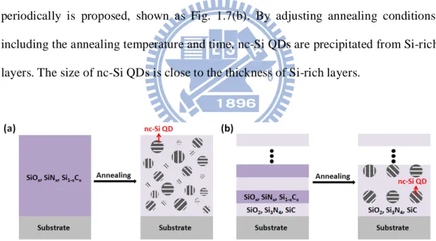
For Si precipitation from Si-rich layers, in order to form nc-Si QDs, high temperature annealing is necessary, shown as Fig. 1.7(a). In general, nc-Si QDs are embedded in the Si-based materials, such as SiO2, Si3N4, and SiC. The Si
precipitation mechanism can be expressed as [2,4]:
Si(O, N, C)x→ �x2� Si�O2, N4/3, C� + �1 −x2� Si. (2.4)
To control the size of silicon quantum dots more precisely, the multilayer structure stacked Si-based materials and their corresponding Si-rich layer (SiOx, Si1-xCx or SiNx)
periodically is proposed, shown as Fig. 1.7(b). By adjusting annealing conditions, including the annealing temperature and time, nc-Si QDs are precipitated from Si-rich layers. The size of nc-Si QDs is close to the thickness of Si-rich layers.
Fig. 1.7 The formation of nc-Si QDs in (a) a single Si-rich layer and (b) a multilayer structure.
The nc-Si QDs embedded in different materials with different bandgaps will affect the tunneling properties. Fig. 1.8 shows the energy band diagram of crystalline-silicon (c-Si) and its carbide, nitride and oxide [3,4,5]. Materials with smaller barrier height have higher tunneling probability and longer decay length. In order to overlap the
9
wave functions to produce electrical conductivity, the distance between nc-Si QDs embedded in different materials must be controlled effectively. For instance, dots in a SiO2 matrix have to be separated by no more than 1-2 nm, while they in a SiC matrix
are separated by more than 4nm [5].
Fig. 1.8 The energy band diagram of c-Si and its carbide, nitride and oxide [3,4,5]. X. J. Hao et al. fabricated nc-Si QDs in the SRO/SiO2 multilayer films by using the
sputtering method [12]. SRO layers with different O/Si ratio were grown by a co-sputtering technique. Increasing O/Si ratio caused Si QD size decrease and the absorption edge blue-shift, which was coincident with the quantum confinement. D. Song et al. prepared nc-Si QDs embedded in the SiC matrix by magnetron sputtering [11]. Different annealing temperatures effected the formation of Si and SiC nanocrystals. When the annealing temperature was higher (>800℃), the more SiC nanocrystals formed. T. W. Kim et al. reported nc-Si QDs embedded in silicon nitride by plasma-enhanced chemical vapor deposition (PECVD) using SiH4 and NH3 as
precursors [13]. The flow of SiH4 was fixed, while the flow of NH3 was varied.
Increasing the flow of NH3 caused the photoluminescence peak blue-shift and the
nc-Si QD size decrease.
10
QDs/p-type c-Si heterojunction device was 10.58% [14]. However, the conversion efficiency is lower than the theoretical calculation, because of a large power loss coming from low efficiency of carrier collection [3].
1.4.3 p-type ZnO thin films
For subsequent applications, the deposition of ZnO p-n homojunctions is needful. Due to the natural defects of oxygen vacancies and zinc interstitials, ZnO thin films generally show n-type conductivity [15,16,17]. It is difficult to obtain p-type ZnO. Therefore, researches in p-type ZnO have attracted a lot of attentions in recent years. Some studies have found acceptor dopants such as nitrogen (N), arsenic (As), and phosphorus (P) can cause ZnO to have p-type conductivity [15]. Compared with the deep acceptors of As and P, N is easier to contribute to p-type conductivity.
M. L. Tu et al. fabricated nitrogen-doped p-type ZnO (ZnO:N) using ZnO target by radio-frequency (RF) magnetron sputtering with an Ar sputtering gas mixed with various flow levels of N2 [15]. The undoped ZnO thin films was n-type but was
converted to p-type, when the N2 was flowed and the acceptor-type N dopant
entrapped into ZnO thin films. The type of conductivity was resolved by the ratio of N2(molecular):N(atomic). C. Wang et al. deposited ZnO:N using pure Zn target by
DC reactive magnetron sputtering [16]. The sputtering gas was the mixture of Ar-N2-O2. The structure and electrical properties of the films were influenced by the
post-annealing treatment and the ratio of N2-to-O2. M. Dutta et al. prepared Al-N
codoped p-type ZnO thin films on n-Si wafers by sol-gel fabrication [18]. The heterojunction showed a good rectifying I-V characteristic.
Otherwise, the working pressure and the annealing process are key points to the formation of p-type ZnO. D. K. Hwang et al. proposed phosphrous (P)-doped p-type
11
ZnO grown by radio-frequency magnetron sputtering [19]. The films were grown at working pressure in a range of 20 to 1 mTorr and annealed at 800 ℃ for 3 min under ambient nitrogen by rapid thermal annealing (RTA) process. The P-doped ZnO films grown at a low working pressure had high crystallinity and low native defects. The annealing process converted the as-grown P-doped ZnO films with a semi-insulating property into P-doped p-type ZnO films.
1.5 Motivation
Most groups studying nc-Si QD thin films usually fabricate nc-Si QDs in Si-based materials, such as SiO2, Si3N4, and SiC [3,4,5]. However, the results are still
substantially lower than the theoretical value. This can be attributed to the unfavorable material characteristics of these Si-based matrices, that is, they are not electrically conductive [2,5], which in turn limits the device performance.
We propose to use Al-doped ZnO (AZO) as the matrix material due to its many potential applications and unique features over other conventional wide bandgap semiconductors, e.g. high transparency, nice crystallinity, and easiness to control the electrical properties [7,8,9]. Hence, AZO is very suitable and has great potential to serve as the matrix for nc-Si QD thin films.
When the ZnO films are grown on silicon substrates, an amorphous silicon oxide thin layer is generated at the interface [20,21,22]. As the annealing temperature increases, the thickness of the silicon oxide layer at the interface increases [20,21]. Thick silicon oxide layer causes the electrical decline. Therefore, in order to improve the silicon oxide layer between the ZnO films and silicon substrates, we propose to deposit p-type ZnO materials to form ZnO p-n homojunctions, even to combine with nc-Si QD thin films.
12
Thus, the main purpose of this thesis is to investigate the characterization of the nc-Si QDs embedded in the AZO matrix and the p-type ZnO thin films.
13
Chapter 2 Fabrication Process and Analyzing
Method
In this chapter, we introduce the fabrication process of our samples and the equipments for sample analyzing.
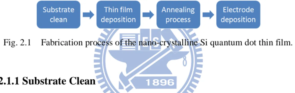
2.1 Fabrication Process
The fabrication process is shown in Fig. 2.1. We will describe all the details of each fabrication steps.
Fig. 2.1 Fabrication process of the nano-crystalline Si quantum dot thin film.
2.1.1 Substrate Clean
The beginning step as shown in Fig. 2.1 is substrate clean. We used p-type Si(100) wafers, n-type Si(100) wafers, quartzes, and wet oxide wafers as substrates.
The p-type and n-type Si wafers were cleaned by preliminary RCA clean to remove the native oxide layer. The steps of preliminary RCA clean are shown in Fig. 2.2. Finally, the wafers were dried in a flow of nitrogen.
14
Fig. 2.2 Preliminary RCA clean process of Si wafers.
The wet oxide films were deposited by the quartz furnace at 1050 ℃ for 3 hours on the Si wafers. The thickness of the wet oxide films was about 1 μm. We cleaned wet oxide wafers and quartzes ultrasonically with acetone and ethanol for 10 minutes to remove the organic contaminates. And then, the wafers were dried in a flow of nitrogen.
2.1.2 Thin Film Deposition
To analyze the characteristics of the undoped ZnO, Al-doped ZnO (AZO), and p-type ZnO thin films, we deposited single layer thin films. To analyze the characteristics of nano-crystalline silicon (nc-Si) quantum dot (QD) thin films, we deposited multilayer thin films. All of them were deposited by radio-frequency (RF) magnetron sputtering method.
For undoped ZnO and AZO thin films, we used two targets of pure ZnO and ZnO doped with 2 wt% Al2O3 and deposited them on p-type Si(100) wafers to form p-n
junctions, shown in Fig. 2.3(a) and (b). During deposition, argon (Ar) gas was chosen as the working gas, and the working pressure was kept at 5.0x10⁻³ Torr. The power of ZnO and AZO targets is fixed at 75 W. The thickness was about 100 nm. The
15
sputtering parameters in detail are shown in Table 2.1.
Fig. 2.3 The structure of (a) undoped p-type ZnO, (b) Al-doped ZnO, and (c) p-type ZnO thin films deposited on Si wafers.
Table 2.1 The sputtering parameters of undoped ZnO and AZO thin films.
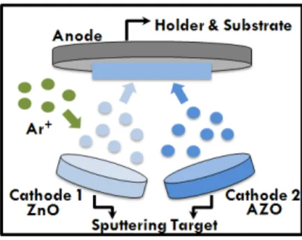
For the multilayer thin films, the targets of pure ZnO, ZnO doped with 2 wt% Al2O3, and Si were used. During deposition, Ar gas was chosen as the working gas,
and the working pressure was kept at 5.0x10⁻³ Torr. To tune the concentration of Al as matrix materials, we used the ZnO and AZO targets at the same time, and changed the power of them, shown in Fig. 2.4. We used the Si target to deposit amorphous Si and fixed the power at 110 W. The thicknesses of each AZO and Si layers were fixed at 5 nm and 3 nm, respectively. We deposited 20 pairs of AZO and Si layers and added 5 nm of AZO as a capping layer. Fig. 2.5 shows the structure of the multilayer thin films. Table 2.2 lists the sputtering parameters for different [AZO/Si]20 multilayer thin
films. The co-sputtering AZO samples, such as AZ5075 and AZ5025, are named by the power of the ZnO and AZO targets. For example, the sample AZ5075 means the ZnO sputtering power is 50 W and the AZO sputtering power is 75 W. In order to separate the multilayer structure from the single-layer structure, the names of [AZO/Si]20 multilayer thin films are added ML.
16
Fig. 2.4 Operation of sputtering during co-sputtering ZnO and AZO targets.
Fig. 2.5 The structure of the multilayer thin films.
Table 2.2 The sputtering parameters of the [AZO/Si]20 multilayer thin films.
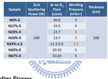
For the p-type ZnO thin films, we used the pure ZnO target and deposited them on n-type Si(100) wafers to form p-n junctions, shown in Fig. 2.3(c). High purity Ar and nitrogen (N2) gas were introduced into the chamber. We used the N2 as acceptor
dopants to contribute to p-type properties. During Deposition, the total gas flow was fixed at 30 sccm. The Ar-to-N2 flow was varied from 30:0 sccm to 10:20 sccm. The
17
pressure to 1.5x10⁻³ Torr. At this pressure, due to limitations of the sputtering machine, we changed the total gas flow to 15 sccm.All p-type ZnO sputtering power was fixed at 100 W. The thickness was about 200 nm. The sputtering parameters in detail are shown in Table 2.3. The samples are named by the ratio of the N2 and the
working pressure. For example, the sample named as N17%-5 means the ratio of the N2 is 17 % and the working pressure is 5 mTorr. In other words, the flow of the N2 is
7 sccm (30×17%=7).
Table 2.3 The sputtering parameters of p-type ZnO thin films.
2.1.3 Annealing Process
After deposition of the multilayer thin films, these samples were annealed by the quartz furnace in a N2 atmosphere to form nc-Si QD thin films. We fixed annealing
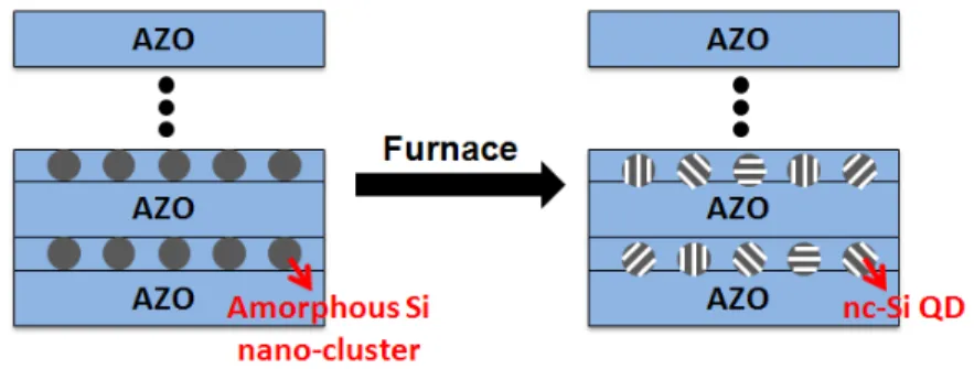
time at 5 minutes and changed annealing temperature between 700 to 1000 ℃. An illustration of the formation of nc-Si QDs in the AZO matrix is shown in Fig. 2.6.
18
Fig. 2.6 Illustration of the formation of nc-Si QDs embedded in the AZO matrix.
For the p-type ZnO thin films, we also annealed samples. We changed the annealing temperatures from 600 to 800 ℃ and times from 5 minutes to 1 hour in order to get p-type properties.
2.1.4 Electrode Deposition
Finally, contact electrodes were evaporated through the metal mask with 0.8 mm × 0.8 mm square pattern for the electrical properties measurement. For the p-type ZnO thin films, we deposited Ni electrodes (~120nm) on the top of samples and Al electrodes (~120nm) on the bottom of samples in order to reduce the influence of contact. For other samples, such as the undoped ZnO, AZO and multilayer thin films, opposite electrodes were deposited on the samples.
2.2 Analyzing Method
2.2.1 Four-Point Probe
Sheet resistance is one of the important characteristics to conductive materials. Four-point probe is the most commonly used tool to measure the sheet resistance. The current between the two probes is fixed, while the voltage difference between the other two probes is measured, then the sheet resistance can be calculated.
19
R = ρLA= ρWtL (2.1) where ρ is the resistivity, A is the cross-sectional area and L is the length. The cross-sectional area can be split into the width W and the thickness t. We can define the sheet resistance Rs as:
Rs =ρt (2.2)
Thus, the resistance can be rewritten as:
R = Rs L
W (2.3)
We use four-point probe (NAPSON, RT-80/RG-80) to measure the sheet resistance of thin films. And then, we check the thickness of thin films by N&K analyzer or alpha-step. Finally, we can understand the resistivity of the thin films from Eq. (2.2).
2.2.2 Current-Voltage Measurements
The current-voltage (I-V) curves were measured by using the E5270B 8-slot precision measurement mainframe (Agilent Technologies) and a halogen lamp was used for photo-response measurements. We can understand the formation of p-n junction between the thin films and the substrates by I-V characteristics.
In addition, we can use I-V characteristics to estimate the resistivity. The resistance is measured by the linear trend line of I-V characteristics. We can calculate the resistivity by combining the resistance with the eq. (2.1).
2.2.3 High Resolution X-Ray Diffractometer
X-ray diffractometer is a non-destructive analytical technique which reveals information about the crystallographic structure, chemical composition, and physical properties of materials and thin films. When x-ray irradiates crystalline materials,
20
constructive interference produces in some directions, determined by Bragg’s law:
2dsinθ = nλ
(2.5) where d is the spacing between diffracting planes, θ is the incident angle, n is any integer, and λ is the wavelength of the beam.
We can estimate the size of nc-Si QDs by using the Scherrer formula [12]:
R =Δ2θ(rad)∙cosθKλ (2.6) where L is the average nanocrystal size, λ is the x-ray wavelength, 2θ is the Bragg diffraction angle in radians, and K is a constant correction factor depending on the shape and size of the crystalline clusters, and on the direction of the diffracting planes. We analyzed our samples by high resolution x-ray diffractometer (Bede, D1) with θ-2θ mode. The wavelength of the x-ray was 1.54 Å.
For pure ZnO peaks, (002), (101) and (102), appear at 2θ = 34.68°, 36.46° and 47.50°, respectively [24]. For ZnO:N films, two peaks at 2θ = 34° and 43° are attributed to the zinc nitride (321) and (332), respectively [16]. For nc-Si QD thin films, three peaks at 2θ = 28.4°, 47.4° and 56.3° are attributable to Si(111), (220) and (311), respectively [12].
2.2.4 High Resolution Confocal Raman Microscope
Raman microscope is a technique used to study vibrational modes in a material. When the incident photons interact with the molecules, the electrons transit from the ground state to a virtual state. If the energy isn’t absorbed by the molecules, it is released through the scattering method. The released energy is the same as the energy of the incident photons, called Rayleigh scattering; otherwise, it is called Raman scattering [25]. Therefore, Raman microscope is a powerful and non-destructive technique to understand the physical and chemical properties of a material.
21
We analyzed our samples by high resolution confocal Raman microscope (HOROBA, Lab RAM HR), and used a 488 nm diode-pumped solid-state (DPSS) laser. Si wafers were used to calibrate the crystalline Si signal at 520 cm-1 before measuring our samples.
For bulk ZnO, the peak at ~439 cm-1 is E2(high) mode associated with oxygen
atoms and the one at ~591 cm-1 is E1(LO) mode [26]. For ZnO:N, the peak at 582
cm-1 is attributed to the A1 (LO) mode of ZnO:N [15,27]. The other four peaks with
frequencies of 275, 510, 643, and 856 cm-1 may be considered local vibrational modes which are related to nitrogen concentration in ZnO:N films. For nc-Si QD thin films, three peaks are generally detected, inclusive of the amorphous Si (a-Si) at ~480 cm-1, the nc-Si between 510 and 520 cm-1, and the intermediate mode from a-Si to nc-Si between 500 and 510 cm-1 [28].
2.2.5 UV/VIS/NIR Spectrophotometer
We used UV/VIS/NIR spectrophotometer (Japan, Hitachi U-4100) to measure the transmittance T and reflectance R of our thin films. We also can find the absorbance of our thin films by
Absorbance = 100 − T − R (%).
(2.7) Thus, we can understand the optical properties of the thin films.
Otherwise, we can use the transmittance and reflectance spectra to estimate the optical bandgaps of the thin films. The absorption coefficient α is evaluated from T and R according to the following relation [7,29]:
α = 1tln �1−RT � cm−1 (2.8)
where t is the thickness of the films. The optical bandgaps (Egopt) of the films are
22 relationship as [29]
(αhv)γ= B(hv − E
gopt) (2.9)
where h is Planck’s constant, v is the frequency of the radiation, and B is the edge width parameter. The value of γ is dependent on the Egopt behavior, such as γ=2 for
23
Chapter 3 Characterization of the nano-crystalline
Si quantum dots embedded in the Al-doped ZnO Thin
Films
Before analyzing the characterization of the nano-crystalline silicon (nc-Si) quantum dots (QDs) embedded in the Al-doped ZnO (AZO) thin films, we would like to know the characteristics of the AZO thin films and compare the properties with the ZnO thin films.
And then, we explored the nc-Si QDs embedded in AZO thin films from different annealing temperatures, different Al concentrations, and the comparison of the nc-Si QDs embedded in the ZnO and AZO matrix. We analyzed the characteristics by using Raman microscope, UV/VIS/NIR spectrophotometer, and current-voltage (I-V) characteristics. We can obtain the crystalline phase of Si for the nc-Si QD thin films by Raman spectrum. We can know the optical properties and estimate the optical bandgaps of the nc-Si QD thin films from UV/VIS/NIR spectrum. From I-V characteristics, we can understand the rectification characteristics and resistivity of the nc-Si QD thin films.
3.1 Characterization of the Al-doped ZnO Thin Films
We used the targets of pure ZnO and ZnO doped with 2 wt% Al2O3 to deposit the
ZnO and AZO thin films, and the target of ZnO doped with 2 wt% Al2O3 to deposit
AZO thin films. The sputtering parameters in detail are shown in Table 2.1.
From Hall measurements, the AZO and ZnO thin films show the n-type properties, which is resulting from the natural defects of oxygen vacancies and zinc interstitials [15].
24
The resistivity of the AZO and ZnO thin films annealed at 1000 ℃ for 5 minutes is 4.5×10⁻² and 1.3×10⁻¹Ω-cm. The resistivity decreases with the Al dopants. This can be caused by the replacement of Al3+ for Zn2+ [10].
Fig. 3.1(a) shows the transmittance of the AZO thin films annealed at 1000 ℃ for 5 minutes. The average transmittance of all the films is about 80% in the visible region. All the films have a sharp fall in the transmittance below 400nm because of the band edge absorption. The optical bandgaps of the AZO and ZnO thin films are determined by the eq. (2.9). Because ZnO is a direct bandgap material [30], the value of γ is 2. The curves (αhν)2 as a function of energy (hν) of the incident radiation is shown in Fig. 3.2(b). The inset shows the optical bandgaps of the AZO and ZnO thin films annealed at 1000 ℃ for 5 minutes. The widening of the optical band gap with Al dopants follows the Burstein-Moss effect [8].
Fig. 3.1 (a) Transmittance and (b) plots of (αhν)2 versus (hν) for the AZO and ZnO
thin films annealed at 1000 ℃ for 5 minutes. The inset in (b) shows the optical bandgaps of the samples.
The conductivity of the AZO thin films is better than the ZnO thin films. Thus, we want to embed the nc-Si QDs in the AZO thin films. We hope the conversion efficiency of the nc-Si QD solar cells increases by using the good conductive properties of the AZO thin films.
25
3.2 Influence of Different Annealing Temperatures
From now on, we start to discuss the nc-Si QDs embedded in the AZO thin films. The sputtering parameters in detail are shown in Table 2.2.
First, we explored the influence of different annealing temperatures on the nc-Si embedded in the AZO thin films. We focused on the sample AZ5075-ML to change the annealing temperatures from 700 to 1000 ℃ and fix the annealing time at 5 minutes.
Fig. 3.2 shows the Raman spectra of the sample AZ5075-ML annealed at different temperatures. As the annealing temperature increases, the silicon peak moves from the intermediate mode (500~510cm-1) to the nano-crystalline mode (510~520cm-1). This means a high annealing temperature is needed to form nc-Si QDs.
Fig. 3.2 Raman spectra of the sample AZ5075-ML annealed at different temperatures.
Fig. 3.3 shows the optical transmittance and absorbance spectra for the sample AZ5075-ML annealed at different temperatures. The transmittance increases with increasing the annealing temperature, while the absorbance decreases with increasing the annealing temperature. Changing in the transmittance is resulted from the better crystal quality of the AZO matrix after annealing at high temperatures [8,31]. In other
26
words, the better crystal quality of the AZO matrix after annealing means the reduction of defects, which cause the absorbance decreases.
Fig. 3.3 (a) Transmittance and (b) absorbance spectra of the sample AZ5075-ML annealed at different temperatures.
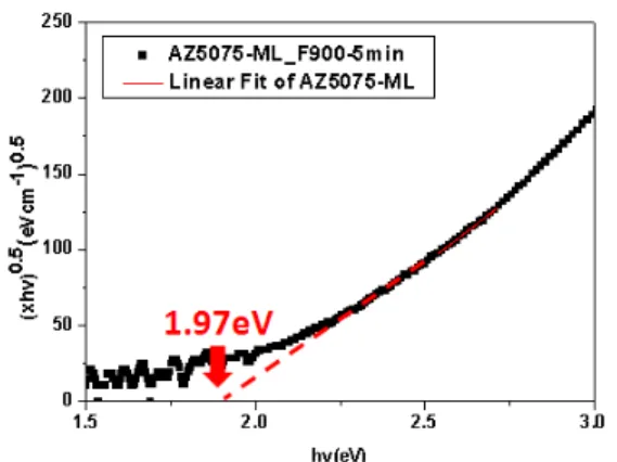
The optical bandgaps are determined by the eq. (2.9). The value of γ is 1/2 since a phonon-assisted transition dominates the optical processes for a small nc-Si QD size [29]. Here, we select the sample AZ5075-ML annealed at 900 ℃ for 5 minutes as a example for how to find the optical bandbap, shown in Fig. 3.4. The optical bandgap for the sample AZ5075-ML annealed at 900 and 1000 ℃ is 1.97 and 2.08 eV, respectively. The optical band gap increases with the increase of the annealing temperature, which means the decreases in nc-Si QD size [32].
Fig. 3.4 The example for how to find the optical bandbap. The sample is AZ5075-ML annealed at 900 ℃ for 5 minutes.
27
We changed different annealing temperatures to search an appropriate annealing temperature. The samples AZ5075-ML annealed at 900 and 1000 ℃ form the nc-Si QDs. The optical bandgap of the sample annealed at 1000 ℃ is wider than the sample annealed at 900 ℃, which means the decrease of the nc-Si QD size.
3.3 Influence of Different Al Concentrations
Here, we focus on the influence of different Al concentrations. All the [AZO/Si]20
thin films were annealed at 1000 ℃ for 5 minutes to form the nc-Si QDs in the AZO matrix. We use different powers of the AZO and ZnO targets to change the Al concentrations. In order to know the concentration of Al in the AZO thin films, we deposited the sample AZ75, AZ5075, and AZ5025 with the thickness of about 100nm and then measured these films by X-ray photoelectron spectroscopy (XPS), listed in Table 3.1. The Al concentration of the film deposited by a single AZO target is larger than the co-sputtering films. When the sputtering power of AZO is higher, the Al concentration of the films is larger.
Table 3.1 The concentration of atoms in the AZO thin films measured by XPS.
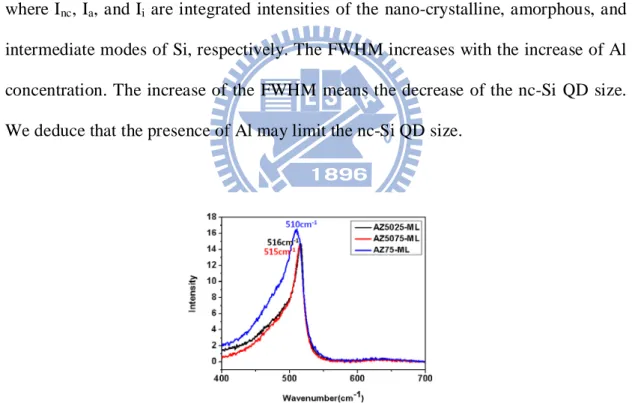
Fig. 3.5 shows the Raman spectra of the samples with different Al concentrations annealed at 1000 ℃ for 5 minutes. The peaks of all the samples are in the range of 510 to 520 cm-1, which represents the formation of nc-Si QDs in all the samples. In order to understand the individual contribution of the Raman signal, we fitted the Raman data of all the samples by using the program of PeakFit v4. Four peaks of the
28
E2(high) mode of ZnO at ~439 cm-1, the amorphous Si (a-Si) at ~480 cm-1, the
intermediate mode between 500 and 510 cm-1, and the nc-Si between 510 and 520 cm-1 were considered to fit the Raman data. The Raman spectrum and correspondingly fitting curve for the sample AZ5025-ML are shown in Fig. 3.6 as an example. Different ZnO and Si modes were considered in the best fit procedure, whose peak position, intensity area, full width at half maximum (FWHM) and crystallinity are recorded in Table 3.2. The crystallinity XC was determined from the
following equation [33]
XC =
Inc+Ii
Inc+Ii+Ia× 100%
(3.1)
where Inc, Ia, and Ii are integrated intensities of the nano-crystalline, amorphous, and
intermediate modes of Si, respectively. The FWHM increases with the increase of Al concentration. The increase of the FWHM means the decrease of the nc-Si QD size. We deduce that the presence of Al may limit the nc-Si QD size.
Fig. 3.5 Raman spectra of the samples with different Al concentrations annealed at 1000 ℃ for 5 minutes.
29
Fig. 3.6 Raman spectra and fitting curve for the sample AZ5025-ML annealed at 1000 ℃ for 5 minutes. The line (dash, red) is the Raman spectra, while the line
(solid, black) is the corresponding fit.
Table 3.2 The fitting results of the Raman curves for the samples AZ5025-ML, AZ5075-ML, and AZ75-ML annealed at 1000 ℃ for 5 minutes.
The crystallinity of the samples decreases with the increase of Al concentration, except the sample AZ5075-ML. X. J. Hao et al. investigated the effects of boron (B) concentration on Si QD/SiO2 multilayer films [34]. The addition of B suppresses Si
crystallinity. In this thesis, the role of Al is equivalent to the role of B, which act as dopants to improve the electrical properties. In other words, the decrease of the Si crystallinity is resulted from the suppression of Al. The exception of the sample AZ5075-ML will be discussed later.
Fig. 3.7 shows the transmittance spectra of the samples with different Al concentrations annealed at 1000 ℃ for 5 minutes . The transmittance decreases with the increase of the Al concentrations due to the free carrier absorption [8]. Then, we
30
estimated the optical bandgaps of the samples with different Al concentrations annealed at 1000 ℃ for 5 minutes. The optical bandgaps of the samples AZ5025-ML, AZ5075-ML, and AZ75-ML are 1.94, 2.08 and 2.15 eV, respectively. The widening of the optical band gaps with the increase of Al concentrations means the nc-Si QD size is narrower, which is corresponding to the trend of the FWHM from the Raman results.
Fig. 3.7 Transmittance spectra of the samples with different Al concentrations annealed at 1000 ℃ for 5 minutes.
Fig. 3.8 shows the I-V curves of the samples with different Al concentrations annealed at 1000 ℃ for 5 minutes. We find the samples AZ5025 -ML, AZ5075-ML and AZ75-ML show the rectification characteristics with the rectification values of 4.9×101, 1.5×10² and 4.0×10⁴ at ±2 V, respectively. We used the I-V curves to estimate the resistivity. The resistivity of the samples AZ5025-ML, AZ5075-ML and AZ75-ML is 9.0×10⁶, 4.3×10⁷, and 2.2×10⁶Ω-cm, respectively. In general, as the Al concentration increases, the conductivity decreases. However, the resistivity of the sample AZ5075-ML doesn’t show the trend. We suppose it is caused by the difference of the surface morphology. Thus, we check the surface morphology of the sputtering parameters of AZ5025, AZ5075, and AZ75 with the thickness of 5 nm by using atomic force microscopy (AFM), shown in Fig. 3.9. From the root mean square
31
(Rms) of the AFM images, the surfaces of the samples AZ5025 and AZ75 are flatter, while the sample AZ5075 is rougher. We also check the surface morphology of the multilayer thin films annealed at 1000 ℃ for 5 minutes by using scanning electron microscope (SEM), shown in Fig. 3.10. The multilayer thin films after annealing are bending. There are many convexes on the films. The density of the convexes is showed below the corresponding SEM images. The sample AZ5075-ML has the most convexes on the films, which is consistent with the AFM results. The rough surface can be used to explain why the poor conductivity and high crystallinity of the sample AZ5075 has.
Fig. 3.8 I-V curves of the samples with different Al concentrations annealed at 1000 ℃ for 5 minutes.
Fig. 3.9 AFM images of the as-deposited samples (a) AZ5025, (b) AZ5075, and (c) AZ75 with the thickness of 5 nm.
32
Fig. 3.10 SEM images of the samples (a) AZ5025-ML, (b) AZ5075-ML, and (c) AZ75-ML annealed at 1000 ℃ for 5 minutes.
Here, we identify the structural, optical and electrical properties of the nc-Si embedded in the AZO thin films are influenced by the Al concentrations. Increase in Al concentration can inhibit suppresses the nc-Si size and Si crystallinity. Moreover, the rougher surface morphology possibly causes the decrease of the conductivity and high Si crytallinity.
3.4 Comparison of the nc-Si QDs embedded in the ZnO and AZO
Thin Films
Confirmed the feasibility of the nc-Si QDs embedded in the AZO thin films, we want to compare the structure of [ZnO/Si]20 and [AZO/Si]20.
Fig. 3.11 shows the Raman spectra of the samples Z75-ML and AZ75-ML annealed at 1000 ℃ for 5 minutes. All the samples show the peak between 510 and
33
520 cm-1 which means the formation of the nc-Si QDs. The fitting results of the Raman spectra are recorded in Table 3.3. When Al is doped in the ZnO matrix, the FWHM is larger and the Si crytallinity is smaller, which coincides with the results in Section 3.3.
Fig. 3.11 Raman spectra of the samples Z75-ML and AZ75-ML annealed at 1000 ℃ for 5 minutes.
Table 3.3 The fitting results of the Raman spectra for the samples Z75-ML and AZ75-ML annealed at 1000 ℃ for 5 minutes.
Fig. 3.12 shows the absorbance spectra of the samples Z75-ML and AZ75-ML annealed at 1000 ℃ for 5 minutes. As Al is doped in the nc-Si QD thin films, the absorbance curve shows a blue-shift. The optical band gaps of the samples Z75-ML and AZ75-ML are 1.91 and 2.15 eV, respectively. This is corresponding to the result of the Raman data, which means the smaller size of the nc-Si QDs after doping Al. The smaller size of nc-Si QDs absorbs short wavelength light to verify the change of the absorbance spectra.
34
Fig. 3.12 Absorbance spectra of the samples Z75-ML and AZ75-ML annealed at 1000 ℃ for 5 minutes.
Fig. 3.13 shows the I-V curves of the samples Z75-ML and AZ75-ML annealed at 1000 ℃ for 5 minutes. Because Al acts as donors in the nc-Si QD thin films, the current is larger after doping Al. This phenomenon can also be found by the decrease of the resistivity. The resistivity of the samples Z75-ML and AZ75-ML is 6.0×10⁶ and 2.2×10⁶Ω-cm.
Fig. 3.13 I-V curves of the samples Z75-ML and AZ75-ML annealed at 1000 ℃ for 5 minutes.
We demonstrate the structure of the nc-Si QDs embedded in the AZO matrix. Doping Al in the nc-Si QD thin films limits the nc-Si QD size and Si crystallinity. The optical band gap and conductivity increase after doping Al.
35
3.5 Problems of the nc-Si QDs embedded in the Al-doped ZnO Thin
Films
In the analytic process of the nc-Si QDs embedded in the AZO thin films, we found there were some problems occurred in the films. Fig. 3.14 shows the SEM images of (a) the as-deposited AZ5025-ML and (b) the AZ5025-ML annealed at 1000 ℃ for 5 minutes. The as-deposited multilayer thin film is flat, but the multilayer thin film after annealing is bending. There are many gaps between the multilayer thin films and the Si substrates from the cross-sectional SEM images. The gap height is about 50 nm measured from the high-resolution SEM images, shown in Fig. 3.15. Other multilayer samples also have the bending problem after annealing. We suggest that the bending films are caused by the difference of the thermal expansion coefficient between the nc-Si QDs and ZnO matrix. During the annealing process, the release of thermal stress caused the bending multilayer thin film.
Fig. 3.14 SEM images of (a) the as-deposited sample AZ5025-ML and (b) the sample AZ5025-ML annealed at 1000 ℃ for 5 minutes.
36
Fig. 3.15 High-resolution SEM images of the sample AZ5075-ML annealed at 1000 ℃ for 5 minutes. (a) and (b) are any two points in the sample.
Fig. 3.16 shows the transmission electron microscopy (TEM) images of (a) the as-deposited Z75-ML and (b) the Z75-ML annealed at 1000 ℃ for 5 minutes. The bending problem can also be observed in the TEM images. Some gaps formed between the multilayer thin films and the Si substrates, shown in Fig. 3.16 (b). Otherwise, we can see the silicon oxide layer formed at the interface of multilayer thin films and the Si substrates by the high-resolution TEM images, shown in Fig. 3.17. A very thin (~2nm) silicon oxide layer formed before annealing, while the silicon oxide layer is thicker (~5nm) after annealing. It is emphasized that no silicon oxide interlayer was intentionally grown between the multilayer thin films and the Si substrates. This may be resulted from the reaction of oxygen atoms and Si surface [20].
37
Fig. 3.16 TEM images of (a) the as-deposited Z75-ML and (b) the Z75-ML annealed at 1000 ℃ for 5 minutes.
Fig. 3.17 High-resolution TEM images of (a) the as-deposited Z75-ML and (b) the Z75-ML annealed at 1000 ℃ for 5 minutes.
The problems of the bending films after annealing and the silicon oxide layer between the multilayer thin films and the Si substrates will largely decrease the device’s performance. Thus, we need to find ways to improve these problems.
In summary, we demonstrate the structure of the nc-Si QDs embedded in the AZO matrix. A high annealing temperature is needed to form the nc-Si QDs. As the Al concentration increase, the nc-Si QD size and Si crystallinity decrease, which means the suppression of Al. The conductivity of the nc-Si QD thin films increases with the increase of the Al concentration. However, the rougher surface morphology possibly causes the decrease of the conductivity. The silicon oxide layer between the multilayer thin films and the Si substrates and the bending films after annealing are
38
39
Chapter 4 Characterization of the p-type ZnO thin
films
In Section 3.5, we find the formation of silicon oxide layer between the Si substrates and [ZnO/Si]20 multilayer thin films. The thickness of the silicon oxide
layer is thicker after annealing. The silicon oxide layer at the interface may cause poorer electricity than we expected. Thus,we propose to deposit the p-type ZnO films to replace the Si substrates. When the substrates and the films are homogeneous materials, such as ZnO p-n homojunctions, the interface doesn’t exist silicon atoms to take oxygen away from ZnO and form silicon oxide layer. Therefore, ZnO p-n homojunctions can solve the problem of the interface silicon oxide layer.
Taking into account the feasibility of processing machine at hand, we used radio-frequency (RF) magnetron sputtering method through the nitrogen gas (N2) in
the manufacturing process to deposit p-type N-doped ZnO films. The sputtering parameters in detail are listed in Table 2.3. In addition to changing the sputtering parameters, we also changed the annealing conditions to get better features of the p-type ZnO films.
4.1 Analysis of High Resolution Confocal Raman Microscope
First, we wanted to examine whether the nitrogen atoms entrap into the ZnO thin films. Thus, we measured the ZnO thin films grown with mixture of argon (Ar) and N2 gas by Raman microscope, shown in Fig. 4.1. The inset shows the Raman spectra
of the ZnO thin films deposited with mixture of oxygen (O2) and N2 gas. Numbers in
the name represent the gas flow. For example, the sample O10N20 means the ZnO thin films grown with O2 of 10 sccm and N2 of 20 sccm. The sample N0%-5 is used
40
as a reference sample. Two peaks at 436.6 and 574.4 cm-1 shows in this sample, corresponding to E2(high) and E1(LO) mode of ZnO, respectively [26]. For other
samples N17%-5 to N67%-5, in addition to two peaks attributed to ZnO, there are other three peaks at 505.0, 637.8 and 849.6 cm-1, related to the local vibrational modes of N-doped ZnO (ZnO:N) [27]. Table 4.1 shows the N concentration in the ZnO:N thin films measured by X-ray photoelectron spectroscopy (XPS). We confirm again that N atoms were entrapped into the ZnO films.
Fig. 4.1 Raman spectra of the ZnO thin films grown with mixture of Ar and N2. The
inset shows the Raman spectra of the ZnO thin films grown with mixture of O2 and
N2.
Table 4.1 The concentration of Zn, O and N atoms in the ZnO:N thin films measured by XPS.
41
For the ZnO samples grown with mixture of O2 and N2, such as O10N20 and
O20N10, two peaks are all contribution of ZnO. There are no peaks related to ZnO:N, which means the N atoms don’t entrap into the ZnO thin films. This can be attributed to the preferential combination of Zn with O rather than with N, because the chemical activity of O is higher than that of N [35].
Therefore, we confirm that the ZnO:N thin films can be deposited in the manufacturing process with mixture of Ar and N2. However, whether the electrical
properties of the ZnO:N thin films are p-type must be investigated by current-voltage (I-V) characteristics.
4.2 Analysis of Current-Voltage Characteristics
Here, we deposited the ZnO:N thin films on n-type Si substrates to form p-n junctions and investigated the electrical properties by I-V characteristics. Fig. 4.2 shows the I-V curves of the ZnO:N thin films with different N2 flow. The samples in
the Fig. 4.2(a) were as-deposited, while the samples in the Fig. 4.2(b) were annealed at 600 ℃ for 5 minutes. All the as-deposited samples don’t show the rectification characteristics. The annealed samples are with the rectification characteristics, but still not p-type properties. Thus, we tried to change working pressure during the deposition of the ZnO:N thin films.
42
Fig. 4.2 I-V curves of the ZnO:N thin films with different N2 flow (a) before and (b)
after annealing at 600 ℃ for 5 minutes.
The N (atomic) is a p-type dopant and N2 (molecular) is a n-type dopant to the
ZnO films [36]. Higher N2 flow rates limit the ionization of N2. In order to deposit the
p-type ZnO:N thin films, the ratio of N2(molecular):N(atomic) is a critical factor.
Therefore, we chose the samples with N2 flow of 23% to change the working pressure.
Fig. 4.3 shows the I-V curves of the ZnO:N thin films with N2 flow of 23% deposited
at different working pressure. The samples in the Fig. 4.3(a) were as-deposited, while the samples in the Fig. 4.3(b) were annealed at 600 ℃ for 5 minutes. All the as-deposited samples don’t show the rectification characteristics. After annealing, the ZnO:N thin films deposited at low working pressure, such as the samples N23%-3 and N23%-1.5, show the p-type rectification characteristics with the rectification values of 90 and 13 at ±3 V, respectively. The carrier type of the samples N23%-3 and N23%-1.5 annealed at 600 ℃ were examined by Hall measurements. The result shows the two samples are indeed p-type properties.
43
Fig. 4.3 I-V curves of the ZnO:N thin films with N2 flow of 23% deposited at
different working pressure (a) before and (b) after annealing at 600 ℃ for 5 minutes.
Thus, a thermal activation mechanism occurred for these nitrogen acceptors [15], and the samples N23%-3 and N23%-1.5 annealed at 600 ℃ show p-type properties. Compared with the samples with N2 flow of 23%, such as N23%-5, N23%-3, and
N23%-1.5, the samples deposited at low working pressure show p-type properties. This can be supposed the ZnO:N thin films deposited at low working pressure show high crystal quality or reduce structural defects, or native defects [19]. From the X-ray diffractometer (XRD) results, shown in Fig. 4.4, the sample N23%-3 annealed at 600 ℃ for 5 minutes show the peaks corresponded to ZnO (002), (101), and (103). Because of low N concentration, shown in Table 4.1, the sample N23%-3 after annealing has good crystal quality. The ZnO:N thin films deposited at low working pressure indeed have better crystal quality.
44
Fig. 4.4 XRD spectra of the samples N23%-5 and N23%-3 annealed at 600 ℃ for 5 minutes.
Next, we changed different annealing conditions for the sample N23%-3, inclusive of temperatures and times. We wanted to adjust better annealing parameters. Fig. 4.5 shows the I-V curves of the sample N23%-3 annealed at different conditions. The samples annealed at 600 ℃ for 5 and 10 minutes show the p-type rectification characteristics, while other annealing conditions (higher temperature and longer time) shows no p-type rectification characteristics. Thus, appropriate annealing temperature and time can cause the activation of N acceptors. Higher temperature and longer time drive N acceptors to inactive forms.
Fig. 4.5 I-V curves of the sample N23%-3 annealed at different conditions. (a) shows the influence of annealing temperatures, while (b) shows the influence of
45
Consequently, the p-type ZnO thin films can be grown by adjusting the sputtering parameters and annealing conditions. The ZnO:N thin films can be deposited by using the sputtering method with mixture of Ar and N2. By reducing the working pressure
during the sputtering process to get better crystal quality and annealing to activate N acceptors, the p-type ZnO:N thin films can be fabricated.
4.3 Analysis of ZnO p-n Homojunctions
In Section 4.2, we can use the sputtering parameters and annealing conditions to deposit p-type ZnO:N thin films. Here, we integrate the p-type ZnO:N thin films with the n-type ZnO thin films to form ZnO p-n homojunctions.
We used wet oxide wafers as substrates. First, we deposited Ni electrodes (~120nm) on the substrates by the thermal coater. Second, we deposited p-type ZnO:N thin films (~200nm) and n-type ZnO thin films (~200nm) in sequence by the sputtering method. Third, we annealed the sample at 600 ℃ for 5 minutes to activate the N acceptors by the furnace. Finally, we deposited Al electrodes (~120nm) on the sample by the thermal coater. The structure of the ZnO p-n homojunction and detailed processing parameters are showed in Fig. 4.6.
Fig. 4.6 The structure of the ZnO p-n homojunction. The detailed processing parameters also list next to the corresponding layer.
![Fig. 1.1 Changes in global warming (blue, left-hand scale) and fossil fuel consumption (red, right-hand scale) with time [1]](https://thumb-ap.123doks.com/thumbv2/9libinfo/8342427.176107/12.893.203.614.528.822/changes-global-warming-scale-fossil-consumption-right-scale.webp)
![Fig. 1.6 Schematic of (a) two-cell and (b) three-cell tandem solar cell [4].](https://thumb-ap.123doks.com/thumbv2/9libinfo/8342427.176107/17.893.241.669.794.1045/fig-schematic-cell-b-cell-tandem-solar-cell.webp)

![HPSH [ 氧化數平衡反應式係數 ]](data:image/gif;base64,R0lGODlhAQABAIAAAP///wAAACH5BAEAAAAALAAAAAABAAEAAAICRAEAOw==)