國立臺灣大學工學院材料科學與工程學系 博士論文
Department of Materials Science and Engineering College of Engineering
National Taiwan University Doctoral Thesis
3D IC 封裝中接點空間受限誘發之界面反應關鍵效應
Critical Issues in Soldering Reactions Arising from Space Confinement in 3D IC Packages
莊鑫毅 Hsin-Yi Chuang
指導教授:高振宏 博士 Advisor: C. Robert Kao, Ph.D.
中華民國 101 年 1 月 January, 2012
I
ACKNOWLEDGEMENT
The author would like to express his sincere gratitude to his advisor, Professor C.
Robert Kao, for his patience, inspiration and guidance in advising him on the researches.
Also, he is grateful to Professor S. W. Chen, Dr. D. Y. Shih, Professor Albert Wu, Professor Y. W. Yen and Dr. T. C. Chang for their suggestions on generating this thesis.
Their valuable comments definitely improve the quality of the thesis. He also appreciates Professor J. M. Song and T. Y. Yang for bringing him into the interesting field of materials science.
The author would also like to give thanks to his colleagues and friends for their help, encouragement and friendship. In addition, he intends to thank God for leading him on the right path to confront with all challenges which have enriched his life.
Finally, the author is grateful to his lovely family for their unlimited love and supports.
Without them, he would not be able to attentively concentrate on his studies.
Hsin-Yi Chuang
Department of Materials and Engineering National Taiwan University
January, 2011
II
致 謝
本論文得以順利完成首要感謝指導教授高振宏博士在研究歷程與論文撰寫過 程中的悉心指導與幫助。同時也感謝陳信文教授、史達元博士、吳子嘉教授、顏 怡文教授、張道智博士參與研究討論並提出建議,這些建議也使得論文更趨完整。
一併感謝宋振銘教授與楊子毅教授過去的提攜與指教,是您們啟發了我走進材料 科學的大門,讓我置身其中獲得無限樂趣。
我衷心感謝棨睿、育蔚、彥良、明諺在我初來乍到時給了我莫大的幫助,讓 我能夠更快速地融入 ACPL 這個大家庭。也感謝素純、智強、儀雯、俊成、智峰、
珮萱和我一起渡過精實的修課時光。此外更要感謝這兩年和我一起在實驗上打拼 的伙伴們:楣詩、人睿、孟歆、玟伶、澄傑、挺立,有幸得與各位合作是我莫大 的殊榮,我由衷感激。謝謝佳宏、郁仁、偉銘不厭其煩的參與討論並給予指教,
令我受益良多。感謝景堯在實驗上的鼎力協助,也謝謝子軒、致帆、依樺、珈源、
冠育、挺嘉、炫達、子企、彥甫等所有實驗室的同學們,有了您們使得這些年的
研究生活添了許多色彩。感謝這四年來一路相挺的好朋友們:勻祺、明珠、瑪琍、
Renew 的朋友們、昌祺、禧鐘、承育、佑霖,以及所有曾經關心或幫助過我長輩與 朋友,在此一併致謝。最後,感謝上帝帶領我經歷了這一切的人、事、物,使我 的人生豐富精彩。
謹以此文獻給我親愛的家人:爺爺、奶奶、爸爸、媽媽、乾媽,感謝您們無 限的愛與包容,讓我能夠無後顧之憂的完成學業。您們的支持永遠是我向前邁進 的動力。
莊鑫毅 謹誌於
臺灣大學 材料科學與工程系 中華民國一零一年一月
III
ABSTRACT
Imminent ending of Moore’s law is the most critical issue threatening the continuing development of semiconductor industry. The strategy of consensus in order to go beyond Moore’s law is through the Three-Dimensional Integrated Circuit (3D IC) architecture.
Among many 3D IC integration schemes under development today, solder micro-bumping is a very promising one. Due to the extremely small size of solder joints in 3D IC packages, interfacial reaction features are quite different to that in the conventional solder joints. The space confinement behaviour must be considered in the soldering reactions. In this thesis, six critical issues in soldering reactions arising from space confinement are proposed and discussed. The first issue arises from the concern that intermetallics (IMCs) may occupy a large portion of the solder joint volume. It is demonstrated that this concern is not only for Cu substrate but also for Ni under bump metallurgy which reacts very slowly with solders. The second issue relates to impingement and merging of IMC grains. When IMCs occupy a large portion of a joint, the IMC grains growing from the opposite sides of a joint will eventually impinge on each other. The grains originally with different orientations can merge into a single grain after the impingement. Grain coarsening is considered to be a key reason responsible for the merging behaviour. The third issue is about the solder volume effects on the IMC
IV
growth rate. It is demonstrated that solder volume has very little effects on the IMC species and their growth rates. The fourth issue is relating to effects of inert alloy constituents, i.e., Ag and Bi, in the space confined soldering reaction. The inert phase will be rejected from the interfacial reaction, and eventually locates near the centre of the joint as the solder is fully consumed. Experimental results also reveal that the inert phase can form as a continuous layer throughout the joint as the solder originally contains a higher inert constituent content. This morphology is considered having a great impact on the joint strength. The fifth issue arises from the fact that as size of joint becomes smaller, the surface area-to-volume ratio increases. This makes the impact of thin film layers on UBM and surface finish become ever higher. One well known example is Au. The so-called Au embrittlement issue may become relevant again in the 3D IC packaging. The upper limit of Au content for preventing Au embrittlement is estimated to be 1.3 wt.% in Sn. The last issue is the volume shrinkage during soldering reactions. It is the first time that the reaction induced volume shrinkage is experimentally measured in a Ni-Sn soldering reaction. Internal stress or structure defects may form because of this shrinkage. Theoretical analysis and experimental evidence are presented in this thesis to illustrate these issues, and implications based on the findings will be also discussed.
V
Keywords: 3D IC, soldering reaction, space confinement, microstructure, IMC
growth, inert phase, Au embrittlement, volume shrinkage.
VI
摘 要
近年來半導體產業的發展逐漸落後於莫爾定律的預期,透過發展 3D IC 技術 以持續提供半導體產業發展的動能儼然成為各界共識。在眾多發展中的 3D IC 封 裝技術中,具微小銲料凸塊之晶片接合法是相當受到矚目的構裝方式。然而 3D IC 元件內之銲點尺寸非常微小,因此接點空間受限(Space confinement)所導致的 界面反應特徵勢必與傳統銲點不同。本研究基於理論分析與實驗結果提出計六項 因空間限制誘發之界面反應行為及其效應。第一項是 3D IC 接點中勢必存在大量 介金屬化合物,即便採用具有 Ni 層之表面處理層依舊如是。第二項效應為界面反 應發生時,來自對向之介金屬化合物會相互碰撞。此些原本具有不同結晶取向
(Grain orientation)之晶粒於碰撞後會逐漸密合為單一晶粒。研究中推測晶粒 粗化(Grain coarsening)是造成密合現象的重要因素。其三,實驗結果指出:
銲料體積減少對於介金屬之種類及成長速率並沒有顯著效應。其四,銲料中之鈍 態添加元素(Inert constituent)對於接點顯微結構具有顯著之影響。實驗中發 現 Ag 與 Bi 等鈍態添加元素會被阻絕於接點界面反應之外。換言之,鈍態相(Inert phase)會被排出並堆積於接點中央。當使用含有較高鈍態元素濃度之銲料時,這 些鈍態相甚至將於接點中央形成一連續層。此顯微組織極可能對接點強度造成不 良影響。其五,當銲料體積減少時,銲料層之表-體積比(surface area-to-volume ratio)將隨之上升。此時接點表面處理層之效應將大幅提升。其中最重要的影響
便是金脆效應(Au embrittlement)。實驗結果顯示當接點之 Au 濃度超過 1.3 wt.%
時,接點內將出現大量盤狀或層狀之(Au,Ni)Sn4,該顯微結構將導致接點強度劣化。
第六點為界面反應誘發之接點體積收縮效應。本研究係首次以完整的實驗結果證 明該效應的存在。接點中之體積收縮將可能誘發接點內應力以及結構缺陷,對接 點強度將具有相當大的影響。本文中除了呈現分析結果與實驗數據外,亦將針對 各效應可能衍生之可靠度議題進行探討。
VII
關鍵詞: 3D IC、銲接反應、接點空間限制、顯微結構、介金屬成長、頓態相、金 脆效應、體積收縮。
VIII
TABLE OF CONTENTS
ACKNOWLEDGEMENT ... I ABSTRACT ... III TABLE OF CONTENTS ... VIII LIST OF TABLES ... X LIST OF FIGURES ... XI
1.0 INTRODUCTION ... 1
1.1 Background Introduction ... 1
1.2 Definition and Causes of Space Confinement Behaviour ... 6
1.3 Issues Arising from Space confined Interfacial Reactions ... 8
1.3.1 Issue I: Peculiar Microstructural Features Attributed to Space Confinement ... 8
1.3.2 Issue II: Impingement and Merging of IMC Grains... 11
1.3.3 Issue III: Effects of Solder Volume Reduction on the IMC Growth Kinetics .. 15
1.3.4 Issue IV: Rise of Inert Alloy Constituent Concentration Due to Solder Consumption ... 16
1.3.5 Issue V: Area-to-volume Ratio Effect Relating to the Surface Finish .... 18
1.3.6 Issue VI: Soldering Reaction Induced Volume Shrinkage ... 20
1.4 Aims of the Thesis ... 24
2.0 EXPERIMENTAL DETAILS ... 25
2.1 Sample Preparation and Experimental Procedure ... 25
2.2 Theories and Assumptions for Kinetics Analysis ... 29
2.3 Alpha-step measurement ... 31
IX
3.0 RESULTS AND DISCUSSION ... 33
3.1 Peculiar Morphology of Cu/Sn/Cu and Ni/Sn/Ni Reactions ... 33
3.2 Impingement and Merging Behaviour of IMC Grains ... 43
3.3 Effects of Solder Volume Reduction on IMC Growth Kinetics ... 48
3.4 Effects of Inert Alloy Constituents in the Space Confined Soldering Reaction 59 3.4.1 Effects of Ag Addition: Formation and Re-distribution of Ag3Sn ... 59
3.3.2 Effects of Bi Addition: Formation and Re-distribution of Bi ... 70
3.5 Area-to-volume Ratio Effects Relating to the Surface Finish ... 78
3.6 Soldering Reaction Induced Volume Shrinkage ... 85
4.0 CONCLUSIONS AND IMPLICATIONS ... 89
REFERENCES ... 95
CURRICULUM VITAE ... 103
X
LIST OF TABLES
Table 1.1 Comparison of wire bonding and micro-bumping for achieving 3D IC. (Data collected from [3]) ... 4 Table 1.2 Theoretical molar volume values of common phases in soldering reactions.
(data obtained from [40, 41]). ... 22 Table 1.3 Calculated volume shrinkage ratios in typical Cu-Sn and Ni-Sn reactions. ... 22 Table 3.1 The k values of CuSn IMC growth at 250 oC. (Literature data are collected
from [49-51]) ... 50 Table 3.2 The k values of CuSn IMC growth at 150 oC. (Literature data are collected
from [46, 47, 52]) ... 50 Table 3.3 The k values of Ni3Sn4 growth at 250 oC. (Literature data are collected from [53, 54]) ... 54 Table 3.4 The k values of Ni3Sn4 growth at 150 oC. (Literature data are collected from [55-58]) ... 54 Table 3.5 The k values of Ni3Sn4 growth at 180 oC. (Literature data are collected from [59-61]) ... 54 Table 3.6 The k values of Ni3Sn4 growth at 200 oC. (Literature data are collected from [58-61]) ... 55 Table 3.7 Comparative study of apparent activation energies for Ni3Sn4 formation ... 55
XI
LIST OF FIGURES
Figure 1.1 Schematic drawings showing the concept of 3D IC. ... 2
Figure 1.2 Typical schemes for establishing 3D IC. (pictures taken from [2]). ... 3
Figure 1.3 3D IC through soldering bonding. (Photos taken from [10, 18]) ... 5
Figure 1.4 Solder volumes in different packaging levels. (Picture taken from [4]) ... 5
Figure 1.5 Micrographs showing the typical morphology of (a) 3D IC and (b) flip-chip joint. (Photos provided by ITRI and J. H. Ke) ... 7
Figure 1.6 Microstructure evolution of Cu/Sn(25m)/Cu sandwiches reacted at 340 oC for (a) 10, (b) 40, (c) 90 and (d) 480 min. (Photos taken from [6]) ... 10
Figure 1.7 Focused-ion-beam images showing the microstructure evolution of Cu/Sn (25m)/Cu sandwiches reacted at: (a) 260 oC for 5 min, (b) 300 oC for 10 min, (c) 300 oC for 480 min and (d) 340 oC for 480 min. (Photos taken from [6]) ... 14
Figure 1.8 An example of the crystal orientation map and the colour coding of IMC grains. (Photo taken from [19]) ... 14
Figure 1.9 Schematic drawing showing (a) the inert constituent randomly dispersing in the solder region and (b) the inert constituent is rejected and pushed toward the centre of the interface. ... 17
Figure 1.10 The schematic drawing indicating parameters in Equation 1.2 ~ 1.4. ... 19
Figure 1.11 The schematic drawing showing the volume shrinkage issue. ... 22
Figure 2.1 Schematic drawings showing two types of sandwiches prepared by electroplating and hot-pressing bonding. ... 27
Figure 2.2 Schematic drawings showing the type I sample preparation via electroplating. ... 27
XII
Figure 2.3 Schematic drawings showing the type II sample preparation via hot-pressing bonding. ... 27 Figure 2.4 The experimental setup of the alpha-step measurement. ... 32 Figure 3.1 Micrographs showing the Cu/Sn(10m)/Cu reaction at 250 oC for (a) 1, (b) 12, (c) 15 and (d) 20 min. ... 36 Figure 3.2 Micrographs showing the Cu/Sn(10m)/Cu bonded at 250 oC and then aged at 150 oC for (a) 144, (b) 240 and (c) 480 h. ... 37 Figure 3.3 Micrographs showing the Ni/Sn(10m)/Ni reaction at 250 oC for (a) 1, (b) 10, (c) 20, (d) 30, (e) 90 and (f) 180 min. ... 39 Figure 3.4 Micrographs showing the Ni/Sn(10m)/Ni aged at 180 oC for (a) 72, (b) 192 and (c) 240 h. The surface showed in (c) was prepared by using an ion beam polisher. ... 41 Figure 3.5 Scanning electron micrographs showing the Cu/Sn(15m)/Cu reactions at 250
OC for (a) 10, (c) 15 and (e) 20 min. (b), (c) and (f) are EBSD orientation maps corresponding to (a), (c) and (e), respectively. ... 45 Figure 3.6 Scanning electron micrographs (a) and the EBSD orientation map (b) showing Cu/Sn(15m)/Cu reactions at 150 OC for 648 h. ... 45 Figure 3.7 Scanning electron micrographs (a) and (c), and EBSD orientation maps (b) and (e) showing the Ni/Sn(10m)/Ni reactions at 250 OC for 90 and 180 min. . 47 Figure 3.8 Averaged thickness of CuSn IMCs per interface at 250 oC. Symbol Ο denotes data point for Cu/Sn(10m)/Cu sandwiches. The The black line is fitted with the experimental data, and the grey lines are fitted from the literature data [49-51]. ... 50 Figure 3.9 Averaged thickness of CuSn IMCs per interface at 150 oC. Symbol Ο denotes data point for Cu/Sn(10m)/Cu sandwiches. The black line is fitted with the
XIII
experimental data, and the grey lines are fitted from the literature data [46, 47, 52]. ... 51 Figure 3.10 Averaged thickness of Ni3Sn4 per interface at 250 oC. Symbol Ο denotes data point for Ni/Sn(10m)/Ni sandwiches. The black line is fitted with the experimental data, and the grey lines are fitted from the literature data [53, 54]. ... 56 Figure 3.11 Averaged thickness of Ni3Sn4 per interface at 150, 180, and 200 oC for
Ni/Sn(5 m)/Ni and Ni/Sn(10m)/Ni sandwiches. Solid symbols (▲, ■, ●) denote data points from Ni/Sn(5m)/Ni sandwiches. Hollow symbols ( , □,
○) denote data points from Ni/Sn(10 m)/Ni sandwiches. ... 56 Figure 3.12 Averaged thickness of Ni3Sn4 per interface at 150 oC. Solid symbol ● denotes data point from Ni/Sn(10m)/Ni sandwiches. Hollow symbol ○ denotes data points for Ni/Sn(10m)/Ni sandwiches. The black line is fitted with the experimental data, and the grey lines are fitted from the literature data [55-58]. ... 57 Figure 3.13 Averaged thickness of Ni3Sn4 per interface at 180 oC. Solid symbol ● denotes data point from Ni/Sn(10m)/Ni sandwiches. Hollow symbol ○ denotes data points for Ni/Sn(10m)/Ni sandwiches. The black line is fitted with the experimental data, and the grey lines are fitted from the literature data [59-61]. ... 57 Figure 3.14 Averaged thickness of Ni3Sn4 per interface at 200 oC. Solid symbol ● denotes data point from Ni/Sn(10m)/Ni sandwiches. Hollow symbol ○ denotes data points for Ni/Sn(10m)/Ni sandwiches. The black line is fitted with the experimental data, and the grey lines are fitted from the literature data [58-61]
... 58
XIV
Figure 3.15 Arrhenius plot for the formation of Ni3Sn4 in Ni/Sn(5m)/Ni and Ni/Sn(10m)/Ni sandwiches. ... 58 Figure 3.16 (a)-(d) Micrographs showing the Ni/Sn(7m)/Ni sandwiches after aging at 180 oC for (a) 28, (b) 48, (c) 120, and (d) 240 h. The cross-sections in (a)-(c) were prepared by mechanical polishing, and that in (d) was prepared by using an ion beam cross-section polisher. (e) Micrograph from a Ni/Sn(5m) bi-layer structure that had its Sn completely been consumed. No void was observed because now the volume shrinkage due to reaction was completely compensated by thickness decrease. ... 62 Figure 3.17 Schematic drawings showing the sequences of the void formation. (a) The stage before IMC impingement. (b) Shows the impingement occurs at certain places. (d) Sn is already consumed leaving a few voids in the joint. ... 64 Figure 3.18 Micrographs showing the Ni/Sn2.4Ag(7m)/Ni sandwiches after aging at
180 oC for (a) 12, (b) 72, (c) 378 and, (d) 528 h... 67 Figure 3.19 Averaged thickness of Ni3Sn4 per interface at 150, 180, and 200 oC. Symbols , ▼, ▲ and □ represent data points for Ni/Sn(5m)/Ni, Ni/Sn(7m)/Ni, Ni/Sn(10m)/Ni, and Ni/Sn2.4Ag(7m)/Ni, respectively. ... 69 Figure 3.20 Micrographs showing the Cu/Sn10Bi(10m)/Cu sandwiches bonded at 250
oC and then aged at 120 oC for (a) 150, (b) 600, (c) 750, (d) 900 and (e) 1050 h. ... 75 Figure3.21Micrographs showing the Cu/Sn10Bi(10m)/Cu sandwiches in the (a)
as-bonded condition at 250 oC, and after aging at 120 oC for (b) 96, (c) 300 and (c) 450 h. ... 76 Figure 3.22 Schematic drawings showing the impurities become concentrated as more
and more solder is converted into IMC. (a) As-assembly condition. (b)
XV
Two-third of the solder consumed, and (c) All solder been consumed. ... 77 Figure 3.23 Micrographs showing the Ni/Sn0.8Au(10m)/Ni sandwiches in the (a) as
bonded condition at 250 oC, and after aging at 200 oC for (b) 48, (c) 72 and (d) 96 h. ... 79 Figure 3.24 Micrographs showing the Ni/Sn1.3Au(10m)/Ni sandwiches in the (a) as
bonded condition at 250 oC, and after aging at 200 oC for (b) 24, (c) 72 and (d) 168 h. ... 81 Figure 3.25 Micrographs showing the Ni/Sn2.6Au(10m)/Ni sandwiches in the (a) as
bonded condition at 250 oC, and after aging at 200 oC for (b) 48, (c) 96 and (d) 144 h. ... 82 Figure 3.26 Micrographs showing the Ni/Sn3.9Au(10m)/Ni sandwiches in the (a) as
bonded condition at 250 oC, and after aging at 200 oC for (b) 72 and (c) 96 h.
... 83 Figure 3.27 The surface profile of Ni/Sn(5m)/Ni changing with aging time. ... 87 Figure3.28 Micrographs showing the Ni/Sn(5m)/Ni sandwiches in the (a) as-plated
condition, and after aging at 180 oC for (b) 8, (c) 16, (d) 24 and (e) 168 h.88
1
1.0 INTRODUCTION
1.1 Background Introduction
Imminent ending of Moore’s law is the most critical issue threatening the continuing development of semiconductor industry. The Moore’s law states that the number of transistors inside an integrated circuit doubles every 18 months. For the past 60 years, Moore’s law has been a key roadmap guiding the advancement of the semiconductor industry. As the shrinking of the critical dimension in integrated circuit becomes increasingly more difficult, semiconductor industry has to resort to other approaches achieving the goal of building ever smaller devices that consume less power and have higher performance. To this end, the three-dimensional integrated circuit (3D IC) architecture is favoured by most major semiconductor companies, including Intel, IBM, ARM, tsmc, and Samsung. As schematically showed in Figure 1, the 3D IC is a functional chip in which two or more layers of active electronic components are integrated vertically into a single circuit. The 3D IC has benefits such as higher performance, lower power requirement and smaller size than the conventional 2D IC.
2
Figure 1.1 Schematic drawings showing the concept of 3D IC.
Two typical 3D IC architectures achieved by wire bonding and solder micro-bumping are illustrated in Figure 1.2. Wire binding is a conventional approach producing 3D IC, in which Cu or Au wires connect the individual dies in a stack. In general, connections between chips go through the board or chip and back to other chips in the stack; however, it is also possible to bond from chip to chip in the stack. Wire bonding is a heating and mechanical vibrating assisted process, so that improper bonding parameters would cause tearing of the pad and perhaps destroy devices underneath the pad. In addition, this approach is limited by the resolution of wire bonders, and becomes increasingly difficult as the number of I/Os in the chip stack increases. Wire-bonds in package are possible only on the chip's periphery, which severely limits the interconnect density.
Compared to the wire bonding, solder micro-bumping is a much promising approach. This approach used an intermediate material such the solder on the surface of the die to make connections. Bumps in such a configuration typically have a height of several microns. The mechanical stresses arisen from assembly are much lower than
3
that from the wire bonding. The solder micro-bumping technology involves embedding previously fabricated die into a set of carrier wafers with a fixed size, enabling engineers to assemble them into a tight cube. This approach offers a much greater vertical interconnect density than the wire-bonding approach. Solder micro-bumping also enables the use of one or more chips, from the same or from different fabrication technologies, in each layer of the stack [1-3]. Solder micro-bumping can be even improved with the through silicon via (TSV) technology on power efficiency, IO density, heat dissipation and signal transmission. Pro and con of the 3D IC architecture accomplished by wire bonding and solder micro-bumping with TSV can be seen in Table 1.1.
Figure 1.2 Typical schemes for establishing 3D IC. (pictures taken from [2]).
4
Table 1.1 Comparison of wire bonding and micro-bumping for achieving 3D IC.
(Data collected from [3])
Solder micro-bumping is a very promising approach enabling 3D IC integration [4-9]. In fact, many researchers consider that as a very critical step for the entire 3D IC architecture [3, 10-17]. A good example of a 3D IC through this approach is showed in Figure 1.3 [10, 18]. While solders in 3D IC micro-joints experience environment and thermal budget similar to their counterparts in outer level of electronic packages such as flip-chip solder joints, they do subject to conditions that are unique to 3D IC packaging.
One such condition is the very limited solder volume in the 3D IC micro-joint compared to conventional BGA (ball-grid-arrays) and flip-chip solder joints in outer levels of the package. Figure 1.4 schematically displays the joint size and solder volume in the decreasing order of BGAs, flip-chip and 3D IC joints. Current state-of-the-art solder joints in flip-chip microelectronic packages have their diameters in the range of about 100 m. However, the solder joint can be as small as about 10 m in diameter in 3D IC
Wire bonding Micro-bumping
Power consumption High Low
Connection length Long Short
Density Low High
Heat dissipation Poor Good
RC delay High Low
Impedance High Low
I/O pitch no. Low High
5
packages. In this generation transition from flip-chip joints to 3D IC micro-joints, the solder volume shrinks by a factor of about 1000. Many new issues concerning joint properties may arise due to this reduction of solder volume.
Figure 1.3 3D IC through soldering bonding. (Photos taken from [10, 18])
Figure 1.4 Solder volumes in different packaging levels. (Picture taken from [4])
6
1.2 Definition and Causes of Space Confinement Behaviour
The key factor that may results in peculiar properties of the 3D IC micro-joint is the fact that the reactions occur under a severe space confinement. The space confinement behaviour is defined as that the products of interfacial reaction, e.g., precipitates and/or intermetallic compounds (denoted as IMCs hereafter), will occupy a large portion of a solder joint. This behaviour can be further illustrated by comparing microstructure of a 3D IC micro-joint to that of a conventional flip-chip joint, as displayed in Figure 1.5. The 3D IC joint has a pad diameter of 12 m and a solder layer thickness of merely 5 m, as showed in Figure 1.5 (a). For the flip-chip joint, showed in Figure 1.5 (b), the diameter and solder height are about 100m. These two joint were subjected to a very similar heating history so that the IMC thickness in each joint is nearly the same. In the 3D IC joint, the interfacial reaction proceeds under space confinement. As a result, IMC occupies a large portion of the joint volume. In addition, IMC grains growing from the opposite interfaces impinge on each other in the joints.
Such behaviour does not occur in conventional joints of flip-chip or BGA levels. The root cause of the space confinement behaviour is due to the extremely low solder volume in a very small solder joint. In such joints, IMC dominates the joint properties rather than Sn does. IMC tends to be hard and brittle, so that joints containing a large portion of IMC doubtlessly perform peculiar behaviours and properties. Most of them
7
remain uncertain because there is very limited information regarding the space confined interfacial reactions in the literatures. In the next chapter, six key effects arising from the space confinement in soldering reactions will be proposed and discussed.
Figure 1.5 Micrographs showing the typical morphology of (a) 3D IC and (b) flip-chip joint. (Photos provided by ITRI and J. H. Ke)
8
1.3 Issues Arising from Space confined Interfacial Reactions
The microstructure features in 3D IC joints are very different to that in conventional joints. Due to the miniaturisation of solder volume, solder joints contain a very large portion of IMC. This unique property can induce entirely new issues relating to interfacial reactions. By analysing the possible effects arising from space confinement, six issues are identified and discussed below. These issues are of practical importance to understand the impact of space confinement on joint properties in 3D IC packages.
Issue I: Peculiar Microstructural Feature Attributed to Space Confinement Issue II: Impingement and coarsening of IMC Grains
Issue III: Effects of Solder Volume Reduction on the IMC Growth Kinetics
Issue IV: Rise of Inert AlloyConstituentConcentrationDueto Solder Consumption Issue V: Area-to-volume Ratio Effect Relating to the Surface Finish
Issue VI: Soldering Reaction Induced Volume Shrinkage
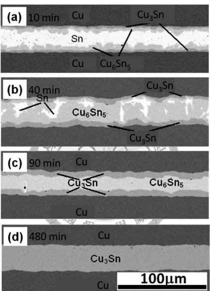
1.3.1 Issue I: Peculiar Microstructural Features Attributed to Space Confinement Li et al. have studied the microstructure feature of 3D IC scaled joints [6], as illustrated in Figure 1.6, Cu/Sn(25m)/Cu sandwiches were reacted at 340 oC for 10-480 min. Figure 1.6 (a) shows that Cu6Sn5 and Cu3Sn forming at each interface and
9
the rest volume in the joint was filled with Sn at 10 min. When the reaction time reached 40 min, as showed in Figure 1.6 (b), grains of Cu6Sn5 growing from the opposite interfaces started to impinge on each other. The original Sn was no longer in the form of a continuous layer, but was separated by the vertically impinged Cu6Sn5
grains. Figure 1.6 (c) displays the microstructure after 90 min, Sn was consumed and the joint was entirely occupied by IMCs of Cu6Sn5 and Cu3Sn. In Figure 1.6 (d), Cu6Sn5
fully disappeared after 480 min, leaving only Cu3Sn in the joint. According to these results, solder in the 3D IC joint is demonstrated having a chance to be fully consumed and transformed into IMCs. One thing deserving more attention is the timing that each step in microstructure evolution happens. Since the reaction temperature in Li’s study is 340 oC which is too high to predict results in the practical packaging process, reasonable temperatures were used in this study to reveal microstructure features in the space confined soldering reaction.
10
Figure 1.6 Microstructure evolution of Cu/Sn(25m)/Cu sandwiches reacted at 340
oC for (a) 10, (b) 40, (c) 90 and (d) 480 min. (Photos taken from [6])
11
1.3.2 Issue II: Impingement and Merging of IMC Grains
In a micro-joint of 3D IC packages, IMC impingement is the inevitable result as the reaction proceeds. However, it is very interesting and surprising that the IMC grains originally growing from the different interfaces can eventually merge into a single one.
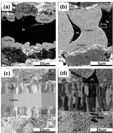
Figure 1.7 shows an example from Li’s study [6]. The focused-ion-beam images were used to visualise the grain contrasts in the Cu/Sn(25m)/Cu joint. Before IMC grain impingement, as showed in Figure 1.7 (a), the microstructure at each interface was very similar to that in the conventional solder joint. The scallop-type Cu6Sn5 formed on the Cu substrate and a very thin layer of Cu3Sn also presented at the Cu6Sn5/Cu interface.
As the Cu6Sn5 grains growing from the opposite interfaces vertically impinged on each other, as showed in Figure 1.7 (b), the two grains were surprisingly merged into a single grain, since no grain boundary was observed within the merged grain. It was very interesting and surprising that two grains originally having different orientations could become merged in such a short time-frame of 10 min. One other interesting finding was that a necking morphology was observed near the centre of the merged grain, as indicated by an open arrow in Figure 1.7 (b). The location of the necking was probably the point that these grains had impinged. This merging process is considered highly relating to the grain coarsening via atomic diffusion, since it is very difficult for a rigid IMC grain changing its orientation via the mechanically rotation. When Sn was fully
12
consumed, Cu3Sn would further grow at the expense of Cu6Sn5, as showed in Figure 1.7 (c) and (d). After the Cu6Sn5 layer became disappeared, the joint was fully occupied by Cu3Sn. As can be seen in Figure 1.7 (d), a boundary located in the middle of the Cu3Sn layers suggesting that the Cu3Sn grains approaching to each other from the opposite direction did not become merged into a single grain.
Recall the fact that Cu6Sn5 grains after impingement can become merged, but the merging behaviour seems not occurring for Cu3Sn phase. A boundary throughout the joint must have great impacts on the joint strength. The merging behaviour has never been observed in the conventional solder joint. Therefore, there is a lack of knowledge about this behaviour itself and the resulting influences. In this study, the microstructure characterisation will be carried out by means of electron backscatter diffraction (EBSD) to uncover the IMC grain merging issues with a main focus on the common soldering reactions.
Electron backscatter diffraction (EBSD), also known as backscatter Kikuchi diffraction (BKD), is a microstructural-crystallographic technique used to examine the crystallographic orientation of many materials, which can be applied to crystal orientation mapping, phase identification, grain boundary and morphology studies. A good example is showed in Figure 1.8 [19], where EBSD analysis successfully reveals the crystallographic information of IMC grains on orientation distribution and grain
13
boundaries between the neighbouring grains. Similar methods will be used in the present study to understand the merging issues.
14
Figure 1.7 Focused-ion-beam images showing the microstructure evolution of Cu/Sn (25m)/Cu sandwiches reacted at: (a) 260 oC for 5 min, (b) 300 oC for 10 min, (c)
300 oC for 480 min and (d) 340 oC for 480 min. (Photos taken from [6])
Figure 1.8 An example of the crystal orientation map and the colour coding of IMC grains. (Photo taken from [19])
15
1.3.3 Issue III: Effects of Solder Volume Reduction on the IMC Growth Kinetics
The solder volume in a 3D IC joint is merely 1/1000 of that in a clip-chip joint. One key issue arising from solder volume reduction is whether or not the growth rate of IMCs remains unchanged when the solder volume goes down. The results are of practical importance to engineers on determining assembly parameters. The correlation between solder volume and the IMC growth rate is the degree of saturation in the solder.
According to previous studies [20, 21], IMC growth is a competitive process between IMC formation and dissolution. Relation of these two factors is showed as Equation 1.1.
k c c Equation 1.1
where c is the concentration of the dissolved material in the bulk of the melt or solution, t is the time, cs is the saturation concentration or solubility, k is the dissolution rate constant, s is the solid specimen surface area and v is the melt volume. The derivative dc/dt represents the change rate of solute concentration in the bulk of the melt or solution during the reaction.
In a soldering reaction with a fixed value of k, s and v, (cs – c) is the driving force that the IMC or substrate material to be dissolved. When (cs – c) = 0, the bulk of melt or solution is saturated and consequently causes a negligible net dissolution. However, if (cs – c) > 0, the net dissolution would occur in the reaction. If the IMC dissolution is
16
retarded, the IMC growth can be promoted as a result. Taking Cu-Sn reaction as an example, Cu reacts with Sn to form Cu-Sn IMCs as the reaction proceeds. As the IMC layer is thickening, IMC dissolution and formation simultaneously occurs. For a 3D IC joint, the solder volume is very small, and the concentration of the dissolved Cu may shortly reach its solubility limit in Sn. When Sn is saturated with Cu, IMC dissolution becomes depressed so that the IMC formation becomes promoted. In the present study, experimental evidence will be used to clarify this issue in Cu-Sn and Ni-Sn reactions.
1.3.4 Issue IV: Rise of Inert Alloy Constituent Concentration Due to Solder Consumption
Alloying modification is a very common way to improve the properties of solders.
In practical, adding Ag or Bi into Sn can lower the melting point of the solder and improve the wettability [22]. Sn-based solders containing Fe, Co, Ni or Zn additives can reduce the growth rate of Cu3Sn and the suppress formation of micro-voids which if present will degrade the joint reliability [23, 24]. Using solders with Cu content can resolve the Au embrittlement problems [25, 26]. Additives of Mn or Ti can improve the solder strength [27]. Among these additives, Ag and Bi are inert to the soldering reaction. Precisely speaking, Ag or Bi atoms are insoluble in Cu-Sn or Ni-Sn IMCs [28-31], and will be rejected and pushed away from the IMC/solder interface as the reaction proceeds. As more and more solder is consumed, the effective concentrations of
17
the inert constituent can increase as schematically showed in Figure 1.9.
Figure 1.9 Schematic drawing showing (a) the inert constituent randomly dispersing in the solder region and (b) the inert constituent is rejected and pushed toward the
centre of the interface.
There is one difference between Ag and Bi: Ag reacts with Sn to form an IMC but Bi does not. The role of Bi is somewhat similar to the impurities in the solder joint. These impurities include organic or inorganic complex agents, acids, sulphates or sulphides, surface levellers, foreign metal atoms, etc. induced in electroplating which is one of the methods that solder is deposited in micro bumps of 3D IC. Most of these impurity molecules or atoms are insoluble in IMCs, and will also be rejected from the reaction.
Following the same logic, the impurity concentration can increase as more and more solder is incorporated into IMCs. When the solder is entirely consumed, the impurity molecules or atoms might even aggregate and decorate along the boundary of IMC grains growing from the opposite directions. In this thesis, a systematically study are made to illustrate the effect arising from inert Ag or Bi in a space confined soldering
18
reaction. Implications of the results will be also discussed.
1.3.5 Issue V: Area-to-volume Ratio Effect Relating to the Surface Finish
Copper base metal on the soldering pads of micro joints has to be coated with a surface finish to preserve the wetting property during the storage period before assembly.
Popular surface finishes under consideration include Au/Ni and Au/Pd/Ni. During soldering, the Au and Pd layers dissolve into solder rapidly [26, 32-38], exposing the Ni layer below. The Au layer is typically deposited by an immersion process and has a thickness of 20 ~ 50 nm, and the Pd layer by an electroless process and is about 50 nm thick. For BGA and flip-chip solder joints, this thickness level of Au and/or Pd surface finish will not become a risk of Au embrittlement. Unfortunately, the problem of Au embrittlement will probably be re-emerged from the solder volume reduction in the 3D IC packaging.
In the BGA technology, the Au layer is often deposited by an electroplating process, and has a thickness as high as 1 m. The presence of Au creates the so-called Au embrittlement problem [26, 35], particularly when the eutectic PbSn solder is used. This Au embrittlement problem can be resolved in the short term by reducing the Au thickness, so that the effective Au concentration in solder is lowered. Nevertheless, as the size of solder joints becomes smaller, the Au embrittlement problem will re-emerge as will be
19
illustrated below. Let us consider a spherical Sn-based solder joint with a radius r sitting on a spherical soldering pad with a radius rpad, as schematically showed in Figure 1.10.
Figure 1.10 The schematic drawing indicating parameters in Equation 1.2 ~ 1.4.
It is assumed that the soldering pad is coated with an Au layer with a thickness of d, and Au is completely dissolved into solder, one can calculate the effective Au concentration in solder based on Equation 1.2.
cAu (wt.%) = 100 A
S A Equation 1.2
where Sn andAu are the density of the solder and Au, respectively. When the mass of solder is much greater than that of Au, Equation 1.2 can be simplified as Equation 1.3.
cAu (wt.%) = 75 A
S Equation 1.3
20
Assuming rpad equals r, one obtains the following equation by using Au=19.3 and
Sn=7.3 (that of pure Sn), Equation 1.3 thus becomes Equation 1.4.
cAu (wt.%) = 198 Equation 1.4
Equation 1.4 shows that, with the same d, Au concentration increases as the dimension of a joint, r, becomes smaller. In the size scale of BGA (r ~ 200 m), cAu can
easily be kept below the safety threshold for Au embrittlement (~ 0.8 wt.%) [39] by keeping the Au thickness thinner than 0.8 m. In the size scale of flip-chip solder joints (r
~ 50 m), Au embrittlement still can be avoided by keeping d below 0.2 m. However,
Au thickness has to be kept smaller than 20 nm in order to have cAu < 0.8 wt.% for 3D IC micro-joints (r ~ 5 m). Nevertheless, for practical purposes, d cannot become thinner than a certain value (~ 20 nm) without losing its effectiveness when the immersion process is used. From this point of view, the Au embrittlement problem may become relevant again in the 3D IC size scaled packaging. The extent and effects of this issue will be studied and discussed.
1.3.6 Issue VI: Soldering Reaction Induced Volume Shrinkage
In the reaction between solders and substrates, there is often having net volume shrinkage when IMCs form. Assuming n mole of solder metal A reacts with m mole of
21
substrate metal B to form a AnBm IMC, as denoted as Equation 1.5.
nA mB A B Equation 1.5
The theoretical shrinkage value can be calculated based on Equation 1.6 with given molar volumes of IMCs and pure metals.
∆V V
VA B – VA VB
VA VB Equation 1.6
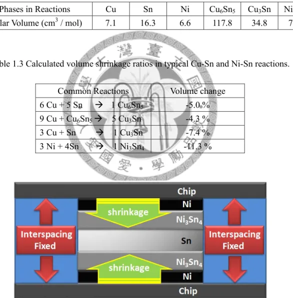
where V is volume and ΔV / V is the theoretical volume change ratio. The molar volumes for common phases in the soldering reactions are collected in Table 1.2 [40, 41]. In addition, Table 1.3 illustrates the calculated volume shrinkage ratios for the typical Cu-Sn and Ni-Sn reactions.
Taking the Ni-Sn reaction as an example, when 3 moles of Ni react with 4 moles of Sn to form 1 mole of Ni3Sn4, the ratio of volume shrinkage is equal to [75.3-(3x6.6-4x16.3)] / 3x6.6+4x16.3 = -0.113, or -11.3%. Under the condition that the solder joint height is much smaller than the width or depth of the joint, a majority portion of the volume shrinkage dissipates through the vertical direction. In the extreme case that the width and depth of a joint are considered infinite compared to the height of a joint, the volume shrinkage can only be dissipated through the vertical direction. In such a situation, the joint height has to shrink by 11.3% in the case of Ni3Sn4. Such an appreciable
22
shrinkage raises the potential of introducing sizable internal stress, especially in the case that the interspacing between the upper and lower chips is rigidly fixed, as showed in Figure 1.11.
Table 1.2 Theoretical molar volume values of common phases in soldering reactions.
(data obtained from [40, 41]).
Table 1.3 Calculated volume shrinkage ratios in typical Cu-Sn and Ni-Sn reactions.
Common Reactions Volume change 6 Cu + 5 Sn 1 Cu6Sn5 -5.0 % 9 Cu + Cu6Sn5 5 Cu3Sn -4.3 % 3 Cu + Sn 1 Cu3Sn -7.4 %
3 Ni + 4Sn 1 Ni3Sn4 -11.3 %
Figure 1.11 The schematic drawing showing the volume shrinkage issue.
Phases in Reactions Cu Sn Ni Cu6Sn5 Cu3Sn Ni3Sn4
Molar Volume (cm3 / mol) 7.1 16.3 6.6 117.8 34.8 75.3
23
To fully appreciate the significance of this volume change, one simply has to note that the volume change for the phase transformation between liquid water and ice is only about 9%, and the stress induced by water-ice transformation is the key reason of degradation for many large scale concrete or stone structures. It can be anticipated that the 11.3 % volume shrinkage ratio, for Ni-Sn reactions, definitely have chances to impact joint properties. In this study, experimental evidence will be used to illustrate the effect of volume shrinkage for Ni-Sn system during the interfacial reaction, and the implication will be also proposed.
24
1.4 Aims of the Thesis
This thesis is aimed at establishing fundamental knowledge concerning critical new issues in soldering reactions arising from the space confinement. There are six issues to be addressed in this thesis, including I. Peculiar Morphology of Cu/Sn/Cu
and Ni/Sn/Ni Reactions, II. Impingement and Merging Behaviour of IMC Grains, III.
Effects of Solder Volume Reduction on IMCs Growth Kinetics, IV. Effects of Inert
Alloy Constituents in the Space Confined Soldering Reaction, V. Area-to-volume
Ratio Effects Relating to the Surface Finish and VI. Soldering Reaction Induced
Volume Shrinkage. Theoretical analysis and experimental data will be used to demonstrate the extent and effects of these critical issues. Implications of results will also be proposed and discussed.
25
2.0 EXPERIMENTAL DETAILS
2.1 Sample Preparation and Experimental Procedure
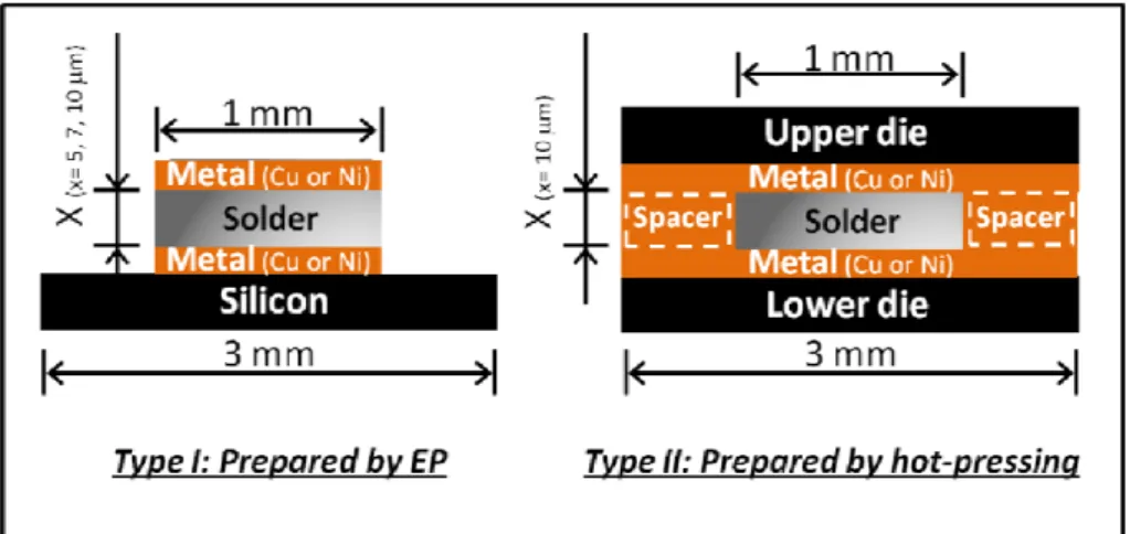
Figure 2.1 schematically displays the sandwiched samples used in the present studies that were prepared through two different approaches. In approach I, sandwiches were prepared by merely electroplating each metal layers, i.e Cu, Ni and solders, sequentially on the Si wafers with the pre-sputtered Cr (300 Ǻ)/Cu (3000 Ǻ) seed layer, as showed in Figure 2.2. Noticeably, there was no bonding process needed so that the melting or solidification effects were negligible when the experiment carried out with this type of samples. For some cases that could not be accomplished by approach I, a bonding process was applied to prepare the sandwiches, as schematically showed Figure 2.3. Before bonding, a fluxed solder sphere was placed onto the lower die, and the upper die was then upside down placed on the solder sphere. Lower die, together with the upper die and the in-between solder sphere were kept on a hot plate at a fixed temperature. A force was loaded on the upper die pushing it toward to the lower die when the solder is molten. The force was expected to ensure a close contact between the upper and the lower die, but it has no effect on the joint quality since the force was only loaded on the spacer, which was designed to determine the solder thickness, rather than on the soldering interface. The heating time is 1 min measured after the solder is molten,
26
and the sample was then cooled down to room temperature on an aluminium plate in air.
For various purposes of experiments, samples were subjected to further heat treatments such as solid-liquid reaction or the solid-state aging.
For all sandwiches, the aspect ratios of the solder layer were really low since the solder thickness was simply 5-10 m but the lateral dimension of the joint was 1000 m.
Under such configurations, the space was confined along the vertical direction, and along the lateral directions the space could be considered as infinite. With the edge regions ignored, the direction of the inter-diffusion fluxes can be considered limited to the vertical direction, i.e., the space-confined direction.
Among all solder materials used in experiments, pure Sn (99.99) and Sn3.5Ag (wt.%) are commercial products from CERAC-TM incorporated and Senju Metal Industry Co., respectively. Other Sn-based alloys are prepared by mixing molten elements in vacuum. Proper amount of pure elements were weighted and put into quartz tubes. The tubes were vacuum-sealed and then storage at 800 oC for 240 h ensuring that elements were well mixed. Finally, the tubes were water quenched and cut into small pieces. The alloy compositions were verified using inductively coupled plasma atomic emission spectroscopy (ICP-AES) to confirm the composition uncertainty is acceptable.
27
Figure 2.1 Schematic drawings showing two types of sandwiches prepared by electroplating and hot-pressing bonding.
Figure 2.2 Schematic drawings showing the type I sample preparation via electroplating.
Figure 2.3 Schematic drawings showing the type II sample preparation via hot-pressing bonding.
28
After the solid-liquid reactions or solid-state aging, sandwiches were mounted in epoxy and subjected to a metallographic grinding-polishing process to reveal the cross-sectioned microstructures. To avoid the occurrence of artefacts due to mechanical polishing, some specimens were cross-sectioned by using an ion beam polisher (HITACHI E3500) which was known to have the capability of producing a relatively high quality and artefact-free surface. The polished specimens were examined by scanning electron microscopy (HITACHI S-3000N) with an energy dispersive X-ray analysis detector (BRUKER AXS XFlash detector 5010). In some particular cases that required high accuracy of composition examinations, electron probe micro-analyzer (JEOL JXA-8200) was conducted to provide high quality composition determinations.
In addition, EBSD studies were performed on the cross-section of sandwiches using a field emission electron microscope (JEOL 7001F) with EBSD system (EDAX/TSL Technology) operated at 20 kV. The crystallography references for Cu6Sn5, Cu3Sn and Ni3Sn4 are [42-44].
29
2.2 Theories and Assumptions for Kinetics Analysis
The thickness of the reaction products was measured using image analysis software.
The thickness was defined as the phase area divided by its linear length. For studying the IMC growth kinetics, a couple of assumptions were made. First, the interfacial reactions that occur at the two solder-to-substrate interfaces are assumed to be identical for simplification so that only one sides of the interface is considered. Accordingly, the thicknesses of the IMCs formed at the two interfaces are averaged to improve accuracy.
Second, the effect of simultaneous IMC dissolution is eliminated due to the very limited solubility of the substrate material in solder at the desired reaction temperatures. Finally, to quantify the growth of IMCs, the relationship between the IMC layer thickness and the aging time is described by fitting the experimental data to an empirical power law, l = k t n Equation 2.1 where l is the IMCs layer thickness, t is the reaction time, n is the time exponent and k is the constant. In most soldering reactions, the IMC growth is regarded as a diffusion-controlled process. Thus, the n value is assumed as 0.5, and k represents the parabolic growth constant. Additionally, activation energies for the IMC formation and growth will be calculated by using the Arrhenius equation illustrated below,
ln k = ln k0 Q
RT Equation 2.2
30
where k is the parabolic constant, k0 is the pre-exponent factor, Q is the activation energy, R is universal gas constant (8.314 J/mol K) and T is the reaction temperature (K).
In order to clarify the effects of solder volume on the IMCs growth behaviour, a number of literature data will be collected for comparison. The literature data are assumed obeying these assumptions.
31
2.3 Alpha-step measurement
Considering the type I sample showed in Figure 2.1, the vertical height of the sandwich is free to change along the vertical direction when the volume is decreased. In other words, the volume shrinkage can be characterised by measuring the height change of the sandwich. In the present study, an alpha-step profiler (Veeco DEKTAK 6M STYLUS PROFLIER) was conducted to measure the surface profile of the sandwich after sample was subjected to a desired aging time, for which the thickness change of the sandwich can be monitored. The experimental setup of the alpha-step measurement is schematically showed in Figure 2.4. The sample used in this study was Ni/Sn(5m)/Ni sandwiches. The main reason of choosing Ni/Sn/Ni system is that Ni-Sn reaction can induce the largest volume shrinkage, i.e., 11.3% as the reaction proceeds.
Before aging, the surface profile of the as-plated sandwich was probed as the base line, and for comparison with that of samples was subjected to further aging treatments. The lateral scanning rate was 5 mm/min, under this condition, the resolution of the measurement along the vertical direction was about 10 Å, which was much smaller than 750 nm which is a theoretical value of thickness reduction corresponding to 11.3 % volume shrinkage for the Ni-Sn reaction. Therefore, the resolving power of alpha-step measurement was considered well sufficient.
32
Figure 2.4 The experimental setup of the alpha-step measurement.
33
3.0 RESULTS AND DISCUSSION
3.1 Peculiar Morphology of Cu/Sn/Cu and Ni/Sn/Ni Reactions
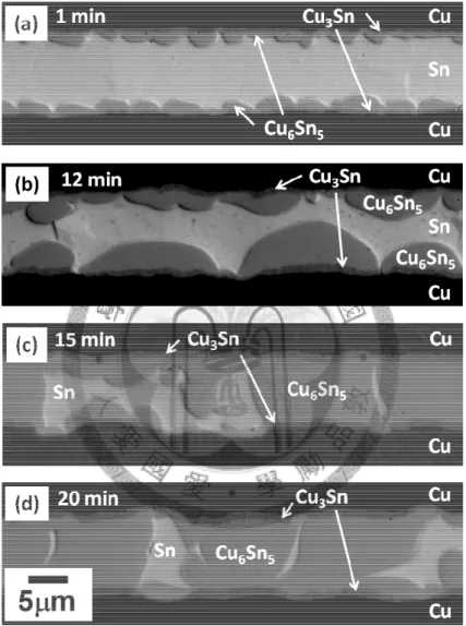
To simulate the assembly process, Cu/Sn(10m)/Cu sandwiches were reacted at 250
oC for 1, 12, 15, and 20 min. The cross-sectional scanning electron micrographs are
showed in Figure 3.1 (a)-(d). In the as joined condition, a layer of typical scallop-type Cu6Sn5 was observed at each interface. In addition, a thin layer of Cu3Sn was also visible between Cu and Cu6Sn5. The rest space in the joint was filled with Sn. After 12 min of the reaction, as showed in Figure 3.1 (a), the size of Cu6Sn5 grain became greater, and the numbers of grains were reduced. It was found that the Cu6Sn5 grains growing from the opposite directions approached to each other as showed in Figure 3.1 (b).
When the reaction time reached 15 min, as showed in Figure 3.1 (c), Cu6Sn5 grains from the opposite sides did impinge to each other at certain places, becoming large grains that spanned across the entire joint. There was a necking morphology observed at the grains spanning across the interfaces, as indicated by open arrows. The location of the necks was probably the point where the original grains had impinged. Very interestingly, there was no visible grain boundary within the large grains spanning across interfaces. A possible reason was that the vertically contacted grains had already merged into a single crystalline grain, so that there was no grain boundary within the grain. In Figure 3.1 (d),
34
most of the Cu6Sn5 grains had become large grains that spanned across the two interfaces after 20 min. At this time Cu6Sn5 occupied a quite large portion of volume in the joint. It was worth mentioning, once a certain number of IMC grains were vertically impinged, these IMC grains acted as columns or pillars in the joint, which somewhat provide the mechanical strength of the joint. Let’s consider a 3D IC package as showed in Figure 1.3, the joint once contains a certain number of grains spanning across the interfaces, which is able to accept a next chip stacking on the original level without crashing the joint. Hence, the time-to-impinge is a critical parameter to the manufacturer. The time-to-impinge is actually a function of assembly parameters such as solder thickness and bonding temperature. For instance, the time-to-impinge in the reaction showed in Figure 3.1 is 15 min. While 15 min of the reaction time does seem excessive at first glance, it should be noted that the time-to-impinge can reduce as the solder thickness reduced or the reaction temperature increased.
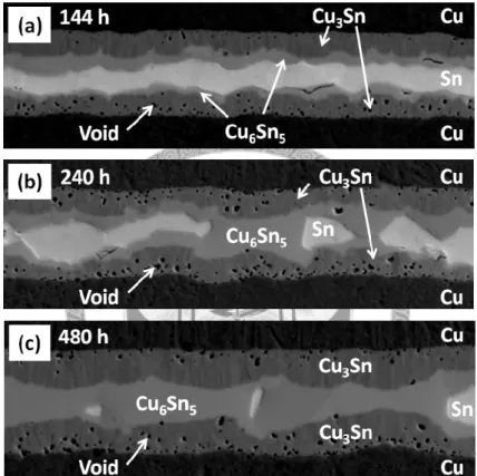
Up to now, there is yet a well-established agreement on whether or not the solder material should be fully transformed into IMCs just in the assembly process. In some cases, the IMC grain impingement may not occur in the solid-liquid soldering reaction, but it would eventually occur during the operation of the devices. To simulate the solid-state reaction of joints, Cu/Sn(10m)/Cu sandwiches were kept at 150 oC for studying the microstructure evolution. Scanning electron micrographs showed in Figure
35
3.2 illustrates the interfacial morphology of 144 ~ 480 h aged samples. At 144 h, the IMC species were Cu6Sn5 and Cu3Sn at each interface as showed in Figure 3.2 (a).
Instead of forming as scallop-type, the Cu6Sn5 was in the form of layer-like during the solid-state aging process. There were a certain number of micro-voids observed within the Cu3Sn layer. The Sn phase was still in the form of a continuous layer. When the aging time reached 240 h, Cu6Sn5 and Cu3Sn layers had become thickened. The Cu6Sn5
grains growing from the opposite directions were vertically contacted to each other, isolating the Sn layer into several pockets, as showed in Figure 3.2 (b). At this moment, the thickness of Cu3Sn was slightly greater than that of Cu6Sn5, this Cu3Sn–to-Cu6Sn5
thickness ratio is similar to the results reported in [45, 46]. The interfacial morphology of 480 h aged sample was presented in Figure 3.2 (c), the joint was almost occupied by IMCs, i.e., Cu6Sn5 and Cu3Sn, leaving only a few Sn pockets in the joint. The reaction takes simply 480 h to transform nearly the entirety of Sn layer into IMCs. For some other cases which have joints containing a thinner Sn layer, the transformation time can be even shorter. These results demonstrate that Cu/Sn/Cu joint in such a small size scale in 3D IC packages, the solder, i.e., Sn phase, inevitably will be fully consumed in a reasonable duration, leaving only IMC in the joint. With the further prolonged reaction time, the Cu3Sn can grow at the expanse of Cu6Sn5, and the microstructure of joint ends up with a completely occupation of Cu3Sn, as showed in Figure 1.6 (d) and Figure 1.7
36
(d) [6, 47, 48]. A key concern of such all-Cu3Sn joint is the massive formation of micro-voids that will probably degrade the joint strength and the reliability.
Figure 3.1 Micrographs showing the Cu/Sn(10m)/Cu reaction at 250 oC for (a) 1, (b) 12, (c) 15 and (d) 20 min.
37
Figure 3.2 Micrographs showing the Cu/Sn(10m)/Cu bonded at 250 oC and then aged at 150 oC for (a) 144, (b) 240 and (c) 480 h.
38
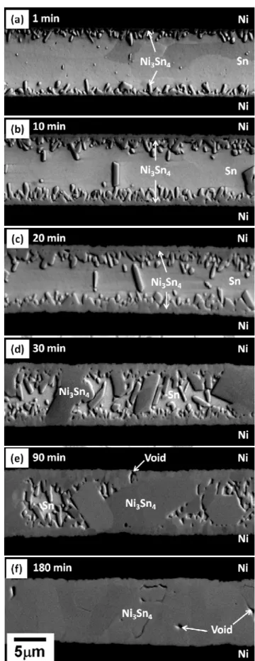
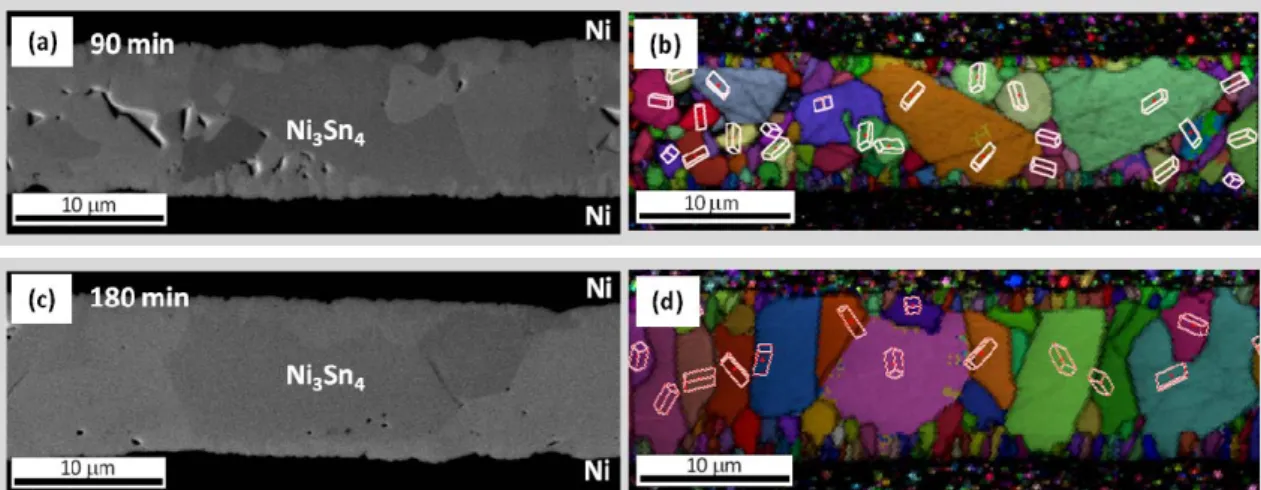
Figure 3.3 illustrates the microstructure evolution of Ni/Sn(10m)/Ni reacted at 250 oC for 1 ~ 180 min. In the as-joined condition at 1 min, an irregular layer consisted of the so-called whisker-like Ni3Sn4 formed at each interface, as showed in Figure 3.3 (a). In the following 20 min, Ni3Sn4 layer gradually became thickened as presented in Figure 3.3 (b) and (c). Meanwhile, there were a few Ni3Sn4 particles locating within the Sn region. These particles were either formed during the solidification or broken off from the interfaces. At 30 min of the reaction, as showed in Figure 3.3 (d), Ni3Sn4
grains from the opposite interfaces started to impinge on each other. At this time, the Sn layer was separated into many small pockets. As showed in Figure 3.3 (e), the joint was nearly occupied by Ni3Sn4 after 90 min, and there were a few voids located in the joint.
When the reaction reached 180 min, as showed in Figure 3.3 (f), Sn was completely incorporated into Ni3Sn4. Interestingly, some voids and cracks were observed within the Ni3Sn4 layer, especially along the grain boundaries. The reasons of the void formation are the reaction induced volume shrinkage and the IMC impingement, which will be later illustrated in chapter 3.4.1. Considering the microstructure after 20 min, Ni3Sn4
occupied about half of the joint. This suggests that if the Sn thickness had been 5 m, instead of 10 m here, the entire joint would have been completely occupied by Ni3Sn4. Surprisingly, the all-IMC joint is achieved in 3D IC packages even with use of Ni substrate which was considered having a much slower reaction rate with solders.
39
Figure 3.3 Micrographs showing the Ni/Sn(10m)/Ni reaction at 250 oC for (a) 1, (b) 10, (c) 20, (d) 30, (e) 90 and (f) 180 min.
40
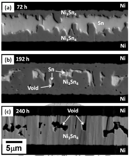
Scanning electron micrographs showed in Figure 3.4 presents the interfacial morphology of Ni/Sn(10m)/Ni solid-state aged at 150 oC for 72-240 h. The sandwiches were prepared through merely electroplating, namely the solder did not experience melting during sample preparation. At 72 h of aging, an irregular layer composed of whisker-like Ni3Sn4 formed at each interface. However, the diameter of the whickers was much greater than that in the solid-liquid reaction. When the reaction time reached 192 h, Ni3Sn4 grains from the opposite interfaces had impinged on each other, and the Sn layer became separated into many small pockets. It should be noticed that some voids were observed. An ion-beam polishing process, which is known to have the capability of producing relatively high quality and artefact-free surface, was used to prepare the cross-section of a 240 h aged Ni/Sn(10m)/Ni sandwich, for double checking the void formation. The fact that voids existing in surface prepared by ion beam polisher suggests that these voids are an intrinsic feature of such reaction under space confinement. In fact, these voids consistently showed up in all of our Ni/Sn/Ni samples aged at all temperatures as long as all Sn had been consumed. The existence of these voids raises serious reliability concerns as these voids will no doubt weaken solder joints.
41
Figure 3.4 Micrographs showing the Ni/Sn(10m)/Ni aged at 180 oC for (a) 72, (b) 192 and (c) 240 h. The surface showed in (c) was prepared by using an ion beam
polisher.
In summary, no matter what the substrate material, i.e., Cu or Ni, is used in 3D IC micro-joints the Sn solder inevitably will be fully consumed and incorporated into IMCs during the assembly process or the operation duration of devices. For Cu/Sn(10m)/Cu reactions, the IMC grain impingement occurs within 15 min of the reaction at 250 oC.
Once IMC grains vertically contacted, the joint is considered available to accept a next stacking without crashing the joints in the original level. The required
42
time-to-impingement is 30 min for Ni/Sn(10m)/N. Even through the require time is longer than that of Cu/Sn(10m)/Cu reactions, the impingement can also occur in a reasonable time as the Ni/Sn/Ni joints contain with a thinner solder layer, or reacted at a higher temperature. Voiding in the joint is always a key concern resulting in the degradation of reliability. Unfortunately, the void formation occurs in both Cu/Sn/Cu and Ni/Sn/Ni reactions. For Cu/Sn/Cu reactions, the voiding problem can be resolved by alloying a minor addition of Fe, Co, Ni or Zn in solders [23, 24]. For Ni/Sn/Ni reactions, voiding is a unique behaviour in the space confined reaction, which do not happen to the conventional flip-chip or BGA solder joints. In this study, it is demonstrated that using Sn-Ag solder is able to eliminate the voids. The detailed description will be present in chapter 3.4.1.
43
3.2 Impingement and Merging Behaviour of IMC Grains
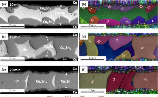
Figure 3.5 illustrates scanning electron micrographs and the corresponding EBSD grain orientation maps of Cu/Sn/Cu joints reacted at 250 oC for 10 ~ 20 min.
Micrographs in Figure 3.5 (a), (c) and (e) display the typical microstructure evolution of the Cu/Sn/Cu reaction under space confinement. The EBSD orientation maps showed in Figure 3.5 (b), (d) and (f) are corresponding to Figure 3.5 (a), (c) and (e), respectively.
On the EBSD maps, the crystal lattice symbols located on IMC grains indicate the distribution of the Cu6Sn5 grain orientation in the three dimensional space. When the reaction time was 10 min, there was no Cu6Sn5 grains had vertically contacted as showed in Figure 3.5 (a) and (b). It should be noticed that there was no particular preferred orientation relation among the Cu6Sn5 grains at the interfaces. As the reaction reached 15 min, as showed in Figure 3.5 (b) and (c), a few Cu6Sn5 grains had vertically impinged on each other, and merged into a large grain that spanned across the interfaces.
Very interestingly, only one grain orientation was identified on each large grain spanning across the interfaces. This implied that the grains originally having different orientations became merged into a single crystalline grain after impingement. The same phenomenon was again observed as the reaction time reached 20 min, as showed in Figure 3.5 (e) and (f). At 20 min, the entire joint, visible in the figure, was occupied by merely three large Cu6Sn5 grains which have a averaged diameter of about 15 m.