國立臺灣大學電機資訊學院光電工程學研究所 碩士論文
Graduate Institute of Photonics and Optoelectronics College of Electrical Engineering and Computer Science
National Taiwan University Master Thesis
奈米音波於砷化鎵奈米柱之波導模態
Nano-Acoustic Guided Waves in GaAs Nanorods
吳岳駿 Yueh-Chun Wu
指導教授:孫啟光 博士 Advisor: Chi-Kuang Sun, Ph.D.
中華民國 101 年 1 月
January, 2012
誌謝
在台大光電所待的兩年再多一點的日子裡,能夠完成一本碩士論文,首先得 感謝我的指導教授,孫啟光老師。在奈米柱波導這個研究裡,總是被很多問題迷 惑而使得自己停滯不前,在我已經不知道該怎麼辦的時候,若不是老師對我的耐 心與包容,現在的我可能也還深陷在某個特定問題而無法自我放棄。老師的意見 與建議總是能讓偏離軌道的我再走回來,在時間最急迫的時候,也還是願意花時 間跟我討論,這個研究,如果不是老師的真知灼見,我可能還是迷惑在眾多實驗 數據內而不知該如何解釋。每次的跟老師討論,總覺得自己的不足與愚昧,往往 卡住在某個細節,卻失去了整個研究的宏觀的觀點。在這兩年多的訓練裡,老師 總是不斷的提醒我,身為一個研究生應該有的態度與看法。雖說完成了一本碩士 論文,但實在是不覺得自己真的學會了如何做好學術研究,但至少在老師的帶領 下,自己或多或少也有了一些長進。真的非常感謝孫啟光老師。
這本論文的完成也要感謝口委老師們的寶貴意見與指正,感謝中研院應科中 心的施閔雄教授、凝態中心的張玉民教授、以及應力所的吳政忠教授,讓這本論 文能更趨於完整。另外非常感謝施閔雄老師以及施老師實驗室幫忙長樣品的學長 姐們,如果不是學長姐的幫忙,這個研究不會有現在的結果。
接著感謝在超快光學實驗室的大家:昱傑學長,是我們奈米組的大學長,當初 自己剛進入實驗室時,學長教會了我很多東西,從學長身上,我也學到了做研究 的思考邏輯與推敲的一點皮毛。不得不說,學長真的很厲害。感謝建誠學長,第 一次在奈米柱實驗上的成功,是跟學長一起的熬夜接力實驗,還有尤其感謝學長 在最後的交接以及在文章上的幫忙。感謝阿賓哥,在製程與樣品的資訊上,給了
相當多的寶貴意見,如果不是學長幫忙照關鍵樣品的 SEM,可能現在自己還不知 道該怎麼辦,真得非常感謝。感謝後來加入實驗室的 P.A.,如果不是學長的幫忙,
自己在 OPO 的實驗不會這麼順利,也感謝 P.A.每次都很有耐心聽我用破英文在討 論事情,在奈米柱的討論上,P.A.給了相當多的意見,這點讓我非常感謝。阿胖學 長,還好每次熬夜做實驗時,你都還在,還可以一起找喝咖啡吃消夜,讓每次熬 夜孤單做實驗的我還感覺有一個伴。還有思齊,昭勳,任棠,子芳,在同屆裡,
我真的覺得自己是最弱的一個,大家真的都很厲害,也祝福思齊和子芳的博士班 能夠順利,昭勳畢業後可以做自己想做的事,任棠能夠順利出國。孝倫,真是不 好意思,自己身為學長卻沒有好好帶你,反倒是你在研究上一直幫助我,真的非 常感謝。也非常感謝怡如在課業上還是實驗時間上的大方幫助。還有 Rebecca,感 謝妳總是跟我們站在一起在面對教授,蕾姐的關心與打氣,在最後的低潮時期,
給了我相當大的鼓勵,最後還有實驗室的其他大家,真的非常感謝,在研究所的 兩年多,其實自己真的很少參與大家的活動,感謝大家還這麼的包容我,還願意 給我這麼多的幫助。能夠認識各位,實在是自己的福氣。
另外還有感謝俊儒,熊,郭老大,雖然不是同實驗室的,但卻也給了我很多 的關懷與幫助。紫微姐,是個好相處的人,總是願意拿出甜心卡讓大家分享,祝 福妳在未來的工作能有好的發展。幾米,雖然覺得你很兇,但是其實內心是個好 人。湯湯,在後來雖然很少聯絡,但至少很高興曾經有你相伴的日子。翁左庭和 柳中原,非常感謝你們一直對我的包容,在你們面前,我總是厚著臉皮的尋求你 們的幫助,你們也總是不厭其煩的伸出援手,在這兩年的有很多的難過與開心,
身為最好的朋友,你們給了我很大的力量。老呂,感謝你的 Ansys 教學,腦包民,
和老褚,感謝你們帶給我的搞笑和樂觀,最後還有施哥,讓台南也能成為我心情
難過時的避風港之一。
佩吟,感謝在這兩年來一直的幫我加油與打氣,妳教會我很多事情,妳的樂 觀,總是能讓沮喪的我很快恢復,有妳的陪伴,應該是我多輩子修來的福氣。還 有特別感謝高中的班導鄧金城老師,雖然畢業了六年多,但老師還是很關心我們 這群已畢業的小毛頭們,老師一直是我心靈上的支柱之一。最後要感謝的是我的 家人,我的爸爸,奶奶,你們無怨無悔的付出,並且總是支持我的決定。在我最 低潮的時候,才真的發現,家人是我真正的依靠,是支持我的最大力量。念完這 兩年多,才發現要感謝的人著實太多,這本論文,雖然自己仍覺得不夠完美,但 至少自己盡力,這本論文謹獻於所有關心我和幫助過我的人們,還有我最摯愛的 家人們。
中文摘要
利用超快光學方式來產生並偵測具奈米尺度波長與次兆赫(sub-terahertz)頻率 音波的技術(picosecond ultrasonics) 已廣泛地被用來評估與研究奈米尺度下的物理 現象。先前研究中,因忽略邊界效應,激發之音波主要被視為於晶體塊材內傳播 的縱波與橫波模態。而另一方面,奈米結構之共振特性(confined acoustic modes)雖 亦被大量地探討與研究,然而音波因受奈米結構邊界之侷限而產生離散波導模態 (guided modes)與特定色散關係的傳播特性卻鮮少被討論。故在此研究內,我們欲 利用激發探測法(pump-probe technique),以具奈米厚度之金膜吸收激發光(pump beam)而熱膨脹,進而產生奈米等級波長之音波在砷化鎵奈米柱內以波導模態傳 播,再以探測光(probe beam)偵測其反應。在理論計算上,我們用發展於共振超音 波頻譜分析(resonant ultrasound spectroscopy)之計算方法處理砷化鎵奈米柱的非等 向性,在假設柱體為無限長,邊界沒有受應力的條件下,可得被侷限在奈米柱內 傳播之波導模態的色散關係與特徵場型。而在實驗上,我們對一系列不同尺寸的 奈米柱分別在不同的探測光(probe beam)波長下做量測,由實驗結果我們歸納:(1) 在探測光波長為 880 奈米,所觀測到的震盪訊號主要來自於柱體的徑向呼吸震動 模態 (radial breathing mode),然而(2)在波長為 1120 奈米的探測光的條件下,柱體 直徑小於 300 奈米以下的樣品,所觀測到的震盪訊號主要來自於表面奈米金盤的 振動。在此情況下,此訊號同時伴隨著回音的產生。我們推測此震盪訊號的轉變 和奈米金盤的侷域表面電漿子共振(localized surface plasmon resonance)有關。藉由 其效應,奈米金盤可視為一感測器去偵測由底部反射回來的回音。此回音代表由 金盤振動所耦合的波導模態在柱體內的傳播以及在柱底不連續介面的反射行為。
由實驗結果分析,音波在奈米柱內的確呈現出不同於塊材內的傳播行為。且其回 音時間符合波導理論預期。同時實驗中也顯示,不同模態因介面不連續所造成的
反射率不同,其中我們推估主要激發之低頻模態其反射率為 0.5
0.2
。關鍵字:奈米超音波、超快光學、奈米柱、音波波導模態、共振超音波頻譜分析、
色散關係、徑向呼吸模態,侷域表面電漿子共振。
ABSTRACT
Picosecond ultrasonics for its mechanisms of generation, detection and applications has been widely studied. Most of previous studies treated the excited acoustic waves as longitudinal and transverse modes due to the neglect of boundary confinement. On the other hand, using femtosecond lasers to excite the confined acoustic modes of nanostructures were also been discussed greatly, but the acoustic guided modes confined to the nanostructures were rarely discussed. In this thesis, we used ultrafast optical pump-probe technique to generate and detect nano-acoustic waves (NAWs) confined to a GaAs nanorod. In our designed structure, a gold nanodisk that deposited on the top of the nanorod was designed to acts as an opto-acoustic transducer.
NAWs are launched for the thermal-induced vibration of the disk, and then the waves evolve to guided modes that propagate inside the nanorod. In theory, continuum linear elastic model – resonant ultrasound spectroscopy (RUS) is adopted for the anisotropic elastic properties of GaAs. Under the assumptions of infinite rod length and stress free boundary conditions, the dispersion relation of guided modes is obtained. From experiment, we concluded the detection sensitivity of acoustic responses of the designed samples depend on the probe wavelength: (1) for near-infrared probe (880nm), the dominating oscillatory signal observed is induced from the radial breathing mode of GaAs nanorods. However, (2) for infrared probe (1120nm) condition, the dominant signal converts into the vibration of nanodisk. Under this scheme, echoes with relatively slow velocity are observed as well. We suggested the intervention of localized surface plasmon resonance (LSPR) should be the key to the change of the signal. With the aid of LSPR, the Au nanodisk is not only a transducer but also a highly sensitive acoustic
detector to detect the returning echo. The roundtrip time of observed echo shows a good agreement with the simulation of the anisotropic waveguide theory. The results reflect the fact that propagation of NAWs confined to nanostructures are different to that in bulk crystal. Additionally, in this thesis we further demonstrated the reflection coefficient of the fundamental mode at the rod-substrate interface is roughly 0.5
0.2
, while the other modes of higher frequency suffer lower reflection for the issue of mode matching between the nanorod and the substrate.Key Words: Nano-acoustic waves (NAWs), ultrafast optic technique, nanorod, guided modes, radial breathing mode, resonant ultrasound spectroscopy (RUS), dispersion relation, localized surface plasmon resonance (LSPR).
CONTENTS
口試委員會審定書... #
誌謝 ... i
中文摘要 ... iv
ABSTRACT ... vi
CONTENTS ... viii
LIST OF FIGUREs ... xi
LIST OF TABLEs ... xvi
Chapter 1 Introduction ... 1
1.1 Picosecond Ultrasonic (Nano-Acoustic Waves) ... 1
1.2 Femtosecond Pump-Probe Technique ... 2
1.3 Motivation ... 3
1.4 Thesis Structure ... 5
Reference ... 7
Chapter 2 Designed Sample and Experimental Setup ... 10
2.1 Designed Structure of Samples ... 10
2.2 Experiment Setup ... 15
2.2.1 Experiment Setup (probe: 880nm, pump: 440nm) ... 15
2.2.2 Experiment Setup (probe: 1120nm, pump: 390nm) ... 17
Reference ... 19
Chapter 3 Acoustic Dynamics of Laser-Heated Periodic Nanorod Structures .. 20
3.1 Radial Breathing Mode of Nanorods ... 20
3.2 Surface Acoustic Waves in Surface-Patterned Structures ... 22
3.3 Backward Brillouin Oscillation ... 23
3.4 Vibration of Metallic Nano-objects ... 24
Reference ... 27
Chapter 4 Nano-Acoustic Guided Waves in Cylindrical Nanorods ... 29
4.1 Continuum Elastic Theory ... ... 29
4.2 Acoustic Waves in Bulk Crystals ... 31
4.3 Acoustic Waves in Finite Solid – Waveguide Theory ... 32
4.4 Acoustic Guided Waves in an Isotropic Cylindrical Rod ... 32
4.5 Acoustic Guided Waves in an Anisotropic Cylinder Waveguide ... 35
4.5.1 Variation Method ... 36
4.5.2 Basis Function ... 37
4.5.3 Classification of Normal Modes ... 39
4.5.4 Comparison with Pochhammer Chree Theory ... 40
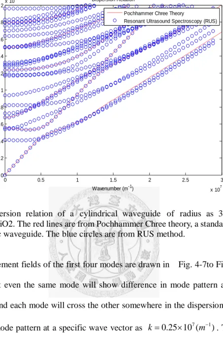
4.5.5 Dispersion Curve and Mode Distribution of Guided Waves in GaAs NRs ... 45
Reference ... 47
Chapter 5 Experimental Results and Discussion ... 49
5.1 Experiment Results (probe 880nm, pump 440nm) ... 49
5.2 Experimental Result (probe 1120nm, pump 390nm) ... 53
5.2.1 Frequency Domain Analysis ... 56
5.2.2 Detection Mechanism for the Infrared Probe (1120nm) ... 61
5.2.3 Time Domain Analysis... 62
5.2.4 Group Velocity of Acoustic Wave Packet ... 64
5.2.5 Roundtrip Loss Inside the GaAs Nanorod ... 69
5.2.6 Backward Brillouin Oscillation ... 75
Reference ... 80
Chapter 6 Summary and Future Work ... 83
LIST OF FIGURES
Fig. 1-1 Schematic diagram of a femtosecond pump-probe experiment ... 3 Fig. 2-1 Schematic diagram of an Au-attached GaAs nanorod array sample. An Au layer of nano-thickness was deposited onto the top of GaAs nanorod to serve as an opto-elastic transducer. ... 11 Fig. 2-2 Flow chart of the process for manufacturing Au-attached GaAs nanorods. 13 Fig. 2-3 SEM image of the Au-attached GaAs nanorods array. (a) Side view of the nanorods, the height of the rods is ~720nm from the image, and (b) top view of the nanorods, the diameter is around 340nm from the image. ... 13 Fig. 2-4 Flow chart of Au-attached GaAs nanorods array... 14 Fig. 2-5 SEM image of the Au-attached GaAs nanorods array. (a) Top view of GaAs nanorod, the diameter is around 256nm, and the period is 355nm from the image. (b) Side view, the height is ~ 720nm. (The sample was made by Hsiang-Yu Chou, and the SEM images were taken by Hung-Ping Chen.) .. 14 Fig. 2-6 The schematic diagram of the two color reflection pump-probe system for probe:860~920nm, and pump:430~460nm. ... 18 Fig. 2-7 The schematic diagram of the two color reflection pump-probe system for probe:1150nm (from OPO), and pump:390nm (from tunable modelock Ti-sapphire laser). ... 18 Fig. 3-1 Displacement field of radial breathing mode of a nanorod. Pure radial expansion and contraction is observed. (Reprinted with permission from [3.4]. Copyright 2010 American Chemical Society.) ... 21 Fig. 3-2 Schematic diagram of SAWs in the periodic surface-patterned structure. .. 23 Fig. 3-3 Schematic representation of backward Brillouin oscillation. The incident
probe was drawn in oblique for clear illustration. ... 24 Fig. 3-4 Schematic diagram of generation of NAWs induced from the thickness vibration of metal thin film. ... 26 Fig. 3-5 Schematic diagram for radial vibration of Au nanodisk induced by the illumination of pump beam. The disk is attached onto a GaAs nanorod. .... 26 Fig. 4-1 A 1D model for propagation of disturbance along a chain of atoms. The Springs represent the interactions between atoms. ... 30 Fig. 4-2 Dispersion relation of LA phonon for the 1D atom chain model, and a is the spacing between each atoms... 30 Fig. 4-3 GaAs (cubic system) slowness surfaces (unit:
m
1) in the (001) surface. In the [100] and [010] direction, the corresponding velocities of quasi-longitudinal and quasi-transverse is 4731m/s and 3347m/s, respectively. ... 31 Fig. 4-4 (a) Schematic diagram of successive reflections of acoustic waves at the free boundary, in which different wave type are represented by different color. (b) Overall lateral distribution that propagates toward the z direction ... 32 Fig. 4-5 Schematic diagram of the defined parity in displacementu and
xu of
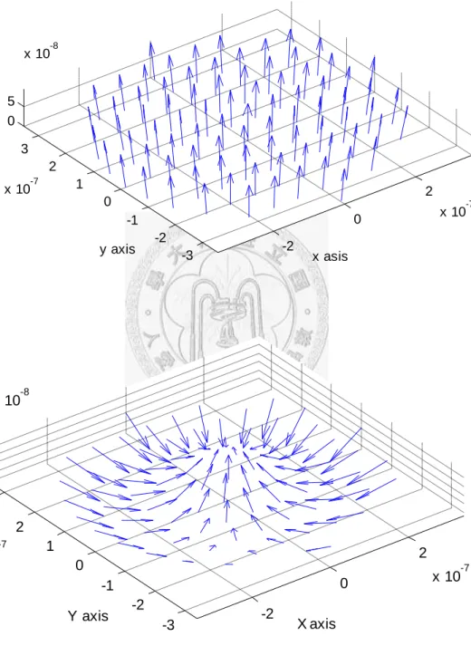
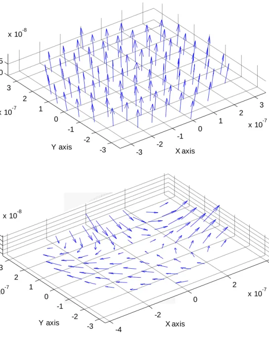
y dilatational modes.. ... 39 Fig. 4-6 Dispersion relation of a cylindrical waveguide of radius as 340nm and composed of SiO2. The red lines are from Pochhammer Chree theory, a standard solution for an isotropic waveguide. The blue circles are from RUS method. ... 41 Fig. 4-7 Displacement fields of (a) mode 1 and (b) mode 2of Pochhammer Chree theory. ... 42 Fig. 4-8 Displacement fields of (a) mode 1 and (b) mode 2 of RUS method ... 43Fig. 4-9 Displacement fields of (a) mode 3 and (b) mode 4 of RUS method ... 44 Fig. 4-10 Calculated dispersion relations of a 340nm-diameter GaAs nanorod. The red dot is calculated from Pochhammer Chree equation, and the solid blue line is calculated from RUS method. ... 46 Fig. 5-1 Transient change in reflectivity of the sample induced by the pump beam (880nm). A small oscillatory signal that is attributed to coherent phonon generation of the sample is highlighted in the figure. The inset shows the full measured trace. ... 49 Fig. 5-2 Frequency spectra of 340nm-diameter nanorod samples. ... 52 Fig. 5-3 Size dependency of the dominating frequency under 880nm probe used ... 52 Fig. 5-4 Transient reflectivity change traces of different sample of different diameter and period under 1120nm probe used ... 53 Fig. 5-5 Transient reflectivity change of the sample of 239nm-diameter and 355nm-period for (a) infrared (1120nm) probe and (b) near-infrared (880nm) probe. (each trace was normalized by its minimum value) ... 54 Fig. 5-6 (a) Background-substration oscillatory signal of the sample of 256nm diameter and 355nm period. (b) The signal of the sample of 239nm-diameter and 355nm-period. ... 55 Fig. 5-7 Frequency spectra of the signal at different timeframe: Black line is full oscillatory signal, red line is that of initial oscillation, and blue line is that of echo signal. (a) The signal of the sample of 255nm-diameter and 355nm-period. (b) The signal of the sample of 239nm-diameter and 355nm-period. Note: Zero padding was used to make the length of each data equal to fairly compare ... 56 Fig. 5-8 Frequency spectra of the signal of the sample of 180nm diameter for 880nm
probe (black-square line) and 1120nm probe (red-circle line). The dominating peak in red-circle line represents the radial breathing mode of GaAs nanorods. ... 57 Fig. 5-9 Frequency spectra of the signal of the sample of 250nm diameter for each 880nm probe (black-square line) and 1120nm probe (red-circle line). The dominating peak in red-circle line represents the radial breathing mode of GaAs nanorods. ... 57 Fig. 5-10 Dominating frequency versus the diameter of the rod under 1120nm probe.58 Fig. 5-11 The measured trace of transient change in reflectivity of the sample of
256nm diameter and 355nm period.(The frequency of the oscillation highlighted is around 52GHz) ... 59 Fig. 5-12 (a) SEM image of the Au-attached GaAs nanorods. In this figure the thickness of metal layer can be identified as ~27nm. The graph is taken by Hung-Pin Chen who is a member of our group. (b) Schematic diagram of lateral and thickness vibration of a nanodisk. ... 60 Fig. 5-13 Dimensionless dispersion relation of an acoustic cylindrical waveguide
with infinite length (made of GaAs). The horizontal dashed line represents the dimensionless excitation induced by the lateral vibration of the Au nanodisk. ... 63 Fig. 5-14 Displacement field distribution of excited guided modes (Mode 1). (The pattern is drawn at the crossing points in the dispersion curve which is shown in Fig. 5-13.) ... 65 Fig. 5-15 Displacement field distribution of excited guided modes (Mode 1). (The pattern is drawn at the crossing points in the dispersion curve which is shown in Fig. 5-13.) ... 66
Fig. 5-16 Simulation of the excited wave packet propagation by considering the dispersive behavior of the fundamental guided mode (mode 1). (The
simulation does not consider any loss.) ... 66
Fig. 5-17 Simulation of the single and the double roundtrip echo. (The simulation does not consider any loss for the echos.) ... 67
Fig. 5-18 Schematic diagram for the echoes observed in experiments... 68
Fig. 5-19 Fitted result of the data. (Diameter:231nm, period 355nm)... 70
Fig. 5-20 Fitted result of the data. (Diameter:273nm, period 355nm)... 70
Fig. 5-21 (a) Background-removed oscillatory signal of 273nm-diameter sample (probe:1120nm). (b) Corresponding frequency spectra of the signal and the noise. ... 73
Fig. 5-22 Schematic diagram of (a) the mode with major component in axial direction and (b) the mode with major component in radial direction ... 74
Fig. 5-23 Background-removed oscillatory signal of 440nm-diameter sample (probe:1120nm). (b) Corresponding frequency spectrum ... 75
Fig. 5-24 (a) Background-removed oscillatory signal of 340nm-diameter sample. (b) Corresponding frequency spectrum. (Probe:1120nm) ... 76
Fig. 5-25 Backward Brillouin oscillation induced by fundamental mode that satisfying the phase matching comditon ... 77
Fig. 5-26 Schematic diagram of explanation of the strength of the detected backward Brillouin oscillation signal ... 79
LIST OF TABLES
Table 2-1 Detailed information of samples used in this thesis ... 11 Table 4-1 Classification of normal modes ... 39
Chapter 1 Introduction
1.1 Picosecond Ultrasonic (Nano-Acoustic Waves)
Picosecond ultrasonic for its wide applications in physics and engineering has attracted many attentions in recent years. From the first paper reported in 1984, C.
Thomsen et al. [1.7] discovered the extremely short time (~ps) oscillation in transient change of transmission and reflection of probe light when the picosecond pump-probe experiment was conducted on thin films of
a As Te
2 3 and cis-polyacetylene( CH )
x. They attributed the observed oscillations to the generation and the propagation of GHz coherent acoustic phonons which perturb the optical properties of the sample, and they developed a physical model to interpret the mechanisms of generation and detection of coherent acoustic phonon in a later paper [1.6] in 1986.In a conventional pulsed ultrasonic system, a coherent acoustic pulse is generated by the application of an electric pulse to a suitable transducer, in such an experiment the time resolution is limited by the overall bandwidth of the system. This bandwidth is determined by the mechanical characteristics of the transducer and the electric bandwidths of the generating and the receiving system. The limited time resolution of the system has been proven to be the level of nanosecond (10 sec9 ), however it is still clearly inadequate to study the character of nanostructures for its limited spatial resolution (several microns). Unlike the conventional ultrasonic system, picosecond ultrasonic technique exhibits the nano-resolution ability in space for the acoustic pulses generated with very short spatial extent around 10nm~100nm (therefore it is also called nano-acoustic waves (NAWs) [1.16]) and for the high resolution in time scale of the femtosecond laser system. This technique was mostly used for nondestructive detection evaluation (NDE) in nanostructures, like thickness estimation of an ultra-thin films by
measuring arrival time of returning echoes [1.4][1.10] and bonding evaluation of interfacial surfaces [1.2] due to a lower transmissivity of acoustic energy for a poor bonding, and so on. In fundamental physics, the generation and the propagation of NAWs are closely related to mechanical and physical properties of nanostructures [1.1]
and nanodevices, therefore the studies like sound velocity measurement [1.10], the attenuation measurement of high frequency phonon [1.8][1.9], phonon-carrier interaction, and carrier diffusion [1.11] have been investigated on several semiconductors and metals.
With the increasing investigation and developments of NAWs, it actually provides researchers and scientists a powerful tool on the study of nano-device physic and novel implementation of nano-engineering.
1.2 Femtosecond Pump-Probe Technique
The continuous improvement in ultrafast laser technology have led to many new and fascinating applications in physics, engineering, chemistry, and biology. With these progresses, ultra-short laser pulse width well below 1 picosecond has been achieved.
One of these applications is ultrafast pump-probe technique, which is widely used to study the ultrafast phenomenon in semiconductors and metals, such as carrier dynamic [1.18][1.19] and coherent GHz~THz acoustic phonons effect.
Fig. 1-1 shows the schematic diagram of a typical femtosecond pump-probe system. An optical pulse with its width well below 1ps is generated by a femtosecond laser, and then it is divided into two beams for different purposes: the sample is excited by one pulse (pump beam), whereas the transient changes of the sample induced by the pump beam are probed by the other pulse (probe beam). The time delay between pump
and probe is controlled by a delay stage which provides variable optical path difference, thus the transient optical properties change of the sample at different time delays can be recorded with the time scale shorter than 1ps. In the past studies [1.6][1.20][1.21], the ultrafast pump-probe technique has been proven to be a efficient way to generate and detect GHz~THz coherent acoustic phonons in many materials. Therefore, in this thesis, a two-color pump-probe experiment was employed to study ultrafast acoustic responses of the designed samples and to investigate coherent acoustic waves which are generated and guided in GaAs noanrods.
Fig. 1-1 Schematic diagram of a femtosecond pump-probe experiment
1.3 Motivation
In the view of wave propagation, a finite solid structure, like a rod or a plate, can be viewed as a waveguide that directs acoustic waves to propagate toward a specific direction. Dispersive behavior and field distribution of discrete guided modes are quite different as compared to plane waves in a bulk crystal. However, in previous studies, owing to the spot size (~20
m
) of focused optical pulses (pump) is much greater thanthe optical absorption depth (~10nm), the excited acoustic waves were treated like that propagate inside a bulk crystal without seeing the boundary (for the lateral size of sample was usually much greater than the spot of NAWs) and diffraction (near field approximation for less than few
m
propagation distance), thus the guided effect was neglected and the propagation could be simply modeled as a 1D problem. On the other hand, despite the confined acoustic modes of nanostructures are reported, such as nanodot [1.25], nanorod[1.3][1.22], nanoprism[1.23], nanobshell[1.23] and nanocubes [1.24], how the acoustic waves propagate within the nanostructure has not been revealed.Recently, one-dimensional materials such as nanowires have attracted considerable attention due to their potential application in energy conversion devices. When crystalline solids are confined to nanometer range, phonon transport within them would be significantly altered due to various effects, namely (1) increased boundary scattering, and (2) modification on phonon dispersion relation. Theoretical studies have suggested that, as the wire diameter is smaller than the phonon mean free path (MFP), the dispersion relation should be modified due to the confinement, for example the phonon group velocity would be significantly less than that in bulk.
Furthermore, when the phonon transport fall into ballistic regime, the thermal conductivity exhibits the quantization. Under this scheme, the wave’s properties that are treated as guided waves in these low-dimensional nanostructures are necessary to be taken into consideration. A lot of theoretical studies have calculated the transmission properties of guided modes at the abrupt junction and proposed that thermal conductance could be modified by the shape discontinuity. However, the related experimental work has not been reported as well.
In the low temperature limit, thermal transport are dominated by the lowest
acoustic modes, this frequency range (GHz to sub THz) can be achieved by the usage of picoseconds ultrasonic techniques. Therefore, the study of guided NAWs might provide another viewpoint to investigate the novel thermal properties between low-dimensional structures.
In addition, the dispersive effect resulted from lateral confinement is relatively significant. This makes investigation possible on picosecond nonlinear acoustics, i.e.
acoustic soliton, a wave packet propagates with stationary shape in space and a constant velocity for the balance between nonlinearity and dispersive effects [1.12].
Finally, as an analogy to optical systems, the developed bulk NAWs systems so far still lacks an important component: waveguide. Therefore, we proposed the nanorod to serve as a candidate for waveguide utility in nano-ultrasonic imaging, sensing, and other nano-acoustic devices.
Being the first stage of these aims, the investigation of guided NAWs in a nanorod is necessary and impotant. Therefore it is studied and discussed in this thesis.
1.4 Thesis Structure
In this thesis, we studied the guided NAWs confined to a GaAs nanorod by the usage of two-color femtosecond pump probe technique that excites and detects NAWs in our designed samples. Time-resolved oscillations observed in experiments are discussed and compared with an anisotropic waveguide theory of continuum elasticity and other possible acoustic responses of the designed samples. The thesis is organized as follows:
To understand the nature of signal observed, rod size and probe wavelength are controlled as variables in the experiments. Therefore, Chapter 2 gives the information
about designed samples and the detail of two experimental setups used for different probe wavelength with respect to near infrared (880nm) and infrared (1120nm) region.
In Chapter 3, the author described some other possible acoustic dynamical responses that has been found to play a role in the nanorod array samples. For quantitative elucidation to guided NAWs, Chapter 4 introduces continuum elastic waveguide theory of infinite isotropic and anisotropic cylindrical rods.
Chapter 5 gives the experimental results and discussion. It was divided into two parts according to the used probe wavelength. For these different cases, different oscillatory signals and the echoes formed by guided modes were observed. Finally, summary and future work of this work are given in the last chapter of this thesis.
Reference
[1.1] B. Bonello, B. Perrin, E. Romatet, J.C. Jeannet, ―Application of the picoseconds ultrasonic technique to the study of elastic and time-resolved thermal properties of materials‖ Ultrasonic, 35, 223 (1997).
[1.2] G. Tas, J.J. Loomis, H.J. Maris, A.A. Balies and L.E. Seiberling. ―Picosecond ultrasonics study of the modification of interfacial bonding by ion implantation.‖
Appl. Phys. Lett. 72. 2235 (1998).
[1.3] M. Hu, X. Wang, G. Hartland, P. Mulvaney, J. Juste, and J. Saders, ―Vibrational response of nanorods to ultrafast laser induced heating: Theoretical and experimental analysis,‖ J. Am. Chem. Soc, 125, 14925 (2003).
[1.4] H.N. Lin, R.J. Stoner, H.J. Maris, ―Nondestructive testing of microstructures by picosecond ultrsonics,‖ J. Nondestruct. Eval. 9, 239 (1990).
[1.5] G.A. Antonelli and H.J. Maris, S.G. Malhotra and James M.E. Harper,
―Picosecond ultrasonic study of the vibrational modes of a nanostructure,‖ J. Appl.
Phys., 91, 3261 (2002).
[1.6] C. Thomsen, H. T. Grahn, H.J. Maris and J. Tauc, ―Surface generation and detection of photons by picoseconds light pulses,‖ Phys. Rev. B., 34, 4129 (1986.) [1.7] C. Thomsen, J. Strait, Z. Vardeny, H.J. Maris and J. Tauc, ―Coherent phonon
generation and detection by picoseconds light pulses,‖ Phys. Rev. Lett., 53, 989 (1984).
[1.8] T.C. Zhu, H.J. Maris, and J. Tauc, ―Attenuation of longitudinal-acoustic phonons in amorphous SiO2 at frequencies up to 440GHz,‖ Phys. Rev. B., 44, 4281
(1991).
[1.9] H.N. Lin, R.J. Stoner, H.J. Maris and J. Tauc, ―Phonon attenuation and velocity measurements in transparent materials by picoseconds acoustic interferometry,‖
J. Appl. Phys, 69, 3816 (1990).
[1.10] O.B. Wright, ―Thickness and sound velocity measurement in thin transparent films with laser picoseconds acoustics,‖ J. Appl. Phys, 71, 1617 (1992).
[1.11] O.B. Wright, ―Ultrafast nonequilibrium stress generation in gold and silver,‖
Phys. Rev. B., 49, 9985 (1994).
[1.12] H.Y. Hao and H.J. Maris, ―Experiments with acoustic solitons in crystalline solids,‖ Phys. Rev. B., 64, 064302 (2001).
[1.13] G. Tas and H.J. Maris, ―Picosecond ultrasonic study of phonon reflection from solid-liquid interfaces,‖ Phys. Rev. B., 55 1852 (1997).
[1.14] X.F. Peng, K.Q. Chen, B.S. Zou and Y. Zhang, ―Ballistic thermal conductance in a three dimensional quantum wire modulated with the stub structure.‖ Appl.
Phys. Lett., 90, 193502 (2007).
[1.15] Y.C. Wen, J.H. Sun, C. Dais, D. Grutzmacher, T.T. Wu, J.W. Shi, and C.K. Sun,
―Three-dimesional phononic nanocrystal composed of ordered quantum dots.‖
Appl. Phys. Lett., 96, 123113 (2010).
[1.16] K.H. Lin, C.M. Lai, C.C Pai, J.I. Chyi, J.W. Shi, S.Z. Sun, C.F. Chang and C.K.
Sun, ―Spatial manipulation of nanoacoustic waves with nanoscale spot sizes,‖
Nature Nanotech., 2, 704 (2007).
[1.17] Y.H. Chen. ―Coherent Opto-Acoustic Behaviors of GaAs Nanorods‖ Master Thesis, (2009).
[1.18] C. Shank, R. Fork, R. Leheny, and J. Shah, "Dynamics of photoexcited GaAs band-edge absorption with subpicosecond resolution," Phys. Rev. Lett., 42, 112 (1979).
[1.19] D. Kim and P. Yu, "Hot-electron relaxations and hot phonons in GaAs studied by subpicosecond raman scattering," Phys. Rev. B, 43, 4158 (1991).
[1.20] S. Wu, P. Geiser, J. Jun, J. Karpinski, and R. Sobolewski, "Femtosecond optical generation and detection of coherent acoustic phonons in GaN single crystals,"
Phys. Rev. B, 76, 85210 (2007).
[1.21] C.K. Sun, J.C. Liang, and X.Y. Yu, "Coherent acoustic phonon oscillations in semiconductor multiple quantum wells with piezoelectric fields," Phys. Rev.
Lett., 84, 179 (2000).
[1.22] S.O. Mariager, D.K. Khakhulin, H. T. Lemke, K.S. Kjar, L. Guerin, L. Nuccio, C.B. Sorensen and M.M. Nielsen and R. Feidenhans’l, ―Direct observation of acoustic oscillations in InAs Nanowires,‖ Nano. Lett., 10, 2461-2465 (2010).
[1.23] P. Yu, J. Tang, and S. H. Lin, "Photoinduced structural dynamics in laser-heated nanomaterials of various shapes and sizes," The Journal of Physical Chemistry C, 113, 7480 (2009).
[1.24] H. Petrova, C.H. Lin, S. de Liejer, M. Hu, J.M. Mclellan, A.R. Siekkinen, B.J.
Wiley. M. Marquez, Y. Xia, J.E. Sader, G.V. Hartland, "Time-resolved spectroscopy of silver nanocubes: observation and assignment of coherently excited vibrational modes," J. Am. Chem. Soc., 126, 094709 (2007).
[1.25] T.D. Kruss and F.W. Wise. ―Coherent acoustic phonon in a semiconductor quantum dot.‖ Phys. Rev. Lett., 79, 5102-5105 (1997).
Chapter 2 Designed Sample and Experimental Setup
2.1 Designed Structure of Samples
To study guided NAWs in the nanorod, the source of generation of NAWs is needed.
Therefore, we would like to briefly introduce the generation mechanisms here and then give the reason why the structure of sample was designed.
From the past abundant researches and studies, the ways to generate NAWs in metals and semiconductors by optical excitation can be roughly classified as below:
(1) Thermal stress [2.1]: the optical-absorbing region suffers instant thermal expansion due to rapid temperature rise resulted from strong absorption of femtosecond light pulses, and thus launch acoustic waves outward.
(2) Deformation potential [2.1][2.2]: it is one of dominating mechanisms for phonon generation in semiconductors. Since the generation of electron-hole pairs excited by optical pulses would introduce an electronic stress to perturb equilibrium status of the lattice. (Valance band electrons in general help to bind the lattice more effectively than the conduction electrons)
(3) Piezoelectric effect: it has been reported to be an efficient way to generate high-amplitude coherent sub-THz phonon compared to the other mechanisms [2.4]. By using highly strained quantum well structures, NAWs are generated via piezoelectricity for excited electrons and holes are separated by original built-in electric field, and then introduce an additional field that perturbs the equilibrium status of lattices. This technique has been used for manipulation of NAWs pulse shape and frequency spectrum [2.4], etc.
For these mechanisms discussed above, the simplest way to generate NAWs in the nanorod is thermal stress. A metallic film of nano-thickness was proposed to be used as
a better transducer for its high optical absorption that can increase temperature rise [2.5].
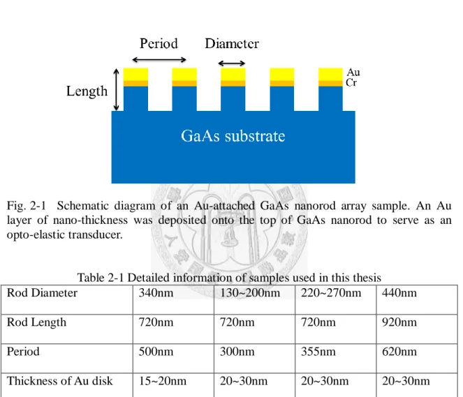
Therefore, for our samples, an Au layer of nano-thickness was designed to deposit onto the top of the GaAs nanorod to serve as an opto-elastic transducer.
The schematic diagram is given in Fig. 2-1. Detailed information of designed samples used in this thesis is arranged as the following:
Fig. 2-1 Schematic diagram of an Au-attached GaAs nanorod array sample. An Au layer of nano-thickness was deposited onto the top of GaAs nanorod to serve as an opto-elastic transducer.
Table 2-1 Detailed information of samples used in this thesis
Rod Diameter 340nm 130~200nm 220~270nm 440nm
Rod Length 720nm 720nm 720nm 920nm
Period 500nm 300nm 355nm 620nm
Thickness of Au disk 15~20nm 20~30nm 20~30nm 20~30nm
The samples were provided by Prof. Min-Hsiung Shih (Research Center for Applied Sciences, Academia Sinica). Among these samples, the one of 340nm diameter was grown by Cheng-Wen Cheng, and the other samples were grown by Hsiang-Yu Chou, both are members in Prof. Shih’s group. The growing process of these two sets of sample are slightly different while the latter modified the process to better control the
thickness of Au layer and to reduce the over-deposited Au that attaches on the side wall and the bottom of nanorods.
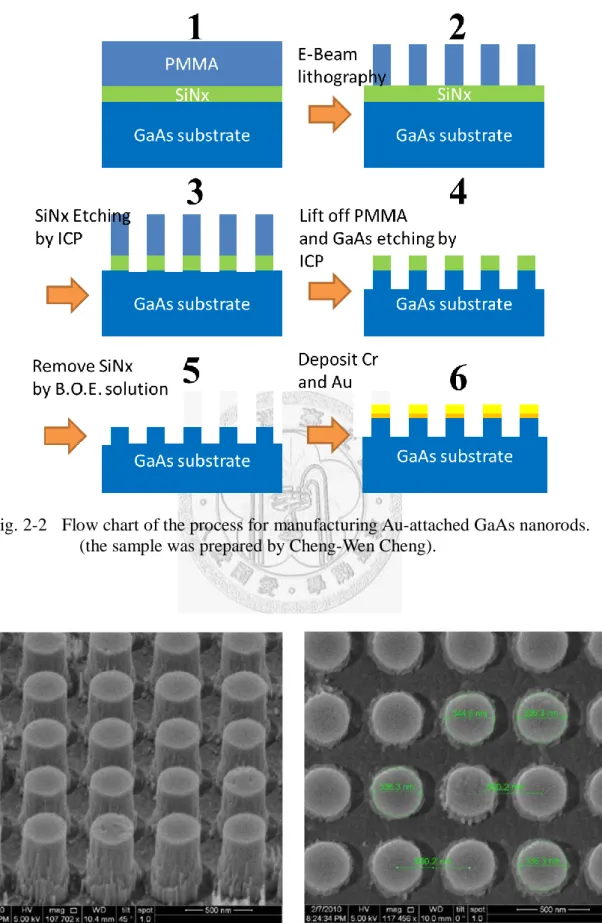
Fig. 2-2 shows the flow chart of sample processing for the 340nm-diameter sample.
First, a SiNX film was deposited on a [100] GaAs wafer by MOCVD (Metal-Organic Chemical Vapor Deposition) and spin coated PMMA (Poly(methyl methacrylate)) on the SiNX film. Second, use EBL (E-Beam Lithography) to write the patterns of nanorods.
After the development, the patterned PMMA film acted as a mask for the SiNX film.
Third, etch the SiNX film by ICP (Inductively Coupled Plasma). Fourth, lift off the PMMA film and now the patterned SiNX film acted as a mask for the GaAs wafer, and then etched the GaAs wafer by ICP again. Finally, remove the SiNX by the B.O.E solution and deposited chromium and gold onto the sample.
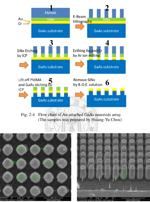
For the other samples (samples of diameter that are below 300nm and the one of 440nm diameter), the processing is briefly described in Fig. 2-3. The main differences from the former are the pre-deposited Cr (~5nm) and Au layer on the GaAs wafer. Then, the PECVD (Plasma-enhanced Chemical Vapor Deposition) was used to deposit the SiNx onto it, and followed by PMMA layer by spin coating. The remaining processes are the same as the former except an additional step to etch the Cr and the Au by Ar ion milling. Since the Au layer was deposited at first on the GaAs wafer, the homogeneity of deposited Au layer could control better and the over-deposition could be avoided as well.
Fig. 2-2 Flow chart of the process for manufacturing Au-attached GaAs nanorods.
(the sample was prepared by Cheng-Wen Cheng).
Fig. 2-3 SEM image of the Au-attached GaAs nanorods array. (a) Side view of the nanorods, the height of the rods is ~720nm from the image, and (b) top view of the nanorods, the diameter is around 340nm from the image.
Fig. 2-4 Flow chart of Au-attached GaAs nanorods array.
(The samples was prepared by Hsiang-Yu Chou)
Fig. 2-5 SEM image of the Au-attached GaAs nanorods array. (a) Top view of GaAs nanorod, the diameter is around 256nm, and the period is 355nm from the image. (b) Side view, the height is ~ 720nm. (The sample was made by Hsiang-Yu Chou, and the SEM images were taken by Hung-Ping Chen.)
2.2 Experiment Setup
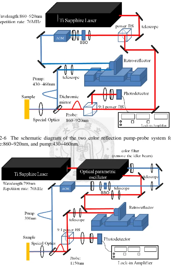
A two-color reflection pump-probe system was used to study the acoustic dynamic response of Au-attached GaAs nanorods array. Transient change of reflectivity induced by the pump is recorded by the following probe. A wavelength-tunable femtosecond mode-locked Ti:Sapphire laser (Coherent Mira 900) was used to generate laser pulses with its pulse width ~200 femtosecond (1015sec) and a repetition rate of 76MHz. Due to the demand for different probe wavelengths, two experimental setups were employed with respect to the near infrared (880nm) and infrared region (1120nm). The author would give the details about these two experimental setups in the sections 2.2.1 and 2.2.2.
2.2.1 Experiment Setup (probe: 880nm, pump: 440nm)
In the wavelength range between 700nm to 1
m
, the femtosecond laser (Coherent Mira 900) was used to generated light pulses. The generated beam (880nm) was first separated into two beams by non-polarized power beam splitter, and one with higher power acts as the pump beam, and the other attenuated by a neutral density filter as the probe beam. For the two-color pump-probe system, the pump beam was first focused on a BBO crystal for the second harmonic generation (880nm440nm), and then it was directed to pass through a color filter to remove the component of fundamental frequency. The pump beam was then collimated and guided into a retro-reflector on a translation stage, which provided controllable optical path difference between the pump and the probe beam. To enhance signal-to-noise ratio (SNR), the pump beam was directed to pass through an acoustic-optic modulator (AOM), which modulate the beam with higher frequency (100 kHz~600 kHz) than the chopper (~1.5 kHz). The modulation frequency of the AOM was chosen for the smallest noise level in electronicsystem and always below 500 KHz.
On the other hand, we used a set of telescope to control the divergence of the pump beam so that two beams with different wavelengths can focus on the same focal plane. A lens was used to focus both beams to achieve small spot-size that can be fully located within the nanorod pattern. Moreover, before both beam were focused, they were overlapped collinearly by using a dichroic mirror. In addition, the input power of the pump beam was set to prevent the sample from damage.
The reflection of probe beam was then collected and focused onto the photo-detector through a color filter which effectively removed the scattered pump. Finally, the output signal of the photo-detector was connected to a RF lock-in amplifier (Stanford Research SR-844) which was locked with the same modulation signal of the AOM. The small pump-induced signal was extracted from noise by the RF lock-in amplifier since the modulated pump resulted in a variation of reflection of the probe at the same modulation frequency. We then recorded and averaged the measured traces in a computer as a function of time delay between the pump and the probe beam. Fig. 2-6 shows the schematic diagram of the pump-probe system set up.
2.2.2 Experiment Setup (probe: 1120nm, pump: 390nm)
The wavelength of probe was chosen to be longer to study wavelength dependency of acoustic responses of the samples. Due to the limited wavelength output from the femtosecond Ti-Sapphire laser (700-1000nm), the optical parametric oscillator (OPO) was employed to generate the probe of wavelength above 1
m
. Femtosecond light pulses with central wavelength of 780nm from the Ti-Sapphire laser were used to pump the OPO, and then the optical parametric down conversion process converted the input beam into two outputs: the ―signal‖ and the ―idler‖. Signal beam is defined by the higher frequency (short wavelength) of the two generated outputs. According to the working principle (nonlinear process) of OPO, signal beam of 1120nm wavelength that was used to probe the samples will be generated. In order to remain the same excitation condition for the sample as possible, the ultraviolet pump is demanded. Therefore the idler beam was filtered and remaining unconverted pumping beam (790nm) was output from OPO cavity and focused onto the BBO crystal to double the frequency (790nm→390nm), and then it was used as the pump beam to excite the samples. The different optical path between the pump and the probe beam within the OPO cavity was calculated and compensated in the outside-cavity optical path. Three sets of telescopes were settled in the experiment. Two of them was installed to collimate the two highly-divergent beams when output from the OPO cavity and the other is used to adjust the focal depth of the pump to match the probe beam. The remaining details are the same as previous setup, and the schematic diagram of the system setup is given in Fig.
2-7.
Fig. 2-6 The schematic diagram of the two color reflection pump-probe system for probe:860~920nm, and pump:430~460nm.
Fig. 2-7 The schematic diagram of the two color reflection pump-probe system for probe:1150nm (from OPO), and pump:390nm (from tunable modelock Ti-sapphire laser).
Reference
[2.1] C. Thomsen, H. T. Grahn, H.J. Maris and J. Tauc, ―Surface generation and detection of photons by picoseconds light pulses,‖ Phys. Rev. B., 34, 4129 (1986.) [2.2] O. Matsuda, T. Tachizaki, T. Fukui, J.J. Bauberg and O.B. Wright, ― Acoustic phonon generation and detecton in
GaAs
/Al Ga As
0.3 0.7 quantum wells with picoseconds laser pulse.‖ Phys. Rev. B., 71, 115330 (2005)[2.3] P. Babilotte, P. Ruello, T. Pezeril, G. Vaudel, D. Mounier, J.-M. Breteau and V.
Gusev. ― Transition from piezoelectric to deformation potential mechanism of hypersound phtogeneration in n-doped GaAs semiconductors.‖ J. Appl. Phys, 109, 064909 (2011).
[2.4] C.K. Sun, J.C. Liang, X.Y. Yu. "Coherent Acoustic Phonon Oscillations in Semiconductor Multiple Quantum Wells with Piezoelectric Fields." Physical
Review Letters 84(1): 179. (2000)
[2.5] H.N. Lin, R.J. Stoner, H.J. Maris, ―Nondestructive testing of microstructures by picosecond ultrsonics,‖ J. Nondestruct. Eval. 9, 239 (1990).
[2.6] C. T. Yu, K.H. Lin, C.H. Hsieh, C.C. Pan, J.I. Chyi and C.K. Sun. ―Generation of frequency-tunable nanoacoustic waves by optical coherent control.‖ Appl. Phys.
Lett., 87, 093114 (2005)
Chapter 3 Acoustic Dynamics of Laser-Heated Periodic Nanorod Structures
Despite our samples were designed to study the guided NAWs in the GaAs nanorod, however, from the abundant pump-probe studies about picosecond ultrasonics of periodical nanostructures, we were well aware that there are many mechanisms which would play a role in the present experimental scheme. Therefore this chapter would like to introduce possible acoustic dynamic responses of the periodic Au-attached GaAs nanorod array samples. These mechanisms have been well studied on individual or periodical nanostructures which are similar to our scheme. In the following, mechanisms about breathing mode vibration of a nanorod, surface acoustic waves (SAWs) in surface-patterned structures, backward Brillouin oscillation (interferences between the original reflected probe and an additional one induced by the propagating strain), and acoustic modes of metallic nano-objects would be introduced in detailed.
3.1 Radial Breathing Mode of Nanorods
A number of groups have shown that ultrafast laser excitation of nanoparticles can coherently excite low frequency vibration modes [3.1]. For semiconductors, the above-bandgap excitation changes the dimensions of the unit cell, which can impulsively excite totally symmetric phonon modes (vibrational modes). Symmetric breathing modes possess the nature of being most possibly excited for homogenous optical illumination excitation scheme. Observations of radial breathing modes of slender nanorods ( /
l a
1) of metals and semiconductors have been reported in some literatures [3.4][3.5]. Fig. 3-1 shows the displacement pattern of the radial breathingmode of a rod, a pure expansion and contraction in radial is observed. The detailed mathematical derivation can be found elsewhere [3.4], thus here we only emphasize the assumptions of the model and its analytical result. The natural resonant frequency of the fundamental radial breathing mode of a rod is given by the following formula [3.4]:
(1 )
2 (1 )(1 2 ) 2
L br
V
E v
f a v v a
, (3.1)where
a
is the radius of the rod, E is Young modulus,v
is Poisson ratio,
is the mass density,V
L is the longitudinal velocity, and the parameter
is the fundamentalsolution of the eigenvalue equation: 0
( ) 1 2
1( ) 1
J v J
v
[3.4] (J
0 andJ
1 are the zero and the first order Bessel function of first kind, respectively.)Fig. 3-1 Displacement field of radial breathing mode of a nanorod. Pure radial expansion and contraction is observed. (Reprinted with permission from [3.4].
Copyright 2010 American Chemical Society.)
The model is based on the assumptions of isotropic material and a free cylinder with a high aspect ratio (thus the boundary conditions at the end surfaces can be reasonably ignored). In the present case, although nanorods do stand upon the substrate, which should modify the boundary conditions of the surface, in reference [3.5], Simon O. Mariager et al. has showed the detection of radial breathing mode of InAs nanowires under the pump-probe experimental scheme.
3.2 Surface Acoustic Waves in Surface-Patterned Structures
In a semi-infinite solid, surface acoustic waves (SAWs) is a type of acoustic waves propagating along the surface of an elastic medium. The waves have its amplitude that typically exponentially decays with depth into the substrate and the slower velocity than the body waves. Since a periodic structure provides spatial modulation in surface, SAWs can be excited in a sample with grating or periodic patterns which are fabricated on the surface. D. H. Hurley et al. [3.6] showed the excitation and detection of SAWs of nano-wavelength in a 1D sub-optical wavelength grating structure under the pump-probe experimental scheme. Furthermore, J. F. Robillard et al. [3.7] revealed that there are two kinds of vibration modes in 2D periodic nanocubes: (1) individual resonance modes of a nanocube, and (2) collective modes which represent the coupling between the cubes of the artificial 2D lattice (phononic crystal). The collective modes exhibit strong dependency on the spacing period and possess the dispersive nature of SAWs as the periodic spacing becomes infinite. The frequencies of these surface acoustic modes can be formulated with the Rayleigh wave velocity
V
R [3.8] as:2 2
2
,R R
i j
V V
f k i j
a
, (3.2)where
a
is the spacing (periodicity), and ( , )i j are integers which represent the wave
vectors in a reciprocal lattice. In addition, the paper also reported a phenomenological condition for being able to detect these modes: the probe wavelength is close to or smaller than the periodic spacing of the nanostructure, i.e.1
a
should be satisfied.
Fig. 3-2 Schematic diagram of SAWs in the periodic surface-patterned structure.
3.3 Backward Brillouin Oscillations
Acoustic disturbance can modulate optical properties of material via the photoelastic effect, which is a phenomenological description of the change of permittivity with a relation of
p
, where ( n i )
2,p
is the photoelastic tensor and
is the strain field. Backward Brillouin oscillation is one of optical detection methods for propagating strain field. This mechanism can be understood by considering an acoustic wave as a moving mirror to induce an additional reflected probe [3.9][3.10]. As the acoustic wave propagates, constructive or destructive interference between the original reflected probe and the strain-induced reflected one would alternatively occur, depending on the distance that acoustic wave travels. Thus it makes the transient oscillation in reflectivity of probe with respect to the delayed time.However, an acoustic pulse is a combination of broad band frequency components, not all the acoustic component can be detected via this mechanism. According to the developed theoretical model [3.9][3.10], only the component which satisfies the ―phase matching‖ can contribute the signal. The condition is given as follows:
0
2 2 4
pr
q nk k n
, (3.3)where
q
,k
0, and k are the wave vectors of the acoustic component, the probe lightin vacuum, and the probe light in the sample, respectively.
n
is the refractive index, and
pr is the optical wavelength of the probe in vacuum. The frequency of backward Brillouin oscillation in transient reflectivity contributed by the acoustic component is [3.9]2 0
0
2 2
a q nk
nV
phf
, (3.4)where
V
ph is the phase velocity of the acoustic component, i.e.V
ph aq
. Theschematic diagram is shown in Fig. 3-3.
Fig. 3-3 Schematic representation of backward Brillouin oscillation. The incident probe was drawn in oblique for clear illustration.
3.4 Vibration of Metallic Nano-objects
The optical excitation of vibration modes of metallic nano-objects is slightly different to that of semiconductors. In metals, electrons are excited by absorbing optical pulses, and then quickly release their excess energy to the lattice via the electron-phonon coupling in the following picosecond interval. The process thereby
raises the lattice temperature and sets up the thermal stress. In the present sample, the Au nanodisk is expected to be the strongest absorbing part respect to the pump light in the structure, so it could possibly show the response of individual vibration of the nanodisk in the measurement.
Since the shape and the geometry of an object strongly affect its resonant modes, the mode of a thin film and a nanodisk are absolutely different. In the previous studies, typical generation mechanism used a metallic film of nano-thickness as a transducer [3.11][3.12]. Since the film can be viewed as an infinite extent as compared with its thickness, the vibration induced by the thermal expansion of small heated area can be viewed as a 1D problem, as shown in Fig. 3-4. The frequency of thickness vibration can be higher than hundreds of GHz due to successive reflections of acoustic waves at the thickness boundary [3.13]. Therefore the frequency can be simply determined from the formula:
2 V
Lf d
, (3.5)where d is the thickness of the film, and
V
Lis the longitudinal velocity in the thickness direction. However, the shape of the transducer used in our case was a disk rather than a film, the characteristic vibration mode is thus different than predicted one of the film. In the previous research, P. Yu et al. [3.14] has investigated the photo-induced structure dynamics of laser-heated metal nanodisks, in which they revealed that under the uniformly heating throughout the disk, the dominant mode that was excited should be the radial mode, and its frequency now depends on its radius rather than thickness. The frequency can be simply determined by:2 V
Lf D
, (3.6)where D is the diameter of the disk, and
V
Lis the longitudinal velocity in the radial direction. The schematic diagram is shown in Fig. 3-5.Fig. 3-4 Schematic diagram of generation of NAWs induced from the thickness vibration of metal thin film.
Fig. 3-5 Schematic diagram for radial vibration of Au nanodisk induced by the illumination of pump beam. The disk is attached onto a GaAs nanorod.
Reference
[3.1] G.V. Hartland. ―Coherent Excitation of Vibration Modes in Metallic Nanoparticles.‖ Annu. Rev. Phys. Chem. 57, 403 (2006).
[3.2] M. Yamaguchi, J. Liu, D. Ye, and T. M. Lu. ―Coherent acoustic vibration in silicon submicron spiral arrays.‖ J. Appl. Phys 106, 033517 (2009).
[3.3] A. Neleta, A. Cruta, A. Arboueta, N. Del. Fattia, F. Valléea, H. Portalèsb, L .Saviotc, E. Duvalb. ―Acoustic vibrations of metal nanoparticles: high order radial mode detection.‖ Appl. Surf. Sci. 226, 209 (2004).
[3.4] M. Hu, X. Wang, G. Hartland, P. Mulvaney, J. Juste, and J. Saders, ―Vibrational response of nanorods to ultrafast laser induced heating: Theoretical and experimental analysis,‖ J. Am. Chem. Soc, 125, 14925 (2003).
[3.5] S.O. Mariager, D.K. Khakhulin, H. T. Lemke, K.S. Kjar, L. Guerin, L. Nuccio, C.B. Sorensen and M.M. Nielsen and R. Feidenhans’l, ―Direct observation of acoustic oscillations in InAs Nanowires,‖ Nano. Lett., 10, 2461-2465 (2010).
[3.6] D. H. Hurley and K. L. Telschow. ―Picosecond surface acoustic waves using a suboptical wavelength absorption grating.‖ Phys. Rev. B, 66, 153301 (2002).
[3.7] J.-F. Robillard, A. Devos, and I. Roch-Jeune. ―Time-resolved vibrations of two-dimensional hypersonic phononic crystals.‖ Phys. Rev. B, 76, 092301 (2007) [3.8] J.-F. Robillard, A. Devos, I. Roch-Jeune, and P. A. Mante. ―Collective acoustic
modes in various two-dimensional crystals by ultrafast acoustics: Theory and experiment.‖ Phys. Rev. B, 78, 064302 (2008).
[3.9] C. Thomsen, H. T. Grahn, H. J. Maris and J. Tauc. ―Picosecond interferometeric technique for study of phonons in the brillouin frequency range.‖ Opt. Commun.,
60, 55 (1986)
[3.10] R. Liu, G.D. Sanders C.J. Stanton, C. S. Kim, J.S. Yahng, Y.D. Jho, K. J. Jho, K. J. Yee, E. Oh, and D. S. Kim. ―Femtosecond pump-probe spectroscopy of propagating coherent acoustic phonons in
In Ga
x 1xN GaN /
heterostructures.‖Phys. Rev. B., 72, 195335 (2005)
[3.11] A. Devos and R. Côte. ―Strong oscillations detected by picosecond ultrasonics in silicon: Evidence for an electronic-structure effect.‖ Phys. Rev. B., 70, 125208 (2004)
[3.12] Y. C. Wen, J. H. Sun, C. Dais, D. Grützmacher, T. T. Wu, J. W. Shi, and C. K.
Sun. ―Three-dimensional phononic nanocrystal composed of ordered quantum dots.‖ Appl. Phys. Lett. 96, 123113 (2010).
[3.13] H.N. Lin, R.J. Stoner, H.J. Maris and J. Tauc, ―Phonon attenuation and velocity measurements in transparent materials by picoseconds acoustic interferometry,‖ J. Appl. Phys, 69, 3816 (1990).
[3.14] Yu, P., J. Tang, et al. "Photoinduced Structural Dynamics in Laser-Heated Nanomaterials of Various Shapes and Sizes." The Journal of Physical Chemistry C
113(17): 7480-7480 (2009).
Chapter 4 Nano-Acoustic Guided Waves in Cylindrical Nanorods
4.1 Continuum Elastic Theory
Materials, such as solids, liquids and gases, are composed of atoms separated by empty space. However, macroscopic physical phenomena are usually modeled assuming the materials as a continuous medium, meaning the matter in the body is continuously distributed and fills the entire region of space it occupies. For the study of elastic behavior of solids, stress, expressed as force per unit area, is a measure of internal force of a deformable body. Strain, representing the deformation, is expressed as displacement per unit length. Both strain and stress are second rank tensors
ij ,
ij in the three-dimensional elasticity theory. Each tensor has 9 components for describing the normal and the shear parts. Constitutive equation,
ij C
ijkl
kl, known as a generalized form of Hooke’s law, describes the relation between stress and strain. The relation is governed by a fourth rank tensorC
ijkl(stiffness tensor) which is determined from the crystal properties.However, when the wavelength of acoustic waves becomes smaller than nano-scale and the frequency becomes higher than THz, the concept of energy quanta of vibration called phonons has to be introduced for quantum effect consideration. According to a simple model which places the equivalent springs between each atoms, as shown in Fig.
4-1, we can simply derive its dispersion relation [4.1] [4.4]. For a 1D diatomic model, phonons are classified into two types according to its different dispersive behaviors:
longitudinal acoustic (LA) and longitudinal optical (LO) phonons. For a more general 3D model, transverse phonons i.e. TA and TO, will be included. Dispersion curve of the
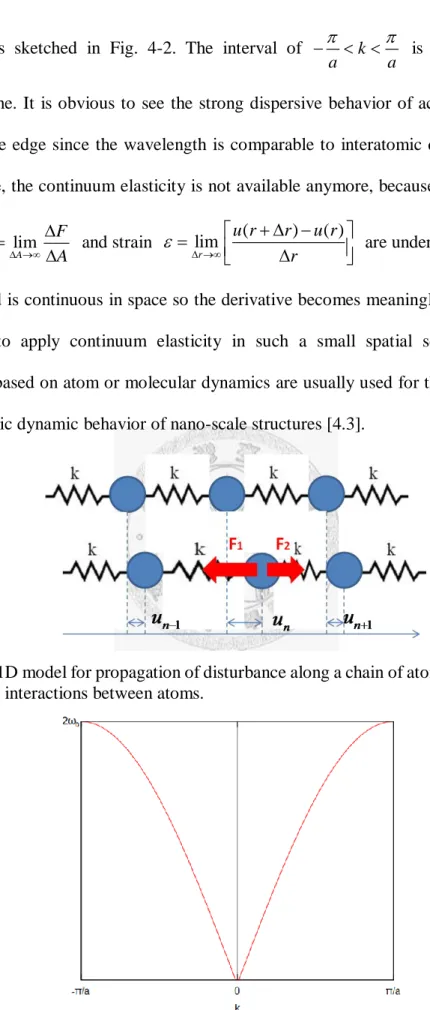
1D model is sketched in Fig. 4-2. The interval of
k
a a
is called the firstBrillouin zone. It is obvious to see the strong dispersive behavior of acoustic phonons near the zone edge since the wavelength is comparable to interatomic distance. In this extreme case, the continuum elasticity is not available anymore, because the definitions of stress
lim
A
F
A
and strain ( ) ( )lim
r
u r r u r
r
are under the assumptionthat the solid is continuous in space so the derivative becomes meaningless. Because of the failure to apply continuum elasticity in such a small spatial scale, numerical approaches based on atom or molecular dynamics are usually used for the investigation of the acoustic dynamic behavior of nano-scale structures [4.3].
Fig. 4-1 A 1D model for propagation of disturbance along a chain of atoms. The Springs represent the interactions between atoms.
Fig. 4-2 Dispersion relation of LA phonon for the 1D atom chain model, and a is the spacing between each atoms.
In this thesis, the central frequency of excited acoustic waves is around ten to hundred GHz and its wavelength is around ten nanometer or more. The fact means that the wave vector is still located near the center of the Brillouin zone, i.e. the acoustic wavelength is greater than several atom spacing. So the continuum linear elastic theory is still reasonably available and thus adopted in the following calculation.
4.2 Acoustic Waves in Bulk Crystals
In a bulk crystalline solid, which is often taken as an infinite medium, the waves are characterized by plane waves with three different polarization types. Christoffel’s equation and the slowness surfaces are useful to describe the velocities of (quasi-) longitudinal and (quasi-) transverse waves in any directions of space [4.4]. Fig. 4-3 shows the GaAs slowness surfaces in the (001) surface, in which it indicates the highly anisotropism and thus states the necessity of anisotropic waveguide model used in the following case.
Fig. 4-3 GaAs (cubic system) slowness surfaces (unit:
m
1) in the (001) surface. In the [100] and [010] direction, the corresponding velocities of quasi-longitudinal and quasi-transverse is 4731m/s and 3347m/s, respectively.4.3 Acoustic Waves in Finite Solid – Waveguide Theory
In a finite elastic object like a plate or a rod, acoustic waves would be reflected at the boundary. For satisfying the boundary conditions, the reflection of an oblique incident wave at the free surface must be accompanied with different wave type generated and reflected. For successive reflections at the surface, as shown in Fig. 4-4, it will totally form an overall lateral distribution and propagate toward the specific direction. This phenomenon leads to the idea of acoustic waveguides. Thus in the following, an isotropic and an anisotropic models will be introduced for qualitative elucidation of the phenomenon we observed experimentally.
Fig. 4-4 (a) Schematic diagram of successive reflections of acoustic waves at the free boundary, in which different wave type are represented by different color. (b) Overall lateral distribution that propagates toward the z direction
4.4 Acoustic Guided Waves in an Isotropic Cylindrical Rod
The problem of elastic wave propagation in an isotropic infinite solid cylinder was first developed by Pochhammer in 1876 and Chree in 1889 independently. The problem was treated based on three-dimensional elasticity and the full theory describes the propagation of axisymmetric, torsional, and flexural waves. Being as start to the waveguide theory and for the comparison to anisotropic cases, we will give a brief
![Fig. 4-3 GaAs (cubic system) slowness surfaces (unit: m 1 ) in the (001) surface. In the [100] and [010] direction, the corresponding velocities of quasi-longitudinal and quasi-transverse is 4731m/s and 3347m/s, respectively](https://thumb-ap.123doks.com/thumbv2/9libinfo/9598861.628531/48.892.296.610.530.1065/slowness-surfaces-direction-corresponding-velocities-longitudinal-transverse-respectively.webp)