Clock Skew Scheduling for Soft-Error-Tolerant Sequential Circuits*
Kai-Chiang Wu and Diana Marculescu
Department of Electrical and Computer EngineeringCarnegie Mellon University {kaichiaw, dianam}@ece.cmu.edu
Abstract
Soft errors have been a critical reliability concern in nano- scale integrated circuits, especially in sequential circuits where a latched error can be propagated for multiple clock cycles and affect more than one output, more than once. This paper presents an analytical methodology for enhancing the soft error tolerance of sequential circuits. By using clock skew scheduling, we propose to minimize the probability of unwanted transient pulses being latched and also prevent latched errors from propagating through sequential circuits repeatedly. The overall methodology is formu- lated as a piecewise linear programming problem whose optimal solution can be found by existing mixed integer linear program- ming solvers. Experiments reveal that 30-40% reduction in the soft error rate for a wide range of benchmarks can be achieved.
1. Introduction
Soft errors, process variations, and device aging phenomena are currently some of the main factors in reliability degradation.
With the continuous scaling of transistor dimensions, soft errors, which cause unpredictable transient circuit failure, are becoming increasingly dominant for functional reliability concerns [1]. A radiation-induced charged particle passing through a microelec- tronic device ionizes the material along its path and generates free pairs of electrons and holes. The free (ionized) carriers deposited around the particle track can be attracted or repelled by an internal electric field of the device and lead to an electrical pulse, referred to as a single-event transient (SET) or a glitch. A single-event upset (SEU) or a soft error refers to transient bit corruption that occurs when a single-event transient is large enough to flip the state of a storage node. The rate at which soft errors occur is called soft error rate (SER).
During SEU propagation in logic, three mechanisms used to provide logic circuits with effective protection against soft errors:
(i) logical masking, (ii) electrical masking, and (iii) latch- ing-window (timing) masking [2]. However, as technology scaling proceeds aggressively (e.g., decreasing node capacitance and increasing clock frequency), the impact of these three masking mechanisms is lessened. On the other hand, error detecting and correcting codes have been mature enough to successfully miti- gate soft error susceptibility of memory elements. A recent study [3] showed that soft errors significantly degrade the robustness of logic circuits, while the nominal SER of SRAMs tends to be nearly constant from 130nm to 65nm technologies. As a result, unless explicitly dealt with, the SER of logic will become as great of a concern and is expected to be comparable to that of unpro- tected memories by 2011 [4].
When the combinational block of a sequential circuit can propagate SETs freely, the sequential circuit may become very
* This research was supported in part by NSF Grant CNS-07020653.
sensitive to such events. This is because, once latched, soft errors can circulate through the circuit in subsequent clock cycles and affect more than one output, more than once. The untraceable propagation of soft errors greatly affects the circuit operation for consecutive cycles and thus, necessitates design methods for soft error tolerance of sequential circuits, in a similar manner to classic design constraints such as performance and power consumption.
In this paper, we present an analytical methodology for soft error tolerance of sequential circuits. Our work proposes to adjust the arrival times of clock signals to memory elements (latches or flip-flops) such that the probability of capturing unwanted tran- sient pulses is significantly decreased. The technique, called clock skew scheduling (CSS), is formulated in our methodology as a piecewise linear programming (PLP) problem, and its optimal solution can be found by existing mixed integer linear program- ming (MILP) solvers. The proposed framework involves only minor modifications of the clock tree synthesis step and does not touch the combinational logic of sequential circuits. Hence, this CSS-based approach can also act as a post-processing procedure for additional SER improvement on top of techniques targeting only combinational logic, which typically change the circuit timing and topology (e.g., resizing [5] and rewiring [6]).
The rest of this paper is organized as follows: Section 2 gives an overview of related work and outlines the contribution of our paper. In Section 3, we illustrate an example motivating clock skew scheduling for soft error tolerance. Section 4 introduces several metrics associated with SER analysis. In Section 5, our proposed framework, using clock skew scheduling and based on a piecewise linear programming formulation, is presented. Section 6 reports the experimental results for a set of standard benchmarks.
Finally, we conclude our work in Section 7.
2. Related Work and Paper Contribution
2.1. Previous Work on Soft Error ToleranceIntensive research has been done in the area of soft error tol- erance for combinational circuits. To reduce the overall cost for realizing soft error tolerance, gate resizing [5] and partial duplica- tion [7] strategies target only nodes with high error susceptibility and ignore nodes with low error susceptibility. A potentially large overhead in area and power is still needed for a higher degree of soft error tolerance. In [8] and [9], voltage scaling/assignment is used to enhance the circuit robustness to soft errors. These methods trade power penalty for SER reduction by applying higher supply voltage(s) to a certain portion of gates. Approaches based on rewiring or resynthesis [6][10] can achieve relatively smaller SER improvement while incurring little overhead.
Sequential circuits, as opposed to combinational circuits, have received less attention in terms of soft error tolerance. Since a sequential circuit has a feedback loop leading back to state inputs of the circuit, it is possible that errors latched at state lines propa-
gate through the circuit for multiple clock cycles. The intuitive way to address this problem is by replacing sequential elements with hardened latches or flop-flips that are less sensitive to soft errors, as developed in [11]. A flip-flop sizing scheme [12]
increases the probability of timing masking by lengthening the latching window intervals of vulnerable flip-flops. Nevertheless, this scheme does not take into account logical masking and electrical masking, which are also important factors in determin- ing circuit SER. In [13], gates are locally relocated such that, for each gate, delays to different outputs are balanced as much as possible. In effect, this strategy minimizes the probability that an error originating at a gate is registered by any of the flip-flops.
The error, however, may reach more than one output simultane- ously due to balanced path delays and be registered by multiple flip-flops, resulting in so-called multiple-bit upsets (MBUs). For sequential circuits, MBUs imply that there will be multiple errors propagating in subsequent cycles, further degrading circuit reliability. This is a crucial reliability concern in sequential circuits that has not been addressed so far.
2.2. Paper Contribution
This paper presents a SER mitigation framework where the MBU impact is explicitly considered and alleviated. To the best of our knowledge, this is the first work addressing MBU-aware soft error tolerance in sequential circuits. On one hand, for an original error (SEU) in the clock cycle when a particle strikes, we maxi- mize the probability of timing masking via clock skew scheduling (CSS). On the other hand, during clock cycles following the particle hit, we avoid multiple errors (MBU) from propagating repeatedly by exploring the effects of (i) implication-based masking and (ii) mutually-exclusive propagation, as explained later in Section 3.1 and Section 3.2, respectively. In this paper, we take advantage of intentionally induced skews to increase the probability of timing masking via CSS, while accounting for the MBU impact to further enhance soft error robustness. The contri- butions and advantages of our framework are twofold:
z Optimality/Complexity: The overall methodology for MBU-aware soft error tolerance is formulated as a piecewise linear programming (PLP) problem and its optimal solution can be found by existing mixed integer linear programming solvers. The worst-case problem size of our PLP formulation is O(n2) where n is the number of flip-flops in a sequential cir- cuit. Therefore, the runtime spent on solving the PLP-based SER mitigation problem is quite reasonable.
z Compounding results: CSS itself involves only modifications of clock tree synthesis during the physical design stage. In other words, the difference between original and optimized designs lies in their clock trees, whereas the combinational network remains identical. Hence, our CSS-based framework, when applied as a post-processing procedure, can provide ad- ditive SER reduction without destroying existing SER im- provements. On average, an extra 30-40% reduction in SER can be achieved with a drastic decline of MBU effects.
3. A Motivating Example
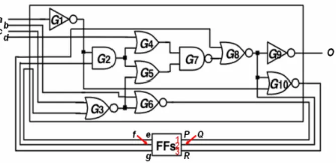
To motivate the use of clock skew scheduling for soft error tolerance, we use benchmark s27 (see Figure 1) from the ISCAS’89 suite, where flip-flops (FFs) are posi- tive-edge-triggered. Without loss of generality, we assume that the
delay of each gate is 1 (unit delay model) and wires do not contribute to the circuit delay. The assumption can be relaxed for a non-uniform delay model, with consideration of wire loads. In this example, we focus on a SEU which occurs at gate G8 and may be captured by flip-flops FF2 and/or FF3.
Definition 1 (error-latching window): The error-latching window [13] of a flip-flop is a time interval, [t–tsu, t+th], where t is the moment when a clock edge happens, tsu and th are the setup and hold times of the flip-flop. An error must be present during this interval to be latched; otherwise, it is filtered by latching-window (timing) masking. The error-latching window associated with a flip-flop can be backward propagated to internal gates (according to respective propagation delays) to determine when an error has to occur to be latched by that flip-flop.
Under unit delay model, the delays from G8 to FF2 and to FF3
are 0 and 1, respectively. Our goal is to overlap the error-latching windows of FF2 and FF3 at G8 by adjusting the arrival times of clock signals to FF2 and/or FF3, which in effect decreases the probability that an error at G8 is latched with increased impact of timing masking. The idea of overlapping error-latching windows, first proposed in [13], is based on the fact that the probability of timing masking is inversely proportional to the sum of sizes of disjointed error-latching windows. For example, in Figure 2(a), there are two separate error-latching windows at G8 (one at time t-1 and the other at t) before skewing any flip-flop. If we lengthen the arrival time of clock signals to FF3 by 1 and its new er- ror-latching window is shown as the upper right diagram in Figure 2(b), there will be only one joint error-latching window at G8 (at time t) due to complete overlapping. This implies that, after skewing FF3, only errors occurring at G8 during the error-latching window at time t will be latched, while errors occurring during the already-non-existing window at time t-1 will be filtered by timing masking, leading to a significant reduction in SER. Since the overlapped error-latching window (at time t) can be backward propagated to primary inputs, the positive impact on circuit SER is also valid for those gates in G8’s fanin cone.
However, in the case where FF3 has been skewed, MBUs may become more frequent because an error occurring at G8 during the joint error-latching window at time t will be latched by both FF2
and FF3 simultaneously. Instead of using all flip-flops in a sequential circuit as candidates for clock skew scheduling, we carefully pick pairs of flip-flops that are beneficial for MBU elimination. In the sequel, we demonstrate how to identify pairs of flip-flops that are capable of alleviating MBU effects (during clock cycles subsequent to particle hits) and suitable to be man- aged by CSS for MBU-aware soft error tolerance.
Figure 1. Example circuit s27
3.1. Implication-Based Masking
We consider the following example to illustrate the concept of implication-based masking required for our methodology. The function of primary output O of circuit s27 is:
O = (a + f’ + g)(c + d’ + e + g) (1) The complement of Boolean difference of O with respect to (w.r.t.) FF2’s present-state line f is:
F = (∂O/∂f)’ = a + c’de’ + g (2) Equation (2) represents the Boolean expression of logical masking patterns for errors propagated from f to O.
Similarly, the complement of Boolean difference of O w.r.t.
FF3’s present-state line g is:
G = (∂O/∂g)’ = (a + f’)(c + d’ + e) (3) Note that F is a function of g and G is a function of f, where f and g are present-state lines of FF2 and FF3 and may be corrupt due to the presumed SEU at G8. To remove f and g while keeping the logical masking patterns, we apply universal quantification.
The universal quantification of F w.r.t. g is:
e d c a F F
F g g
g = ⋅ = + ′ ′
∀ =1 =0 (4)
Equation (4) describes the patterns for logical masking of er- rors from f to O, for all possible values of g (0 and 1). Since we do not know whether g is corrupt, applying universal quantification makes sense and will correctly reflect logical masking of errors from f to O, irrespective of g.
Similarly, the universal quantification of G w.r.t. f is:
)
0 (
1 G a c d e
G
G f f
f = ⋅ = ⋅ + ′+
∀ = = (5)
Up to now, (4) and (5), which no longer include f or g, have been functions of inputs a, c, d, and e. In addition, one can find that (5) is a subset of (4); that is to say, with respect to O, the logical masking of an error on g implies the logical masking of an error on f. More precisely in this case, both errors on f and g will be masked when (5) is satisfied.
Definition 2 (implication-based masking): A pair of flip-flops X and Y is called an implication-based masking (IM) pair if, with respect to all outputs and flip-flops:
(i) the set of logical masking patterns for errors propagated from X (denoted by LM(X)) contains the one for errors from Y (de- noted by LM(Y)), i.e., LM(X) ⊇ LM(Y), or
(ii) the set of logical masking patterns for errors propagated from Y (LM(Y)) contains the one for errors from X (LM(X)), i.e., LM(Y) ⊇ LM(X).
Based on Definition 2, the first category of candidates for CSS can be identified. In circuit s27, as shown in Figure 1, (FF2 and FF3) is a pair of candidates falling into this category. By overlap- ping the error-latching windows of these two flip-flops via CSS (see Figure 2(b)), not only can SER be reduced, but also CSS-induced MBUs will be eliminated by implication with a certain probability. This will be demonstrated in Section 6.
3.2. Mutually-Exclusive Propagation
The second type of candidate flip-flops, mutually-exclusive propagation pair, in s27 can be identified by a single side-input
assignment, where a side input is a wire along which no error is propagated. Again, we focus on a SEU which occurs at G8 and may be captured by FF2 and/or FF3.
To propagate errors from FF3’s present-state line g to R, G10
needs a non-controlling value “0” on its side input G1ÆG10. As seen in Figure 1, the value assignment at the output of G1 is a controlling value for G2, at which errors from FF2’s present-state line f are thus logically masked. Therefore, with respect to R, the propagation of an error on g implies that an error propagated from f is logically masked. In other words, errors on f and g cannot be observable at R simultaneously.
Definition 3 (mutually-exclusive propagation): A pair of flip-flops X and Y is called a mutually-exclusive propagation (MEP) pair if, with respect to all outputs and flip-flops, the set of logical mask- ing patterns for errors propagated from X (LM(X)) contains the complement of the one for errors from Y (LM(Y)’), i.e., LM(X) ⊇ LM(Y)’. Intuitively, the sets of patterns for propagating errors from X and Y (LM(X)’ and LM(Y)’) are disjoint.
Based on Definition 3, the second category of candidates for CSS can be identified. Similar to IM pairs, we can overlap the error-latching windows of two flip-flops falling into this category (e.g., FF2 and FF3 in s27) to achieve MBU-aware soft error tolerance because, due to the property of mutually-exclusive propagation, at least one of the two errors propagated from this pair of flip-flops will be logically masked before reaching a primary output or a flip-flop. The mutually-exclusive property guarantees that the MBU impact after applying CSS is at most equivalent to the case of not applying CSS, whereas circuit SER can be significantly reduced as a result of increased timing masking. It is also probable that two errors from a MEP pair are both masked and consequently less MBU impact is expected.
Any two flip-flops are regarded as candidates and will be Figure 2. Overlapping of error-latching windows (a) Before skewing: two separate error-latching windows at G8
(b) After skewing: one joint error-latching window at G8
beneficial for SER reduction as long as they are either IM or MEP pairs. These two properties are the major motivation for our framework aiming at soft error tolerance, and both address the MBU issue by mitigating the occurrence of multiple-bit upsets.
More precisely, as mentioned earlier, overlapping the er- ror-latching windows of flip-flops increases the probability of timing masking and in turn decreases the soft error rate of a circuit.
Furthermore, overlapping the error-latching windows of a candi- date pair of flip-flops, which meet the IBM or MEP condition, can not only reduce circuit SER but also alleviate potential MBU effects. Hence, for our objective of MBU-aware soft error toler- ance, we check all possible pairs of flip-flops and extract as candidates for the proposed CSS-based framework those satisfy- ing the IM or MEP property.
4. Analysis of Soft Error Susceptibility
Before presenting the overall methodology for MBU-aware soft error tolerance, we briefly introduce two metrics associated with SER analysis in this section. The metrics, mean error impact (MEI) and mean error susceptibility (MES), are used to evaluate the circuit susceptibility to soft errors. Relying on a symbolic framework [14][15] which provides unified treatment of three masking mechanisms through decision diagrams, MEI and MES are calculated and thereafter, the soft error rate (SER) of a sequen- tial circuit can be derived accurately and efficiently.
4.1. Mean Error Impact (MEI) of Internal Gates
The MEI value of a gate quantifies the probability that at least one primary output is affected by an error originating at this gate.
The larger MEI a gate has, the higher the probability that an error occurring at this gate will be latched. This implies that those gates with higher MEI make the circuit more vulnerable to soft errors.
Please refer to [14][15] for more details about MEI.
4.2. Mean Error Susceptibility (MES) of Primary Outputs For each primary output Fj, initial duration d and initial am- plitude a, mean error susceptibility (MES) [14] is defined as the probability of output Fj failing due to errors at internal gates. In [14][15], the authors compute MES of each primary output in the circuit for a discrete set of pairs (d, a) of initial glitch durations and amplitudes. Then, the probability of output Fj failing (output failure probability) due to errors with various durations and amplitudes is calculated as a weighted sum of the discrete set of MES values. Finally, the soft error rate (SER) of output Fj can be derived based on the output failure probability.
5. Clock Skew Scheduling Based on Piecewise Linear Programming
The motivating example in Section 3 is a special case of CSS for MBU-aware soft error tolerance. A fundamental assumption in the example is that we can completely overlap the error-latching windows of a given pair of flip-flops (FFs) which have been recognized as candidates for CSS. This assumption is not realistic because it is not always possible to completely overlap er- ror-latching windows without incurring any timing violations, i.e., setup time violations owing to long paths or hold time violations owing to short paths. Moreover, adjusting the skew between two FFs may also change skews between affected FFs and unaffected FFs. For a large sequential circuit with hundreds of FFs, optimal skew scheduling, shown to be a signomial problem [16], is
difficult to be determined algorithmically. To address this problem, we develop an analytical method which can apply CSS with a global view on all extracted candidate FFs while suppressing timing violations. A generalized problem formulation, based on piecewise linear programming (PLP), is presented in the sequel.
5.1. Problem Formulation
Given a non-skewed sequential circuit (i.e., skew(FFi, FFj) = 0 for all i and j) and all possible pairs of flip-flops as candidates beneficial for MBU elimination, our objective is to achieve the highest level of MBU-aware soft error tolerance by maximizing the overlap between error-latching windows of each flip-flop pair via clock skew scheduling.
Definition 4 (intersecting gate): The intersecting gate of two flip-flops FFi and FFj is the root gate for the intersection of FFi’s and FFj’s fanin cones. In case of more than one such gate, the one with the largest MEI value is selected.
Definition 5 (skew): Given two flip-flops FFi and FFj for which the arrival times to clock pins are ci and cj respectively, the skew between FFi and FFj, denoted by skew(FFi, FFj), is (ci – cj).
In Figure 3, flip-flops FFi and FFj are a pair of candidates whose intersecting gate is gate Gij. The propagation delays from Gij to FFi and to FFj are denoted by di and dj respectively. Let the amounts of adjustments in the arrival times of clock signals to FFi
and FFj be si and sj, where si and sj can be positive or negative. To completely overlap the error-latching windows of FFi and FFj at Gij, we have to determine si and sj such that skew(FFi, FFj) = (si – sj) = (di – dj). But complete overlapping may need significantly large |si| and/or |sj| and thereby, may induce timing violations, which must be avoided in the resulting design. To suppress timing violations, we set up the first two constraints as follows.
For each possible pair of flip-flops FFx (skewed by sx) and FFy
(skewed by sy) between which there exist combinational paths from FFx to FFy, (6) is to prevent setup time violations and (7), hold time violations:
sx + tcq + Axy + tsu < sy + Tclk (6) sx + tcq + axy > sy + th (7) where Tclk is the clock period of the sequential circuit, tcq, tsu and th are respectively the clock-to-output delay, setup and hold times of flip-flops, and Axy and axy are the maximum and minimum delays Figure 3. Generalized clock skew scheduling of a candidate pair
of flip-flops (FFi and FFj) for MBU-aware soft error tolerance
of combinational paths from FFx to FFy, which can be obtained by performing static timing analysis.
Let wij denote the reduction in SER of the given circuit ob- tained by completely overlapping the error-latching windows of FFi and FFj at Gij. The reason for selecting an intersecting gate with the largest MEI is that, by doing so, it is very likely to obtain the largest wij for CSS.
The theoretical optimal SER reduction is:
∑
i,j(FFi,FFj)∈Candidates( ) wij (8)
Since the optimum (8) may be unachievable due to constraints (6) and (7), we use another variable, fij (0 ≦fij ≦wij), to denote the actual reduction in SER resulting from the overlapping (complete or partial) of FFi’s and FFj’s error-latching windows.
Figure 4 shows fij as a function of sij (= skew(FFi, FFj) = si – sj).
The rationale behind is that, once overlapped, fij is linearly proportional to the size of the overlap between FFi’s and FFj’s error-latching windows, and fij = wij when completely overlapped at sij = (di – dj).
From Figure 4, one can note that the relationship of fij versus sij is neither convex, nor concave. Instead, the formulation becomes piecewise linear if fij(sij) is broken into four pieces: sij = (di – dj) – (tsu + th), sij = (di – dj), and sij = (di – dj) + (tsu + th). By introducing four new binary variables pij,1, pij,2, pij,3, and pij,4 such that
pij,1 + pij,2 + pij,3 + pij,4 = 1 (9) and four new floating variables rij,1, rij,2, rij,3, and rij,4 where
0 ≦rij,k < pij,k for k = 1, 2, 3, and 4, (10) we can re-express sij as:
[ ]
[ ]
[ ]
[
(( ) () )( )]
) ( ) (
) (
) (
4 , 4
,
3 , 3
,
2 , 2
,
1 , 1
,
h su j i ij
h su j i ij
h su ij j i ij
h su ij h su j i ij
h su j i ij ij
j i ij
t t d d UB r t t d d p
t t r d d p
t t r t t d d p
LB t t d d r LB p
s s s
−
− +
−
× + + +
−
× +
+
× +
−
× +
+
× +
−
−
−
× +
−
−
−
−
× +
×
=
−
=
(11)
where LB and UB are the lower and upper bounds on sij. Similarly, fij can be rewritten as:
[ ]
[ ]
[ ]
[
0 0]
(0 )) 0 ( 0
0 0
4 , 4 ,
3 , 3 ,
2 , 2 ,
1 , 1 ,
× +
× +
−
× +
× +
−
× +
× +
× +
×
=
ij ij
ij ij
ij ij
ij ij ij
ij ij ij
r p
w r
w p
w r p
r p f
(12)
Geometrically, as shown in Figure 4, pij,k = 1 means sij is within the kth piece of fij(sij) and rij,k indicates the ratio of sij within the kth piece. For a valid solution, there must be only one among the four binary variables (pij,k) equal to 1 and only one among the four floating variables (rij,k) greater than or equal to 0. All of the other variables are 0.
Lastly, our proposed PLP-based SER mitigation framework, for MBU-aware soft error tolerance, is formulated as:
Maximize
∑
i,j(FFi,FFj)∈Candidates( ) fij (13)
Subject to (6), (7), (9), (10), and (11)
where (6) and (7) ensure no timing violation in the resulting circuit, and (9), (10), and (11) are used to transform the original formulation to a piecewise linear representation.
The optimal solution to (13) can be found by existing mixed integer linear programming (MILP) solvers. The worst-case problem size of our PLP formulation is O(n2) where n is the number of flip-flops in a circuit. This PLP-based methodology has been experimentally verified to be very efficient in runtime, of on the order of a minute for all benchmarks considered.
6. Experimental Results
In this section, we demonstrate various experiments of our proposed framework for MBU-aware soft error tolerance. The benchmark circuits are chosen from the ISCAS’89 suite. The technology used is 70nm, Predictive Technology Model (PTM).
The setup (tsu) and hold (th) times of flip-flops are both assumed to be 10ps. The overall methodology is implemented in C++, where the piecewise linear programming formulation is solved by GNU Linear Programming Kit (GLPK) version 4.33 on a 3GHz Pen- tium 4 workstation running Linux.
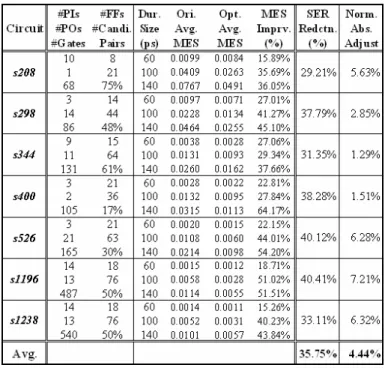
Table 1 reports the experimental results for average MES im- provement and SER reduction. For each benchmark in Table 1, we list the numbers of primary inputs, primary outputs and internal gates in column two, and the numbers of flip-flops, candidate pairs along with the corresponding percentage among all possible pairs in column three. For a circuit with n FFs, we check all possible (n*(n-1)/2) pairs and extract those satisfying the IM or MEP property as candidates for clock skew scheduling. The average MES values over all primary outputs before and after applying our PLP-based CSS are shown in columns five and six, for three different initial duration sizes (small: 60ps, medium:
100ps, and large: 140ps). Columns seven and eight demonstrate the MES improvement and the overall SER reduction. The runtime spent on solving the PLP problem, which is not included in the table, is about 1 minute for circuits s1196 and s1238 and very few or even less than 1 second for all the others.
For example, circuit s208 has 10 primary inputs, 1 primary output, 68 internal gates, and 8 flip-flops. Among 28 (= 8*7/2) pairs of FFs, 21 pairs (75%) can be identified as candidates for CSS. Based on (17), we formulate the CSS problem with these 21 pairs and then find its optimal solution by using GLPK. The MES improvements for small (60ps), medium (100ps), and large (140ps)
Figure 4. fij versus sij, with four pieces that are piecewise linear:
sij = (di – dj) – (tsu + th), sij = (di – dj), and sij = (di – dj) + (tsu + th)
duration sizes are 15.9%, 35.7%, and 36.1%, respectively. When considering all possible sizes of glitches, the overall SER reduc- tion is 29.2%. On average across all benchmarks, 35.8% SER reduction can be achieved.
Table 1 also shows the corresponding amount of skews due to CSS. This is measured by normalized absolute adjustment in clock signal, which is defined as:
clk i
i
T FF
⋅
∑
Δ FFs#
) (
AT (14)
where ΔAT(FFi) is the amount of adjustment in the arrival time of clock signal to FFi and Tclk is the clock period of the circuit.
Normalized absolute adjustment (14) quantifies the cost im- posed by CSS in terms of the degree of clock network modifica- tion. Intuitively, the larger the value of normalized absolute adjustment, the more aggressive modification the clock network may suffer. As it can be seen in the last column of Table 1, on average 4.4% normalized absolute adjustment is needed by our CSS-based framework. Note that the adjustment does not neces- sarily imply additional logic on the clock tree. For an H-tree structure, we can just unbalance wire loads during tree connec- tion/construction to implement the skews between pairs of FFs.
This is practically feasible, especially for those circuits which need significantly low adjustments in clock signals. For those circuits needing higher adjustments, wire sizing/rerouting and buffer sizing/relocation [17] are always the very first schemes for creating intentional skews.
Figure 5 shows the mitigation of MBU effects during clock cycles subsequent to particle hits (SEUs). In addition to the SER reduction for the first clock cycle via CSS, the potential CSS-induced MBU effects during the following cycles can be significantly mitigated by using IM and MEP pairs of flip-flops as candidates for CSS. On average across all subsequent cycles (from the 2nd to the 7th) in Figure 5, the MBU effects of circuits
s208 (see Figure 5(a)) and s298 (see Figure 5(b)) can be mitigated by 43% and 63%, respectively.
7. Conclusion
In this paper, we propose an analytical method for MBU-aware soft error tolerance of sequential circuits. The approach adjusts the arrival times of clock signals such that error-latching windows of flip-flops can be overlapped, which in effect increases the prob- ability of timing masking and decreases the soft error rate of a sequential circuit. Moreover, two types of candidate pairs of flip-flops, beneficial for MBU elimination, are introduced. The overall methodology using clock skew scheduling is formulated as a piecewise linear programming problem and can be solved efficiently by GLPK. Experiments on a set of ISCAS’89 bench- marks reveal the effectiveness of our framework.
References
[1] R. Baumann, “Soft errors in advanced computer systems,” IEEE Design and Test of Computers, May 2005.
[2] Y. S. Dhillon et al., “Analysis and optimization of nanometer CMOS circuits for soft-error tolerance,” IEEE Trans. on VLSI, May 2006.
[3] S. Mitra et al., “Robust system design with built-in soft-error resilience,”
IEEE Computer Magazine, Feb. 2005.
[4] P. Shivakumar et al., “Modeling the effect of technology trends on the soft error rate of combinational logic,” in Proc. of Int’l Conf. on De- pendable Systems and Networks, June 2002.
[5] Q. Zhou and K. Mohanram, “Gate sizing to radiation harden combina- tional logic,” IEEE Trans. on CAD, Jan. 2006.
[6] S. Almukhaizim et al., “Seamless integration of SER in rewiring-based design space exploration,” in Proc. of ITC, Oct. 2006.
[7] K. Mohanram and N. A. Touba, “Cost-effective approach for reducing soft error failure rate in logic circuits,” in Proc. of ITC, Sep. 2003.
[8] M. R. Choudhury, Q. Zhou, and K. Mohanram, “Design optimization for single-event upset robustness using simultaneous dual-VDD and sizing technique,” in Proc. of ICCAD, Nov. 2006.
[9] K.-C. Wu and D. Marculescu, “Power-aware soft error hardening via selective voltage scaling,” in Proc. of ICCD, Oct. 2008.
[10] S. Krishnaswamy et al., “Enhancing design robustness with reliabil- ity-aware resynthesis and logic simulation,” Proc. of ICCAD, Nov. 2007.
[11] M. Zhang et al., “Sequential element design with built-in soft error resilience,” IEEE Trans. on VLSI, Dec. 2006.
[12] V. Joshi et al., “Logic SER reduction through flipflop redesign,” in Proc.
of ISQED, March 2006.
[13] S. Krishnaswamy, I. L. Markov, and J. P. Hayes, “On the role of timing masking in reliable logic circuit design,” in Proc. of DAC, June 2008.
[14] N. Miskov-Zivanov and D. Marculescu, “Soft error rate analysis for sequential circuits,” in Proc. of DATE, April 2007.
[15] N. Miskov-Zivanov and D. Marculescu, “A systematic approach to modeling and analysis of transient faults in logic circuits,” in Proc. of ISQED, March 2009.
[16] J. P. Fishburn, “Clock skew optimization,” IEEE Trans. on Computers, July 1990.
[17] J. L. Neves and E. G. Friedman, “Design methodology for synthesizing clock distribution networks exploiting nonzero localized clock skew,”
IEEE Trans. on VLSI, June 1996.
Table 1. Average mean error susceptibility (MES) improvement and overall soft error rate (SER) reduction
Figure 5. Mitigation of MBU effects during clock cycles subse- quent to particle hits (SEUs)
(a) s208 (b) s298