A New FPGA Implementation Of Four- Switch Three- Phase Inverter
Phan Quoc Dzung
Faculty of Electrical &
Electronic Engineering HCMC University of
Technology Ho Chi Minh City,
Vietnam [email protected]
Le Minh Phuong
Faculty of Electrical &
Electronic Engineering HCMC University of
Technology Ho Chi Minh City,
Vietnam [email protected]
Hong Hee Lee
NARC, Ulsan University, Korea [email protected]
Bui Ngoc Thang
HCMC University of Technology Ho Chi Minh City,
Vietnam buingocthang1984@yahoo.
com
Le Dinh Khoa
Faculty of Electrical &
Electronic Engineering HCMC University of
Technology Ho Chi Minh City,
Vietnam
[email protected]
Abstract -- This paper is concerned on FPGA design for control implementations of four switch three phase inverters (B4, FSTPI). This paper is to present a space vector PWM algorithm for four switch three phase inverters (B4, FSTPI) based on the one for six switch three phase inverters (B6, SSTPI) (principle of similarity) where the αβ plan is divided into 6 sectors and the formation of the required reference voltage space vector is done in the same way as for B6 by using effective (mean) vectors. An SVPWM technique has been developed using the ready-to-use field-programmable gate array (FPGA) technology. High speed, very large number of components, large number of supported protocols, and addition of ready-to-use intellectual property cores make programmable devices the preferred choice of implementation and even deployment mass production quantities of Power Electronics. Matlab/Simulink is used for the simulation of the proposed SVPWM algorithm. A Field Programmable Gate Array (FPGA) From Xilinx Inc - Spartan 3E was used at the main of the control electronics. The simulation and experimental results are demonstrated.
Index Terms - Field-programmable gate array (FPGA), four switch three phase inverters (B4, FSTPI), six switch three phase inverters (B6, SSTPI), space vector PWM, VHDL.
I. I NTRODUCTION
Three phase variable speed drives for asynchronous motors have been used more and more, especially in energy saving drive applications for fans, pumps, air compressors… In many cases, the cost reduction is an important target for the drive.
To reduce number of power semiconductor devices in a three phase voltage inverter, where there are only 4 switches, were proposed different control methods. One of them is [1], which presents a new space vector PWM algorithm for four switch three phase inverters (B4, FSTPI) based on the one for six switch three phase inverters.
The rapid development in high-performance low-cost digital signal processors (DSP’s) [2], [3] has encouraged research on digital PWM control [4], [5] and digital current control [6] - typical control architecture of a DSP-based ac drive is presented. However, generating PWM gating signals and current control loops requires a high sampling rate to achieve a wide bandwidth performance. Therefore most computation resources of the DSP must be devoted to generating the PWM signals and executing of current control
algorithms [7]. As a result, only limited functions are left for other control loops and functions and complicate the design process enormously [8].
Recently, the FPGA devices have been improved and their application has expanded from prototyping tasks to telecommunication, image and sound processing and many others. The properties of the algorithm processing, such as capability of performing real parallel calculations combined with solutions’ flexibility, are probably the main reasons for applying the FPGA to many technical domains. Many available matrices contain, specialized digital signal processing blocks capable of performing hardware multiplication with accumulation, and block providing with the advanced input-output configuration with digitally controlled impedance feature. The possibility of developing a real hardware implementation of the signal processing algorithms is also a great merit [9][10]
The paper presents the application of FPGA (Spartan 3E from Xilinx, Inс) to realize the SVPWM technique for B4 inverter (FSTP) modeled on the basis of a B6 by using the principle of similarity and revealing perspective solution for the PWM in the zone of overmodulation when the PWM is quite complicated due to the nonlinear character of modulation in this extended zone. The principal control schema is presented in Fig.1.
Fig.1. Four switch three phase inverter (FSTPI) is based on FPGA II. A NALYSIS O F S PACE V OLTAGE V ECTORS
According to the scheme in Fig.2 the switching status is
PEDS2009
represented by binary variables S1 to S4, which are set to “1”
when the switch is closed and “0” when open.
4
1
1
+S =
S ; S
3+S
2= 1 (1) Phase to common point voltage depends on the turning off signal for the switch:
( 2
11 ) 2 ;
0( 2
31 ) 2 ;
00 ;
0
= − ⋅ = − ⋅
c=
dc b
dc
a
V V
S V V
S
V (2)
Combinations of switching S1-S4 result in 4 general space vectors V G
1V G
4→ (Table 1).
Fig.2. Sectors used in conventional SVPWM methods for B4 TABLE I
C
OMBINATIONS OFS
WITCHINGS ANDV
OLTAGES
PACEV
ECTORSIII. M ODIFIED S VPWM A PPROACH F OR B4 I NVERTER SVPWM methods presented in papers [11, 12, 13, 14, 15]
are based on the formation of the reference vector on the plan αβ which is divided into four sectors (sector I...IV). The active vectors and their duration in one sampling interval are selected and calculated on the basis of the required Vref location respective for these sectors (fig.3).
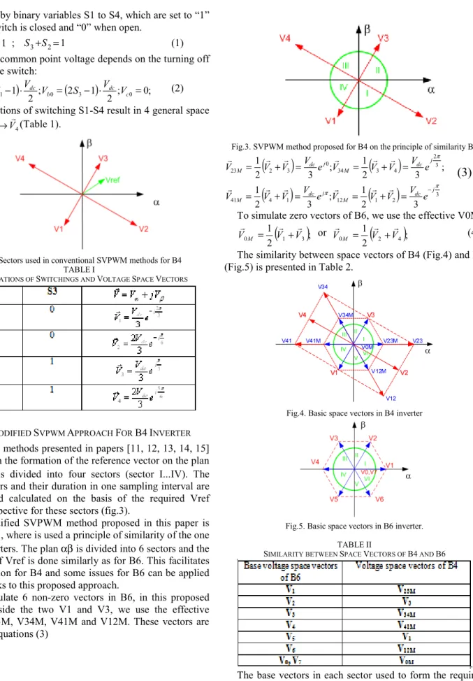
The modified SVPWM method proposed in this paper is based on [1], where is used a principle of similarity of the one for B6 inverters. The plan αβ is divided into 6 sectors and the formation of Vref is done similarly as for B6. This facilitates the calculation for B4 and some issues for B6 can be applied for B4 thanks to this proposed approach.
To simulate 6 non-zero vectors in B6, in this proposed method, beside the two V1 and V3, we use the effective vectors V23M, V34M, V41M and V12M. These vectors are formed as equations (3)
Fig.3. SVPWM method proposed for B4 on the principle of similarity B6
( ) ( )
(
4 1)
12(
1 2)
341
3 2 4
3 34
0 3
2 23
3 2
; 1 3 2
1
3 ; 2
; 1 3 2
1
π π
π
dc j M
dc j M
dc j M
dc j M
V e V V V
V e V V V
V e V V V
V e V V V
=
−+
=
= +
=
= +
=
= +
=
G G G
G G G
G G G
G G G
(3)
To simulate zero vectors of B6, we use the effective V0M:
( ) ;
2 1
3 1
0
V V
V G
MG G
+
= or V G
0M= 2 1 ( V G
2+ V G
4) ; (4) The similarity between space vectors of B4 (Fig.4) and B6 (Fig.5) is presented in Table 2.
Fig.4. Basic space vectors in B4 inverter
Fig.5. Basic space vectors in B6 inverter.
TABLE II
S
IMILARITY BETWEENS
PACEV
ECTORS OFB4
ANDB6
The base vectors in each sector used to form the required
PEDS2009
space vector Vref is presented in Table 3.
T ABLE III .
V ECTORS USED IN THE S PACE V ECTOR M ODULATION B6 & B4
Fig.6 and Fig.7 presents pulse patterns for switching in the proposed method for six sectors.
Fig.6. Pulse patterns for switching in the proposed method (For sectors I, V, VI)
Fig.7. Pulse patterns for switching in the proposed method (Sectors II, III, IV)
Below we will describe the space vector modulation for B4 inverter based on the modulation for B6 with the principle of similarity: The required voltage space vector rotates in a hexagon and the space vector modulation is based on the formation of three voltage vectors in sequence in one sampling interval Ts so that the average output voltage meets the requirement. The calculations of the switching states in B6 and B4 are as follows for ½ Ts [10]:
( )
( )
y x s z
s y
s x
t t T t
MT t
MT t
−
−
=
=
−
=
2 /
; 3 sin
; 3 / 3 sin
π α
α π π
(5)
Where:
tx - duration for vector Vx ty - duration for vector Vy tz - duration for vector Vz
M – The index of modulation M = V*/V1sw (V* - amplitude of the required voltage vector, V1sw – peak value of six step voltage).
However in B4 inverter since mean vectors tXYM and zero vectors t0M are formed from the two base vectors the duration of base vectors is equal to ½ as for the above
mentioned mean and zero vectors.
It can be used, for example, the effective vectors V23M, V3, V0M for sector I, where V23M, V0M are defined as (11):
( ) ( )
; 2
; 2
; 2 2
; 2
/
; 3 sin
; 3 / 3 sin
0 1 0 3 23 3 23 2
3 23
3 23
f z f z f m f m
f f s of z
s f
y s
f x
t t t t
t t t t
t t T t t
MT t
t MT
t t
=
=
=
=
−
−
=
=
=
=
−
=
= α
α π π π
(6)
Thus the total durations for base vectors V1, V2, V3 are:
z m f V
m V
z V
t t t t
t t
t t
3 3 3 3
2 2
1 1
;
;
+ +
=
=
= (7)
Similarly we can calculate the space vector modulation for the other sectors. The calculation results are shown in Table IV.
T ABLE IV .
V ECTOR D URATIONS IN THE P ROPOSED S VPWM M ETHOD
Sector I Sector II
( )
( )
; 2 2
2 ; 2 ;
; 2
/
; 3 sin
; 3 / 3 sin
0 1 0 3
23 3 23 2
3 23 3
23
f z f z
f m f m
f f s of z
s f
y
s f
x
t t t t
t t t t
t t T t t
MT t
t
MT t
t
=
=
=
=
−
−
=
=
=
=
−
=
= π α
α
π π ( )
( )
; 2 2
2 ; 2 ;
; 2
/
; 3 sin
; 3 / 3 sin
0 1 0 3
34 4 34 3
34 3 34
3
f z f z
f m f m
f f s of z
s f
y
s f
x
t t t t
t t t t
t t T t t
MT t
t
MT t
t
=
=
=
=
−
−
=
=
=
=
−
=
= π α
α π π
z m f V
m V
z V
t t t t
t t
t t
3 3 3 3
2 2
1 1
+ +
=
=
=
z m f V
m V
z V
t t t t
t t
t t
3 3 3 3
4 4
1 1
+ +
=
=
=
Sector III Sector IV
( )
( )
; 2 2
2 ;
2 ;
; 2 2
; 2
/
; 3 sin
; 3 / 3 sin
0 1 0 3
41 1
41 34 4 34 3
41 34 41
34
f z f z
f m
f f m f m
f f s of z
s f
y
s f
x
t t t t t t
t t t
t t
t t T t t
MT t
t
MT t
t
=
=
=
+
=
=
−
−
=
=
=
=
−
=
= π α
α
π π ( )
( )
; 2 2
2 ; 2 ;
; 2
/
; 3 sin
; 3 / 3 sin
0 1 0 3
41 1 41 4
1 41 1
41
f z f z
f m f m
f f s of z
s f
y
s f
x
t t t t
t t t t
t t T t t
MT t
t
MT t
t
=
=
=
=
−
−
=
=
=
=
−
=
= π α
α π π
z m V
m V
z m V
t t t
t t
t t t
3 3 3
4 4
1 1 1
+
=
= +
=
z V
m V
z m f V
t t
t t
t t t t
3 3
4 4
1 1 1 1
=
=
+ +
=
Sector V Sector VI
PEDS2009
( ) ( )
; 2 2
2 ; 2 ;
; 2
/
; 3 sin
; 3 / 3 sin
0 1 0 3
12 2 12 1
12 1 12
1
f z f z
f m f m
f f s of z
s f
y
s f
x
t t t t
t t t t
t t T t t
MT t
t
MT t
t
=
=
=
=
−
−
=
=
=
=
−
=
= π α
α
π π ( )
( )
; 2 2
2
2 ;
; 2 2
; 2
/
; 3 sin
; 3 / 3 sin
0 1 0 3
23 3
23 12 2 12 1
23 12 23
12
f z f z
f m
f f m f m
f f s of z
s f
y
s f
x
t t t t t t
t t t
t t
t t T t t
MT t
t
MT t
t
=
=
=
+
=
=
−
−
=
=
=
=
−
=
= π α
α π π
z V
m V
z m f V
t t
t t
t t t t
3 3
2 2
1 1 1 1
=
=
+ +
=
z m V
m V
z m V
t t t
t t
t t t
3 3 3
2 2
1 1 1