國
立
交
通
大
學
電子工程學系 電子研究所
博 士 論 文
第二型砷化銦鎵/砷銻化鎵 “W”量子井之光學特性及
光激發中紅外線雷射之研究
Optical Characteristics of Type-II InGaAs/GaAsSb “W”
Quantum Wells and Optically-Pumped Mid Infrared Lasers
研 究 生:潘建宏
指導教授:李建平 教授
第二型砷化銦鎵/砷銻化鎵 “W”量子井之光學特性
及光激發中紅外線雷射之研究
Optical Characteristics of Type-II InGaAs/GaAsSb “W”
Quantum Wells and Optically-Pumped Mid Infrared Lasers
研 究 生:潘建宏 Student:Chien-Hung Pan
指導教授:李建平 Advisor:Dr. Chien-Ping Lee
國 立 交 通 大 學
電子工程學系 電子研究所
博 士 論 文
A Dissertation
Submitted to Department of Electronics Engineering and Institute of Electronics
College of Electrical and Computer Engineering National Chiao Tung University
in Partial Fulfillment of the Requirements for the Degree of
Doctor of Philosophy in
Electronics Engineering
November 2012
Hsinchu, Taiwan, Republic of China
i
第二型砷化銦鎵/砷銻化鎵 “W” 量子井之光學特性及
光激發中紅外線雷射之研究
研究生:潘建宏 指導教授:李建平 博士 國 立 交 通 大 學 電子工程學系電子研究所 博士班 摘要 此篇論文主要貢獻在探索與開發半導體中紅外線光源,有別於一般較昂貴且不成熟的銻 化鎵及砷化銦基材,我們使用較普遍且散熱較佳的磷化銦基板成長第二型砷化銦鎵/砷銻化 鎵 “W”量子井。不同於一般第二型電洞的量子井,此“W”結構藉由阻擋層(barrier layer)對電子侷限來增加電子電洞波函數耦合並提升光躍遷率。 我們透過理論計算改變各結構參數(例如量子井厚度及砷銻化鎵的比例成分)能得到 2 到 3 微米的發光範圍並且得知發光波長的延伸與光耀遷率的強度有一交替關係(trade-off), 亦即發光波長越長通常伴隨光躍遷率的下降,此為“W”結構本質的特性。而在給定一個發 光波長下,較薄量子井厚度及較高銻成分的結構設計組合能提供較高的電子電洞耦合。我 們更進一步用八個能帶的k.p理論來計算能帶關係及不同載子濃度下的材料光增益,在 適當的設計下單一層量子井增益即能達到 103 cm-1 ,此已符合一般雷射元件的需求。我們也 顯示出藉由適當增加電洞量子井的壓縮應變,能使電子電洞的等效質量較平衡進而降低透 明載子濃度(transparency carrier density)及提高材料光增益。ii 別改變砷化銦鎵、砷銻化鎵的厚度以及砷銻化鎵合金中銻的比例,在低溫下樣品的光激發 螢光光譜可顯示出 2-2.5 微米的波長範圍,其螢光強度與發光波長如前所述有一交換關係, 並且如理論預測其螢光積分強度與計算的電子電洞波函數耦合平方成正比。樣品品質表現 良好,螢光積分強度從低溫到室溫只約下降了 10 倍。在室溫下我們首次展示出其波長能超 過 3 微米。我們透過變功率光激發螢光實驗來研究“W”量子井中第二型能帶排列的特徵, 光譜的峰值位置隨激發功率增加而藍移,但不同於一般第二型量子井其藍移量並未與激發 光功率的 1/3 次方成正比,對此現象我們提出局域的能態填充(localized states band filling)來解釋,其局域能態來自於合金成分的不均勻及磊晶層表面起伏所致,模擬結果 與實驗值可以得到良好的吻合。 最後我們首次成功的展示室溫操作光激發 2.56 微米的“W”量子井中紅外線雷射,此 為所知在磷化銦基板上波長最長的能帶間躍遷(interband transition)雷射,其閥值功 率密度約為 40kW/cm2 ,其特徵溫度 T0在操作溫度小於 250K 時為 487.8K,而從 250K 到室溫 其 T0為 41.8K,此劇烈的 T0變化及較小的室溫 T0我們認為是歐傑複合所導致,經由不同雷 射腔長的實驗萃取波導光損耗以及理論計算波導模態增益,我們得以估計歐傑常數約為 1.67 x10⁻²⁷ cm6 /s。 最後我們提出並評估一方法能將“W”量子井發光波長延升至 3-5 微米波段,此即成長緩 衝層將晶格常數轉至~5.94Ao ,並接著使用 In0.7Ga0.3As/GaSb/In0.7Al0.3As “W” 量子井的結構 設計。
iii
Optical Characteristics of Type-II InGaAs/GaAsSb “W” Quantum
Wells and Optically-Pumped Mid Infrared Lasers
Student: Chien-Hung Pan Advisor: Dr. Chien-Ping Lee Department of Electronics & Institute of Electronics
National Chiao Tung University
Abstract
This dissertation mainly dedicates to explore and develop mid-infrared light sources. In difference with usual expensive and immature InAs-based and GaSb-based materials, we utilized more popular, better thermal conductive InP substrates and employed type-II InGaAs/GaAsSb “W” type quantum wells (QWs). Distinguishing from general type-II hole quantum well, the “W” structure includes barrier layers to confine electrons and to increase electron-hole wavefunction overlap, hence the optical transition rate.
Through theoretical calculations changed with structure parameters (such as QWs thickness and GaAsSb composition), a range of 2-3m emission wavelength can be derived. It also shows a trade-off situation between the extending of emission wavelength and the intensity of optical transition rate, meaning a longer emission wavelength generally accompanied with a decreased optical transition rate, which is an intrinsic feature for the “W” structure. However, at a given emission wavelength, the design with thinner InGaAs and GaAsSb layers and a higher Sb content in GaAsSb is more desirable, which could provide of a larger electron-hole wavefunction overlap. We further used the eight-band k.p theory to calculate the E-k relation and material gain as a function of carrier density. With a proper design, the material gain of a single “W” QW is able to reach above 103 cm-1, which is sufficient for general mid-IR lasers applications. We also pointed out that adopting proper compressive strain in hole QW makes a more balanced electron and hole
iv
masses that could reduce the transparency carrier density and increase the material gain.
In experiments, we grew a series of samples systematically varied with thickness of InGaAs, thickness of GaAsSb and Sb mole fraction in GaAsSb. The photoluminescence (PL) spectra of samples cover the range of 2-2.5 m at low temperature. The trade-off between optical transition rate and wavelength emission is confirmed as the prediction of the theoretical calculations, where the integrated PL intensity is proportional to the square of electron-hole wavefunction overlap. The samples showed good optical quality that integrated PL intensity only decreases an order from cryogenic temperature to room temperature (RT). For the first time we demonstrated PL emission wavelength longer than 3 m at RT by the InP-based “W” structure. The type-II band alignment in the “W” structure has been characterized by the power dependent PL measurements. The peak position shifts to shorter wavelength as the excitation power (Pex) increases. It was
found the amount of energy shifts does not follow the Pex1/3 law as most type II structures. The
localized states filling effect due to the surface roughness and alloy fluctuation is proposed to explain the observed phenomenon. The calculated results agree well with the experiment results.
For the first time we demonstrated the room temperature optically-pumped mid-IR “W” type lasers on InP substrates. The lasing wave length is 2.56 µm, which is known as the longest for the InP-based interband transition, with a threshold pumping power density of ~40kW/cm2. The laser shows a characteristic temperature (T0) of 487.8K as operated below 250K and a T0 of 41.8K as
operated near room temperature. This abrupt T0 change and the small T0 at room temperature are
considered due to the dominated Auger processes. An Auger coefficient of 1.67x10⁻²⁷ cm6/s was estimated via different laser cavity length studies for the extraction of waveguide optical loss and theoretical calculations for the waveguide modal gain.
v
wavelengths into 3-5m regime, which uses a metamorphic buffer layer to shift the lattice constant to ~5.94Å and then grows the designed “W” QW structure of In0.7Ga0.3As/
vi
致謝
第一個要感謝的就是李建平老師,是以無私的付出與廣闊的胸襟,能成就如此規模的實 驗室,讓我能在裡頭馳騁、犯錯以及學習,老師總在適時給予提點,在論文上給予關鍵的 指導,能遇到如此好的老師,總深深地感到幸運及感恩。接著感謝林聖迪老師幫忙維護整 個大實驗室的運作,當然包括辛勞的MBE事務,從老師身上也看到對道理追求的態度。 感謝林國瑞老師,光電子學課程真的很受用。感謝曾經一起生活的畢業學長們:羅明城博 士、凌鴻緒博士及林大鈞博士,有你們的傳承及實驗的討論使研究順利不少。感謝實驗室 一同奮鬥的夥伴們:鄭旭傑、蘇聖凱、林建宏、林岳民、傅英哲、張家豪、林仕偉、李宗 霖、徐偉程、周柏存…等,在實驗上互相幫忙及討論,還能一起熱血的運動流汗,讓彼此 都很健康,可以分享喜怒哀樂,掃除研究路途上的陰霾。最後,最重要的,要感謝我最親 愛的家人,我的父母及姊姊,沒有爸媽你們建立如此健全沒有經濟負擔的家庭,還有對我 人生路上的指引,便沒有今日的我,能當你們兒子真有福氣,真要好好感謝你們,榮耀你 們。vii
CONTENTS
Abstract (Chinese) ………i
Abstract (English) ………...iii
Acknowledgement ………..vi
Contents ………...vii
Table captions ………... x
Figure captions………...xi
Chapter 1: Introduction………...…1
1.1 Mid infrared applications………...…1
1.2 A brief review of III-V semiconductor mid-IR lasers………...….3
1.3 Research motivation………...……8
1.4 Organization of this dissertation………...9
Chapter 2: Theoretical studies of InGaAs/GaAsSb type-II “W” type quantum
wells on InP substrates………...11
2.1 Band alignments of “W” type quantum well………...………11
2.2 The trade-off feature for the “W” type quantum well explored by one
band effective mass approximation………...20
2.3 Energy band dispersion relations and material gain simulations of “W”
viii
quantum wells based on the eight band k.p theory………..25
2.4 Summary………...…...39
Chapter 3: Experiment techniques………...……40
3.1 Molecular beam epitaxy………...…40
3.1-1 Chambers’ configurations, utilities and functions…………...42
3.1-2 Calibrations of growth rate and doping concentration………...44
3.1-3 Sample growth procedure………...45
3.2 Material characteristics analysis………...47
3.2-1 High resolution X-ray diffraction system………...47
3.2-2 Photoluminescence Spectroscopy………...48
3.2-3 The setup for optically-pumped lasers measurement………….49
Chapter 4: 2~3
m mid infrared light sources using InGaAs/GaAsSb “W”
type quantum wells on InP substrates………..52
4.1 The growth of ternary alloys lattice-matched to InP substrate ……...52
4.2 The growth condition dependence of Sb fraction in GaAsSb alloy....54
4.3 “W” type quantum well sample growth………...…56
4.4 Photoluminescence results and discussion………...……58
ix
Chapter 5: Room temperature optically-pumped mid-IR lasers with “W” type
InGaAs/GaAsSb quantum wells on InP substrates……….67
5.1 The structure of type-II “W” QWs mid-IR laser…...67
5.2 E-k band structure calculation and waveguide simulation………...…68
5.3 Experimental results and laser characteristics discussion………....…70
5.4 Conclusions………...77
Chapter 6: Conclusions and Future works………...78
6.1 Conclusions of present studies………...78
6.2 Suggestions for future works………...80
6.2-1 Extending the InP-based “W” QWs into 3-5
m regime……….80
6.2-2 Dual wavelength lasing of optically-pumped mid-IR lasers
and fabrication of tunable optically-pumped DFB laser...82
6.2-3 Fabrication of electrical injection InP-based “W” mid-IR lasers.89
Reference………...90
Vita………...96
x
Table Captions
Table 2.1 Room temperature (300K) and low temperature (0K) direct band gaps of ternary alloys lattice matched to InP substrate………..12 Table 2.2(a) Band structure parameters for binary semiconductors of InAs, GaAs, and GaSb………..16 Table 2.2(b) Bowing parameters for InGaAs and GaAsSb………...17 Table 2.3 The conduction and valence bad effective mass values of ternaries used for simulations………21 Table 2.4 The equations used to calculate parameter values of ternary alloys in the “W” structure……….32 Table 2.5 The temperature dependences of band gaps and lattice constants for the three alloys……….33 Table 2.6 The Ec/Ev band offsets of GaAsSb/InGaAs type-II heterostructure and the
extracted values of effective band gap, the energy differences of C1-C2 and HH1-LH1, and the C1 electron /HH1 hole effective masses at zone center for the three cases……….……..33 Table 4.1 The InGaAs/GaAsSb layer thickness, the Sb2/As2 BEPratio, the summarized PL
xi
Figure Captions
Fig.1.1 (a) A Scheme of a typical setup for mid-IR spectroscopy. (b) Absorption lines and intensity of some important molecules (derived from Hitran database [ref. 3])……….2 Fig 1.2(a) Direct -valley band gaps of binary (filled dot) and ternary (joined curve) III-V semiconductors. (b) Relative band alignments of conduction band (CB) and valence band (VB) edges for binary semiconductors [ref. 1]. ………..3 Fig 1.3(a) Band alignments and fundamental electron-hole optical transition of type-I, and (b) type-II QW lasers [ref. 7]. ………..6 Fig 1.3(c) Band alignment along with ground state electron and hole wavefunctions of type-II “W” structure QWs. (d) Band profile (not to scale) under bias of an interband quantum cascade active region and also indicated with the carrier optical transition in the AlSb/InAs/GaSb quantum well [ref. 8]………...7 Fig 2.1 Band lineups, with values of conduction and valence band offsets (ΔEc and ΔEv)
indicated, of the four ternary alloys lattice matched to InP substrate………...…12 Fig 2.2 Strain effects induced band edge shifts for the three cases: tensile-strained, unstrained, and compressive-strained………..………15 Fig. 2.3(a) Energy shifts of band edges, including conduction (Ec), heavy hole (Ehh), and light
hole (Elh) bands, vs. indium fraction for InGaAs pseudomorphic layer, and Fig. 2.3(b) those
for GaAsSb pseudomorphic layer with varied antimony fraction on InP substrate…………..17 Fig. 2.4 A Scheme of a typical band alignment for the “W” type QW along with fundamental electron and hole wavefunctions………..……….18 Fig. 2.5 Band edge energy levels (conduction band edge Ec denoted by solid line and valence
band edge Ev by dashed line) of In0.53Ga0.47As and In0.52Al0.48As which are lattice matched to
InP substrate, and GaAs1-xSbx pseudomorphic layer with Sb fraction varied from 0 to1. The
biaxial strain is indicated on the top horizon axis. The band gap values for each material are indicated by the arrows. The Δ denotes the energy separation between the Ec of In0.53Ga0.47As
and the Ev of In0.53Ga0.47As………...……….19
Fig. 2.6(a) 3D contour plots and (b) corresponding wavefunction overlap square displayed in correlated grayscale at three wavelengths based on calculations using the one-band effective mass approximation………..…23 Fig. 2.7(a) The band diagram and calculation results of wavefunctions for a chosen “W”
xii
structure, indicated with values of structure parameters, emission wavelength, and electron-hole wavefunction overlap. For comparison, (b), (c), and (d) are results with increased thickness of InGaAs, GaAsSb, and Sb fraction of GaAsSb respectively. By comparing to (a), each shows a trade-off behavior, Extending wavelength accompanying with the reduction of wavefunction overlap………..24 Fig. 2.8 The energy dispersion of the “W” QW consisting of In0.53Ga0.47As
/GaAs1-xSbx/In0.53Ga0.47As (4/3/4nm) sandwiched between In0.52Al0.48As barrier layers for the
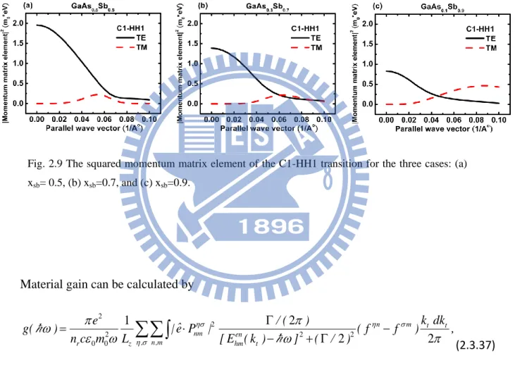
three cases with different Sb fraction: (a) xsb= 0.5, (b) xsb=0.7, and (c) xsb=0.9, where C1 and
C2 refer to the symmetric and the anti-symmetric conduction subbands, HH1 and HH2 refer to the first and the second confined heavy hole subbands, and LH1 refers to the first confined light hole subband……….………34 Fig. 2.9 The squared momentum matrix element of the C1-HH1 transition for the three cases: (a) xsb= 0.5, (b) xsb=0.7, and (c) xsb=0.9………..…..36
Fig. 2.10 The calculated TE material gain spectra for the three cases with 2D carrier densities of 1x10¹², 2x10¹², and 3x1012 cm-2………..…….37 Fig. 2.11 The TE material gain peak value as function of carrier 2D density for the three cases………..38 Fig. 3.1 Front view of the Lm MBE and Rn MBE linked with a center extension chamber....41 Fig. 3.2(a) side view and (b) rear view of the Rn MBE………....41 Fig. 3.3 The configuration sketch of the Rn MBE. Three parts of the system, Entry/exit, buffer, and growth chambers, are divided and separated by gate valves. The Entry/exit chamber functioned for sample loading is equipped with a cryo pump for ultra-high vacuum (UHV) maintenance and a heater for the 200oC bake. The buffer chamber functioned for wafer preparation is equipped with a heated station for wafer baking and an ion pump for UHV maintenance. The growth chamber functioned for wafer epitaxy is equipped with shutter controlled effusion cells contained sources of As, Sb, Al, Ga, In, and with dopant cells of Si, Be, and Te. The CAR holds the wafer during growth process, which could control the growth temperature and rotate continuously for the deposition uniformity. The RHEED system uses high energy electron beams hitting the wafer surface to in-situ monitor growth condition. The pyro meter monitors wafer surface temperature via optical detection. The growth chamber is equipped with a residue gas analyzer to analyze kinds of molecules inside the chamber and to
xiii
detect leakage. The UHV environment is maintained by an ion pump and a cryo pump, and assisted by the liquid nitrogen flow in cry-panel during growth.……….……42 Fig. 3.4 REED intensity oscillation trace for the case of InAs growth.………45 Fig. 3.5 Gallium BEP linearly depends with growth rate for the case of growing GaAs.……45 Fig. 3.6 Etched C-V measurement for doping check of the Be case, which is the result of 5 layers of GaAs, each 700nm thick, doped with various Be concentrations using different cell temperatures.………..45 Fig. 3.7 The relationship of doping concentration and doping temperature of the Be cell..….45 Fig. 3.8 The streaky RHEED pattern randomly taken during desorption process on (001) GaAs substrate. The pattern evolves periodically as the substrate rotates and the substrate direction paralleled to electron beam varies between [100] and [010] directions.………...…46 Fig. 3.9 X-ray data scanned in mode for the example of three GaAsSb layers grown on an InP substrate, where peak position values are noted………..…………..47 Fig. 3.10 The Scheme of the PL setup of our lab. The excitation source form an Ar+ laser beam (488nm/ 514nm) is directed via mirror reflections, going through chopper, density filter, and focused on to sample surface via a CaF2 lens. The sample is placed on a copper chuck
mounted on a closed cycle cryogenic system capable of temperature tuning from ~10K to 390K. The spontaneous emission is collected by two CaF2 lenses, passing through a laser
filter, and arrives at the entrance slit of the IHR550 monochromator. The singles from the photo detector, which is in the exit slit of the monochromator, finally go to the computer after processing with a conventional lock-in technique….………..………..………49 Fig. 3.11 The 1064 nm fiber laser output peak power as function of output percentage for 20ns pulse duration operated under 100Hz, 1 KHz, and 10 KHz……….51 Fig. 3.12 The setup for optical pumping measurements (L-L curve). If the spectrum needs to be analyzed, the output light is collected using the PL system, which is equipped with the monochromator……….51 Fig. 4.1(a) InGaAs and (b) InAlAs XRD results for lattice match check on InP substrate. Each sample grown with three layers of slightly various compositions, one of which is nearly coincided with the main peak of InP substrate………..……53 Fig. 4.2 InGaAs and InAlAs low temperature PL results for lattice match check on InP substrate. The bang gap for InGaAs is around 0.8eV and for InAlAs is around 1.5eV…..…..53
xiv
Fig. 4.3 GaAsSb low temperature PL result for lattice match check on InP substrate. The bang gap energy is around 0.81eV………...54 Fig. 4.4 Antimony composition of GaAsSb as a fuction of Sb and As beam equivalent pressure ratio FSb/(FSb+FAs) [ref. 42]……….………..…...54
Fig. 4.5 XRD examinations of antimony incorporation of three GaAsSb layers grown on InP substrate at different temperatures, the growth temperatures, compositions ,and lattice constants of each layer listed in the Table………55 Fig. 4.6 The structure of the designed “W” type QWs……….57 Fig. 4.7 (a) PL spectra of samples in group A, B, C, and (b) integrated PL intensity (normalized at sample A1) plotted against the peak wavelength. The calculated result is plotted as the solid curve………..59 Fig. 4.8 (a) Power dependence PL spectra of sample A1 and sample C1, and (b) the energy shifts versus Pex along with the simulation results and the ideal Pex1/3 curve for comparison.
The inset shows the power dependence of the integrated PL intensity……….…...61 Fig. 4.9 The scheme represents that the localized states filling effect leads to blue shifts of PL spectrum………....63 Fig. 4.10 (a) PL peak wavelength v.s. temperature in sample A1, B1, B2, and B3. (b)Temperature dependence of the normalized integrated PL intensity (points) with the fitted Varshni curves………...…64 Fig. 4.11 Normalized photoluminescence spectrum of samples at (a) 77K and (b) room temperature (multiple peaks around 2.7m are caused from vapor absorptions.………...….66 Fig. 5.1 The structure of designed type-II “W” QWs mid-IR laser………...………...68 Fig. 5.2 The E-k band structure of the designed “W” type QW based on the 8-band k.p model……….69 Fig. 5.3 The simulated near field TE0 mode and wave guide index profile. The inset figure is far field pattern versus vertical angle………..…………..70 Fig. 5.4 The L-L curve of a 1mm long “W” type laser at room temperature. The inset figure is the lasing spectra at ~0.98Pth (Intensity 50x) and ~1.02Pth………..….71
Fig. 5.5 Transmission, reflection, and absorption spectra of (a) n+ InP substrate only indicated with 17.3% absorption at 1064nm pumping wavelength, and (b) “W” laser structure on n+ InP substrate indicated with 42.2% absorption at 1064nm. ~25% absorption of active region is
xv
estimated, based on the calculation of 42.2%-17.3%...72 Fig. 5.6 (a) The L-L curves measured with different cavity length, and (b) the plot of inverse external quantum efficiency (d') versus cavity length (L) to extract internal loss (i)….….73 Fig. 5.7 L -L curves measured at different temperatures. The inset shows the plot of Pth as a
function of temperature……….74 Fig. 5.8 The comparison between our “W” QWs integrated intensity changed along with temperature and the T-2 curve for the case of Shockley Read process dominated………...….75 Fig. 5.9 Modal gain calculations based on the 8-band k.p theory with 2D carrier density varied from 1 x1012cm-2 to 3 x1012cm-2. The simulated confinement factor is ~17.6% and the total optical loss is indicated by the dash line………..……….76 Fig. 5.10(a) Temperature dependent L -L curves for the “W” laser named Rn1024, and (b) the T0 valueversus the laser operation temperature. The inset shows the lasing spectrum at the
highest operation temperature with a lasing peak at 2.42mm………77 Fig. 6.1 Energy band diagram of the designed “W” type QW (InGaAs 4nm /GaSb 2nm/InAlAs) with the wavefunctions for electron and hole, which could emit 3.25 m light in RT based on the eight band k.p theory calculation………...………..…81 Fig. 6.2 Eight band k.p theoretically calculated contour plots of (a) emission wavelength and (b) the matrix element square versus GaSb (vertical axis) and In0.7Ga0.3As (horizontal axis)
layer thickness...82 Fig. 6.3 PL spectrum of the InP-based “W” mid-IR laser with two kinds of emission wavelengths...84 Fig. 6.4 The setup for optical pumping measurement with back illumination on the sample and light collection from the front surface………..………...84 Fig. 6.5 The power dependent spectra of the optical pumping measurements for the InP-based “W” mid-IR laser with dual wavelengths……….………….………..85 Fig. 6.6 The integrated intensity versus pumping power after lasing. The laser is operated under single wavelength lasing for the first slope and transit to two wavelengths lasing after the kink for the more oblique slope………..………85 Fig. 6.7 The designed structure for the optically pumped InP-based “W” mid-IR laser with two kinds of QWs emitting different wavelengths, which are separated by the InAlAs partition layer inside the waveguide core……….………...86
xvi
Fig. 6.8 Dual wavelength lasing spectra of the designed InP-based “W” QWs laser optically pumped at room temperature………..…………..87 Fig. 6.9 (a) water full plot and (b) plot of the spectra peaks along with the variation of the pumping stripe position showing the tuning ability test of the device. [ref. 6.10] …….….…88 Fig. 6.10 (a) The structure of the Zn diffusion fabricated LED structure, the inset showing multiple QWs with different center wavelengths. (b) Measured spectra of the device under various bios currents and with the I-V curve in the inset. [ref. 64]…………..……….……..89
1
Chapter 1
Introduction
1.1 Mid infrared applications
Mid infrared (mid-IR) light sources have many applications that can benefit human society [1, 2]. Fundamental vibration, rotation and other movements of molecules mainly resonate with mid-IR photons and cause substantial absorptions. Since resonant frequencies primarily depend on molecular structures, the molecular species can be identified by the characteristics of the absorption spectrum. The molecular density can also be measured by the absorption intensity. Figure 1.1(a) shows a typical setup for the mid-IR absorption spectroscopy, and Fig. 1.1(b) shows the absorption lines of some important molecules within the wavelength range of 2-5m, which is derived from the HITRAN database [3]. The application of the light sources in this wavelength range covers a wide area of environmental protection, industrial safety, healthcare, biomedicine, and homeland security. Some of the examples include trace gas and greenhouse gas sensing, environmental monitoring, industrial in situ gaseous species analysis and control, noninvasive breath air diagnosis, mid-IR medical laser surgery, hazard chemical agents detection, etc. A resolution down to part per trillion of mole fraction could be achieved with advanced techniques like cavity ring-down spectroscopy (CRDS) [1]. The mid-IR wavelengths of 3-5m also coincide with the atmospheric transparency window, where light has low water vapor absorption and atmospheric scattering. This feature can facilitate other applications such as free-space optical communication, range finding and remote sensing systems. To meet the demand in so many applications, cheap and reliable mid-IR light sources are needed. III-V semiconductor lasers are undoubtedly suitable candidates. With advantages of a small size, compatibility for system integration, high output
2
efficiency, cost effective, etc., the Sb based semiconductor light sources have drawn a lot of attention in recent years. Next section will give a brief review of the development and current status of mid-IR semiconductor lasers.
Mid-IR light sources Detector and data acquisition Molecule s
(a)
Hitran database
2008
H 2O CO 2 O 3 CO NO SO 2 NO 2(b)
Fig 1.1(a) A Scheme of a typical setup for mid-IR spectroscopy. (b) Absorption lines and intensity of some important molecules (derived from Hitran database [ref. 3]).
3
1.2 A brief review of III-V semiconductor mid-IR lasers
Direct band gaps in -valley of III-V semiconductors and their relative band alignments of conduction band (CB) and valence band (VB) edges for binary compounds are plotted against lattice constant in Fig. 1.2 (a) and Fig. 1.2 (b) respectively [4]. GaSb based material systems, which are made of either binaries or compounds from InAs, GaSb, and AlSb with lattice constant ~6.1Å , attracts most interests for the development of semiconductor mid-IR lasers and has been researched over two decades.
The first double hetero structure (DH) mid-IR laser with InGaAsSb active region was reported by Caneau et al. in 1985 using liquid phase epitaxy (LPE). It had an emission wavelength of 2.2m and a threshold current density ~6.9kA/cm2 [5]. The InxGa1-xAsySb1-y
quaternary alloy can actually cover a much wider wavelength range from 1.7m to 4.3m while remaining to be lattice matched to GaSb. However, the alloy grown by LPE has a serious miscibility problem that prevents the extending of the emission wavelength. With the appearance of more advanced growth technologies such as molecular beam epitaxy (MBE) and metal organic chemical vapor deposition (MOCVD), the thermally meta-stable alloys are
(a)
(b)
Fig 1.2(a) Direct -valley band gaps of binary (filled dot) and ternary (joined curve) III-V semiconductors. (b) Relative band alignments of conduction band (CB) and valence band (VB) edges for binary semiconductors [ref. 4].
4
easier to grow and the material quality is greatly improved. The MBE grown InGaAsSb/AlGaAsSb DH laser emitting at 2.2m with a low threshold current density (940A/cm2) at room temperature (RT) was achieved by Choi et al. in 1991 [6]. These advanced technologies also are able to create sharp hetero interface and precisely control the layer thickness within a few nanometers. Taking the advantage of these capabilities and adopting the design of separate confinement heterostructure (SCH), the performance of mid-IR lasers were further improved. The design contains a single quantum well (QW) or multiple quantum wells (QWs) in an active region to confine carriers, and the active region is embedded in a waveguide which is formed by lower and upper low refraction index cladding layers to confine electromagnet waves. The structure of QW has many advantages than the DH structure. One is to reduce the threshold current density below the order of ~kA/cm2. Others are like higher differential gain and better temperature performance. Those can be attributed to the reduced 2D density state and the enhanced optical oscillation strength of the quantum structure.
There are two types of QW lasers in terms of band edge alignment of the heterojunction in the active region. The type-I QW lasers, as shown in Fig 1.3(a), have the CB and VB edges of QW lying deeper than the CB and VB edges of surrounding barriers, so both electrons and holes are confined inside the QW layer [7]. The type-I InGaAsSb/AlGaAsSb QW mid-IR lasers perform well in the wavelength region of ~2-2.3m. However, a higher threshold current density and a lower operation temperature are needed if one wants to extend to longer wavelengths. There are two main reasons accounted for this trend. One is that as increasing the indium and arsenide composition in InGaAsSb alloy for a longer emission wavelength, the hole confinement is insufficient caused by a reduced VB offset to the adjacent barrier layer. The other reason is the more pronounced nonradiative Auger recombination, especially for CHHS process here (the recombination of the CB to the heavy hole band accompanied by the
5
transition of heavy hole band to the split-off band), for a small band gap material. The laser performance degrades even quickly beyond 2.7m owing to the miscibility effect which is inevitable for the alloy even using the MBE technique [1, 8]. The design of the strain-compensated InGaAsSb/AlGaAsSb QWs, which have higher arsenic fraction in the tensile-strained barrier layers and higher indium fraction in compressive-strained QW layers, can provide an adequate VB offset and therefore an extended lasing wavelength ~2.89m at RT was reported [9]. However it is still difficult to extend the lasing wavelength beyond 3m by this kind of structure. In 2005, the design of a quinternary AlGaInAsSb SCH region was firstly employed by Grau et al. and demonstrated 3.26m type-I QW lasers at 50oC under pulsed operation [10]. The work of optimization continues and several breakthroughs have been archived. By using the AlGaInAsSb SCH region, RT operated mid-IR lasers with CW output powers have been reported: 3m/310mW [11], 3.1m/90mW, 3.2m/160mW, 3.32m/50mW, 3.44m/29mW [12], and the lasing wavelength up to 3.73m was obtained in the pulsed operation [13].
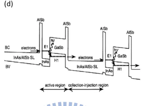
Mid-IR lasers with wavelengths beyond 3m are achievable using type-II QWs and interband cascade active region. The type-II QWs have staggered band edge alignment to the surrounding barriers, thus only one kind of carriers is confined inside the QWs and the other one is located in the region of the barrier layers. Figure 1.3(b) shows the band alignment of electron confined type-II QW lasers [7]. The optical transition takes place by recombination of the spatially separated electrons and holes. However the reduced electron-hole wavefunction overlap causes the optical oscillator strength to reduce, hence resulting a small optical gain, which limits the laser performance. The type-II “W” QWs were proposed and demonstrated by the research group of Naval Research Laboratory (NRL) in 1995. The “W” structure, as shown in Fig. 1.3(c), confines holes in the center GaInSb QW and electrons in the coupled two InAs QWs formed by the surrounding AlSb barrier layers to increase the
6
electron-hole wavefunction overlap [8]. The “W” configuration preserves two dimensional density states for both carriers and can suppress the Auger processes. The type-II “W” QWs lasers with emission wavelengths in the range of 3-7.3 m by optical pumping were reported, and an electrical injected laser using five periods of the “W” QWs emitting at ~3.5m in CW operation up to T=218K has been demonstrated [14-17].
Fig 1.3(a) Band alignments and fundamental electron-hole optical transition of type-I, and (b) type-II QW lasers [ref. 7].
7
Interband cascade lasers are promising for the wavelength range of 3-4m. Optical gain is realized through a sequential cascade processes in such structure, as shown in Fig. 1.3 (d). Electrons enter from the InAs/AlSb supper lattice (SL) injection region, and then resonantly tunnel into InAs QW region, in which then undergo an optical transition to the adjacent GaSb valence band states (in other words, a recombination process with holes in the GaSb layer). This transition is made possible due to the large band edge offset at the GaSb/AlSb interface. Finally, by using the broken-gap alignment carriers are able to resonantly tunnel back to the next collection/injection region rapidly (with rate ~0.1 ps). The processes repeat in the following periods. The interband quantum cascade laser emitting at 3.8-3.9 m operated at 210K in pulsed mode with the differential quantum efficiency >460%, and peak output power > 4W/facet was reported [18]. “W” type QWs have been used in interband cascade lasers for better performance. In 2008, the first above RT CW operated interband cascade laser with
Fig 1.3(c) Band alignment along with ground state electron and hole wavefunctions of type-II “W” structure QWs. (d) Band profile (not to scale) under bias of an interband quantum cascade active region and also indicated with the carrier optical transition in the AlSb/InAs/GaSb quantum well [ref. 8].
8
5-stage “W” QWs design emitting at 3.75m has been reported [19]. With further optimization, a record of 59mW CW output power with a 3.4% wall plug efficiency at 300K for such devices have been obtained [20]. By varying the thickness of InAs in “W” QWs, the interband cascade lasers have been demonstrated accurate lasing wavelength tuning in the region of 3-4 m, which could facilitate practical implementations [21].
We restrict ourselves in this brief review for interband transition active region lasers; therefore the part of intraband cascade lasers is not included here. Intraband cascade lasers are suitable for even longer wavelengths (> 4m). However, it is hard to fabricate due to the difficulties of requiring thickness controllability in few monolayers and up to thousands of sharp interfaces among layers. Besides, a high voltage is needed as operating the device, which generates lots heat cross the junctions, thus extra thermal management is always needed.
1.3 Research motivation
GaSb and InAs substrates are conventionally used for the development of mid-IR lasers. However, they are more expensive, with lower thermal conductivity and immature process technology as comparing to more popular substrates such as GaAs and InP. Thus, replacing the platform toward GaAs or InP substrate is highly desirable for the fabrication of mid-IR lasers. However, Sb-based mid-IR laser structures has large lattice mismatch between GaAs or InP substrate, which generates dislocation and degrades the laser performance. The method of inter facial misfit (IMF) arrays grown by MBE has been employed to reduce threading dislocations of lattice-mismatched GaSb-based mid-IR lasers on Si and GaAs substrates. Room temperature CW operated lasers emitting at 2m and ~2.2m have been demonstrated respectively on Si and GaAs substrates by Reboul and Rodriguez et al. [22, 23]. A thick
9
InAlSb buffer layer (~8 m) has been used by Nash et al. to eliminate defects for InGaSb QW mid-IR laser grown on GaAs substrate, which has 3.3m emission wavelength in pulse operation up to 219K [24].
InP-based material remains a relatively unexplored area in terms of interband mid-IR lasers. Type-I QW with emission wavelength longer than 2 m on InP is difficult due to lattice mismatch. The longest wavelength reported is 2.33 m with a highly strained InAs/InGaAs system [25]. However, if we use the type-II InGaAs/GaAsSb heterostructure on InP substrates, we can bypass the requirement for small band gap materials by using the staggered band alignment and therefore the wavelength can be extended longer without being limited by the band gaps of the constituent materials. The “W” type QWs with the type II staggered band alignment using InGaAs/GaAsSb have been shown to be able to extend the lasing wavelength in the mid-infrared range [26-29]. Thanks to the development of 1.3 and 1.55 m lasers for fiber communication applications. InP-based system has very mature process technologies including regrowth of devices. Mid-IR optoelectronics using type-II InGaAs/GaAsSb hetero-structure on InP substrates have caught attention recently [30, 31].
This dissertation is aimed to investigate type-II InGaAs/GaAsSb “W” type QWs on InP substrates in both theory and experiments, and then to design and fabricate the mid-IR lasers with “W” type QWs. The organization of this dissertation is described in the following section.
1.4 Organization of this dissertation
Chapter 2 presents theoretical studies of the “W” type structure of QWs. The nature of the tradeoff between extending of wavelength and optical oscillation strength is analyzed by the results of calculations based on simple one-band effective mass approximation. The E-k band structures of “W” QWs are simulated by using the 8-band k.p theory to look more insight to
10
the characteristics like band edge effective masses and momentum matrix elements. The results lead to calculations of optical gain based on basic laser theorem, which can be treated as a design guideline of “W” laser active region.
Chapter 3 presents experimental techniques including how to prepare samples, material analysis methods, and device measurement setups. Our samples are grown by a MBE system. X-ray diffraction helps to understand the lattice constant of epi layers. Photoluminescence (PL) studies could characterize the type-II nature of grown samples. And the apparatus to measure optically pumped “W” mid-IR lasers will be detailed.
Chapter 4 describes PL experiment results of the designed samples, which will be compared and found consistent with theoretical predictions. The peak of emission wavelength shifting to short wavelength as increasing PL excitation power (Pex) reveals the nature of
type-II structure; however which does not follow the Pex 1/3 law as described in published
literature. This observation will be discussed more and reasonably explained by a proposed model.
Chapter 5 describes the structure of the designed “W” QWs mid-IR laser along with the waveguide calculation. The lasing results are demonstrated via optical pumping experiments. Studies of different laser cavity lengths and operation temperatures are implemented to analyze “W” lasers. Laser performance related parameters such characteristic temperature (T0)
and internal loss (i) are extracted. It also includes a detailed discussion of Auger process and an estimation of Auger coefficient, which are important for mid-IR lasers.
11
Chapter 2
Theoretical studies of InGaAs/GaAsSb type-II “W” type quantum
wells on InP substrates
The type-II InGaAs/GaAsSb heterostructure has staggered band alignment that offers a good strategy for developing mid-IR light sources on InP substrates. The “W” type structure introduces barrier layers for better electron confinement and carriers wavefunction overlap and hence optical oscillator strength. This chapter gives the theoretical view of the “W” structure. One band effective mass approximation provides a simple way to study the trade-off nature of “W” type QWs, longer emission wavelength accompanied with reduced wavefunction overlap. More deliberate calculations are carried based on the 8-band k.p theory, which eventually leads to optical gain calculations for needs of design considerations of “W” mid-IR lasers. The gain spectra and their peak values at various carrier densities were calculated. We have found that a more balanced electron and hole masses in the type-II “W” QWs can benefit the material gain. In our designed cases, we have seen that the reduced hole effective mass due to a higher Sb content can partially compensate the gain loss caused by the reduced transition matrix element. Based on the optimized design, a material gain above 103 cm-1 is readily achievable for a single properly designed “W” quantum well. In order to be self-contained, all simulation parameters used will be listed as completely as possible.
2.1 Band alignments of “W” type quantum well
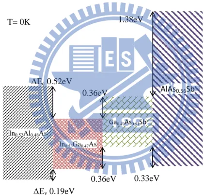
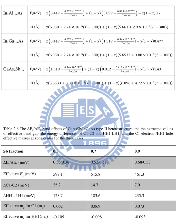
Four kinds of ternary semiconductors can be lattice matched to InP substrate with a lattice constant of 5.87Å , which are InAlAs, InGaAs, GaAsSb, and AlAsSb. Table 2.1 lists their
12
alloy compositions and band gaps. Their band alignments together with band offset values are depicted in Fig. 2.1, which are based on experiment results in literatures[32-34].
In this material system, the two narrower bandgap materials, InGaAs and GaAsSb, form a type II heterjunction. The transition between the conduction band state in InGaAs and the valence band state can give out light emission with wavelength longer that the direct band-to-band transition in individual materials. Based on the band offset, the energy
In0.52Al0.48As In0.53Ga0.47As GaAs0.49Sb0.51 AlAs0.56Sb0.44 - direct band gap (eV) 0K 1.51 0.81 0.81 2.5 300K 1.42 0.73 0.72 2.4
Table 2.1 Room temperature (300K) and low temperature (0K) direct band gaps of ternary alloys lattice matched to InP substrate.
1.38eV ΔEc 0.52eV ΔEv 0.19eV 0.36eV In0.52Al0.48As In0.53Ga0.47As Ga0.49As0.51Sb AlAs0.56Sb 0.36eV 0.33eV T= 0K
Fig 2.1 Band lineups, with values of conduction and valence band offsets (ΔEc and ΔEv)
indicated, of the four ternary alloys lattice matched to InP substrate.
13
difference between the conduction band edge of InGaAs and the valence band edge of GaAsSb is ~0.5eV, which can generate a ~2.5 m light emission [35]. The two wider bandgap materials, InAlAs and AlAsSb, form type-I heterojunctions with the two narrower bandgap materials and can be used as barrier layers for carrier confinement. The emission wavelength can be further extended by increasing either the indium content in InGaAs alloy or the antimony fraction in GaAsSb alloy. To better understand this, the band edge evolutions by altering the alloy compositions will be described in next paragraph.
The calculations are based on the “model-solid” theory, which uses deformation potentials to predict behavior of band offsets in either lattice matched or pseudomorphic layers[36, 37]. Here only gives the case that normal directions of ternary alloys are all along [001]. In the condition without strained, the lattice constant (a0) of a ternary alloy AxB1-xC is assumed to
follow the Vegard law and estimated from the lattice constants of two binary constituents. a0_A𝑥B1−xC = x a0_AC + (1 − x) a0_BC , (2.1.1)
Band gap (Eg), spin-orbit split-off energy (Δ0), average valence band edge (Evav), i.e. the
average of the heavy-hole, light-hole, and spin-orbit split-off bands (Ehh+Elh+Eso)/3, and other
parameters of the ternary are assumed fitted to a simple empirical quadratic formula:
PA𝑥B1−xC = x PAC+ (1 − x)PBC− x (1 − x)𝐶𝐴𝐵𝐶 , (2.1.2) where P represents an arbitrary semiconductor parameter, and C is so called the bowing parameter, which accounts for the deviation from a linear interpolation of the two constituent binaries. In general, the band gap bowing parameter of ternary alloy is negative, which means the ternary band gap is always smaller than the linear interpolation result. The reason can be originated to the disorder effect formed by the presence of different cations or anions. Conduction band (Ec) and valence band (Ev) of the alloy can be described as:
Ev = Ehh = Elh= 𝐸𝑣𝑎𝑣 + ∆0/3, (where Ehh and Elh degenerated) (2.1.3) Ec = Eg+ Ev. (2.1.4)
14
A pseudomorphic layer implicates a thin epi layer that can bear the lattice mismatch by subjecting its in-plan lattice constant to the underneath host material. The strain, expressed by biaxial strain ε|| and uniaxial strain ε┴ described below, held within the pseudomorphic layer
could change its electronic properties: ε
|| = (as− a0)/a0, (2.1.5)
ε┴= −2CC12
11 ε||, (2.1.6)
where as and a0 denote substrate lattice constant and unstrained alloy lattice constant. C12
andC11 refer to material elastic constants. ε|| isnegative/positive when the pseudomorphic
layer is under compressive/ tensile strain.
The shift of band edge levels caused by strain effects can be divided into two components, one of which is hydrostatic contribution and the other is shear contribution. The former push outward (pull inward) conduction and valence band edges from band gap center as the epi layer under compressive (tensile strain). The later splits energy levels of heavy hole and light hole bands at Г point. Now conduction and valence band edges can be expressed as :
E𝑣 = VBO + ∆𝐸𝑣𝑎𝑣ℎ𝑦 + max(∆𝐸ℎℎ𝑠ℎ, ∆𝐸
𝑙ℎ𝑠ℎ), (2.1.7)
𝐸𝑐 = VBO + 𝐸𝑔 + ∆𝐸𝑐ℎ𝑦, (2.1.8)
VBO = 𝐸𝑣𝑎𝑣 + ∆0/3. (2.1.9) where ∆𝐸𝑣𝑎𝑣ℎ𝑦 and ∆𝐸𝑐ℎ𝑦 account for hydrostatic components,
∆𝐸𝑣𝑎𝑣ℎ𝑦 = av (2ε||+ ε┴), (2.1.10) ∆𝐸𝑐ℎ𝑦 = ac (2ε||+ ε┴), (2.1.11) av/ac refers to hydrostatic deformation potentials for conduction/valence bands.
The max(∆𝐸ℎℎ𝑠ℎ, ∆𝐸𝑙ℎ𝑠ℎ) in equation (2.1.7) means only select the maximum term between the ∆𝐸ℎℎ𝑠ℎ and ∆𝐸
𝑙ℎ𝑠ℎ. The shear contribution couples to spin-orbit interaction and can be
15
∆𝐸ℎℎ𝑠ℎ = −𝑏(ε┴− ε|| ), (2.1.12)
∆𝐸𝑙ℎ𝑠ℎ = 1/2(−∆
0+ 𝑏(ε┴− ε|| ) + √∆02+ 2∆0𝑏(ε┴− ε||) + 9𝑏2(ε┴− ε||)2 [37], (2.1.13)
where b is the tetragonal deformation potential.
Fig. 2.2 is depicted below for better understanding of strain effects induced energy shift of energy levels. In general, if pseudomorphic layer is biaxial compressive-strained, ∆𝐸ℎℎ𝑠ℎ will be larger than ∆𝐸𝑙ℎ𝑠ℎ and make heavy hole band shifted above light hole band. In the tensile-strained case ∆𝐸𝑙ℎ𝑠ℎ>∆𝐸ℎℎ𝑠ℎ and light hole is above heavy hole band.
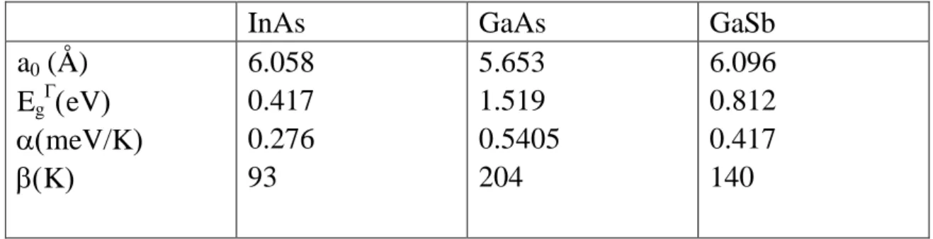
Band structure parameters for binary semiconductors of InAs, GaAs, and GaSb are listed in Table 2.2(a), including and which are used to empirically fit binary band gap as a function of temperature, ∆𝑬𝒉𝒉𝒔𝒉 + ∆𝑬 𝒗𝒂𝒗 𝒉𝒚 Eg= Ec- Ev Evav Ev
E
c Unstrained Lattice constant: a0 Δ0/3 Evav+∆𝑬𝒗𝒂𝒗𝒉𝒚 Compressive-strained Δ0/3+∆𝑬𝒉𝒉𝒔𝒉 Substrate lattice constant: as ∆𝑬𝒄𝒉𝒚 Evav+∆𝑬𝒗𝒂𝒗𝒉𝒚 Tensile-strained Δ0/3+∆𝑬𝒍𝒉𝒔𝒉 ∆𝑬𝒄𝒉𝒚Fig 2.2 Strain effects induced band edge shifts for the three cases: tensile-strained, unstrained, and compressive-strained.
∆𝑬𝒍𝒉𝒔𝒉+ ∆𝑬
𝒗𝒂𝒗 𝒉𝒚
16
Table 2.2(a) Band structure parameters for binary semiconductors of InAs, GaAs, and GaSb.
E𝑔 ( ) = Eg−
2
+ (2.1.14) Bowing parameters of InGaAs and GaAsSb ternary semiconductors are listed in Table 2.2(b). These values of parameters are from the literature [4]. Other material parameters also can be found there, while only most related InGaAs/GaAsSb ternaries are presented here. It is known the material parameter values are varied among references and should be treated within a certain range. However we use the exact values suggested by the literature without tuning, because the purpose of our simulations, including the latter k.p calculations, is to study overall tendency and characteristics of the “W” QWs as the structure parameters, such as layer thickness and alloy composition, are varied and not intended to fully match with experiment results. Fig. 2.3(a) and Fig. 2.3(b) show the calculation results of the amount of band edge shifts for InGaAs and GaAsSb pseudomorphic layers on InP substrate caused by varying indium fraction and antimonite fraction respectively. In order to see explicitly the energy shifts of conduction band (CB) edge of InGaAs and valence band (VB) edge of GaAsSb, their energy values have been reset to zero when they are lattice matched to InP substrate. Notice that, CB edge of InGaAs drops as increasing indium fraction, while VB edge of GaAsSb goes up as increasing antimony fraction. Either of them leads to decrease energy difference between CB edge of InGaAs and VB edge of GaAsSb for InGaAs/GaAsSb heterostructure, and hence helps to extend emission wavelength.
InAs
GaAs
GaSb
a
0(Å )
E
g
eV
meV/K
K
6.058
0.417
0.276
93
5.653
1.519
0.5405
204
6.096
0.812
0.417
140
17 Table 2.2(b) Bowing parameters for InGaAs and GaAsSb.
Fig. 2.3(a) Energy shifts of band edges, including conduction (Ec), heavy hole (Ehh), and light hole
(Elh) bands, vs. indium fraction for InGaAs pseudomorphic layer, and Fig. 2.3(b) those for GaAsSb
pseudomorphic layer with varied antimony fraction on InP substrate.
VBO
eV
∆
0
eV
a
c
eV
a
v
eV
b
eV
-0.59
0.39
-5.08
1
-1.8
-0.8
0.341
-7.17
1.16
-2.0
-0.03
0.76
-7.5
0.8
-2.0
C
Gpa
C
12
Gpa
832.9
452.6
1221
566
884.2
402.6
InGaAs
GaAsSb
E
g
eV
VBO
eV
∆
0
eV
0.477
-0.38
0.15
1.43
-1.06
0.6
0.0 0.2 0.4 0.6 0.8 1.0 -0.8 -0.6 -0.4 -0.2 0.0 0.2 0.4 0.6 0.8 1.0 1.2 Elh E hh Energy (eV) Antimony fraction Ec GaAs 0.51Sb0.49 lattice-matched to InPGaAs1-xSbx pseudomorphic layer
(b) 0.0 0.2 0.4 0.6 0.8 1.0 -0.8 -0.6 -0.4 -0.2 0.0 0.2 0.4 0.6 0.8 1.0 1.2 E lh E hh Energy (eV) Indium fraction E c In0.53Ga0.47As lattice-matched to InP In xGa1-xAs pseudomorphic layer (a)
18
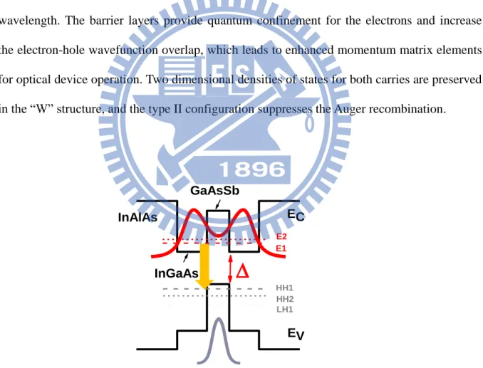
A typical band alignment of the “W” type QW along with the electron and hole fundamental wavefunctions are shown in Fig. 2.4. The “W” structure mainly consists of symmetric InGaAs/GaAsSb/InGaAs layers sandwiched by InAlAs barrier layers. The structure gains the name from the “W”-like shape of conduction band profile. Because of the type-II band alignment, holes are confined inside the valence band (VB) of GaAsSb QW, forming heavy hole (HH) and light hole (LH) sub-bands, and electrons are confined in the two coupled InGaAs QWs, which have the split symmetric (E1) and the anti-symmetric (E2) states. The fundamental E1-HH1 optical transition has a smaller effective band gap energy not limited by the bandgaps of the constituent layers, and therefore gives a longer emission wavelength. The barrier layers provide quantum confinement for the electrons and increase the electron-hole wavefunction overlap, which leads to enhanced momentum matrix elements for optical device operation. Two dimensional densities of states for both carries are preserved in the “W” structure, and the type II configuration suppresses the Auger recombination.
Fig. 2.5 shows the relative position of the band edges of the materials used in the “W” QW,
E2 LH1 HH2 HH1 E1 EV GaAsSb InGaAs InAlAs
ECFig. 2.4 A Scheme of a typical band alignment for the “W” type QW along with fundamental electron and hole wavefunctions based calculations of one band effective mass model.
19
Fig. 2.5 Band edge energy levels (conduction band edge Ec denoted by solid line and valence band
edge Ev by dashed line) of In0.53Ga0.47As and In0.52Al0.48As which are lattice matched to InP substrate,
and GaAs1-xSbx pseudomorphic layer with Sb fraction varied from 0 to1. The biaxial strain is
indicated on the top horizon axis. The band gap values for each material are indicated by the arrows. The Δ denotes the energy separation between the Ec of In0.53Ga0.47As and the Ev of In0.53Ga0.47As
including In0.53Ga0.47As and In0.52Al0.48As which are lattice matched to InP substrate, and The
Sb mole fraction in GaAs1-xSbx is varied from 0 to 1. The top horizontal axis indicates the
biaxial strain in the GaAsSb layer, which is assumed to be pseudomorphically grown with the same in-plane lattice constant as InP. The plot of band edge energy shifts of GaAsSb are calculated based on “model solid” theory same as Fig. 2.3(b) but takes an offset to meet consistency with the band lineup for lattice matched case (GaAs0.51Sb0.49) depicted in Fig. 2.1.
The energy difference (Δ) between CB edge of In0.53Ga0.47As and VB edge of GaAsSb shrinks
as the Sb fraction, x, increases. It is only around 0.25eV when x is 0.8. This energy corresponds to a very respectable 4.96 m mid-IR light emission (without adding the electron and hole quantized energies). In next section, emission wavelength and wavefunction overlap of “W” QWs with varied structure parameters, including thickness of InGaA and GaAsSb and Sb fraction of GaAsSb, will be simulated by simple one band effective mass approximation.
0.0 0.2 0.4 0.6 0.8 1.0 -0.5 0.0 0.5 1.0 1.5 4 3 2 1 0 -1 -2 -3 -4 c v In0.53Ga0.47As GaAs1-xSbx Energy(eV) Sb fraction x In0.52Al0.48As
GaAsSb strain (%)20
2.2 The tradeoff feature for the “W” type quantum well explored
by one band effective mass approximation
One band effective mass approximation provides basic way to calculate quantized energy levels and wavefunction profile for quantum structure, which is time saving for computation so that it can be used to simulate cases with various structure parameters to reveal overall behaviors. Once knowing band alignment values of “W” structure in early section, electron and hole confinement energies are computed by solving one band Schrödinger wave equation with conduction band effective mass and valence band effective mass respectively. It also needs to fit proper boundary conditions for wavefunction across hetero interfaces described below. Conduction band: 2𝑚−ℏ2 0 ∇ 1 𝑚𝑐∗∇ϕ𝑒+ 𝐸𝑐 = 𝐸𝑛𝑐ϕ𝑒, (2.2.1) Valence band: −ℏ2 2𝑚0 ∇ 1 𝑚𝑣∗∇ϕℎ+ 𝐸𝑣 = 𝐸𝑚𝑣ϕℎ, (2.2.2) Boundary conditions: ϕ𝑒,ℎ|ℎ𝑒𝑡𝑒𝑟𝑜+ = ϕ𝑒,ℎ|ℎ𝑒𝑡𝑒𝑟𝑜− (2.2.3) 1 𝑚𝑐,𝑣∗ ∇ϕ𝑒,ℎ|ℎ𝑒𝑡𝑒𝑟𝑜 + = 1 𝑚𝑐,𝑣∗ ∇ϕ𝑒,ℎ|ℎ𝑒𝑡𝑒𝑟𝑜 − (2.2.4)
Notations: 𝑚0 : Free electron mass
𝑚𝑐∗/𝑚𝑣∗ : Conduction band/valence band effective mass divided by 𝑚0
ϕ𝑒/ϕℎ : Electron / hole wavefunction
𝐸𝑐/𝐸𝑣 : Conduction/ valence band edge potential profile 𝐸𝑛𝑐/𝐸𝑚𝑣 : Conduction/ valence band quantum confined levels ℏ : Reduced plank constant
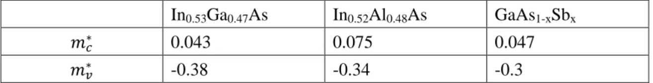
The effective mass values used for simulations are listed in Table 2.3. For simplicity, the effective mass for GaAsSb remains the same value without considering changes contributed
21
by strain effect and different composition. Calculations were performed with InGaAs and GaAsSb thickness varied from 2nm to 7 nm, and with Sb fraction of GaAsSb varied from 0.5 to 0.9. We used In0.52Al0.48As as the barrier material in our “W” structure, which has a higher
conduction band offset as compared to the (Ga)InP layer used in ref. 28 and the GaAsSb layer used in ref. 29. Our structure has a better electron confinement and a higher energy level when the same InGaAs width is used in the structure. In this parameter range, the ground state of valence band is always from heavy hole band because of the compressive strain of GaAsSb layer, which splits heavy hole band above light hole band, and the heavier effective mass of heavy hole as compared to light hole band makes the first heavy hole confined level more deeper. One can deduce the emission wavelengths of ground states optical transitions (E1 to HH1) and their corresponding electron-hole wavefunction overlaps. The square of wavefunction overlap is known to proportional to optical transition rate. Figure 2.6(a) shows the 3D contour plot for the three chosen wavelengths of 2m, 2.5m, and 3m, where the x, y, and z axes are, in turn, values of the InGaAs layer width, GaAsSb layer width, and Sb mole fraction in GaAsSb. Figure 2.6(b) shows their corresponding wavefunction overlap square displayed in in grayscale, where the brightness increases with the magnitude. The maximum and minimum values in the plot are 0.261 and 0.015 respectively.
In0.53Ga0.47As In0.52Al0.48As GaAs1-xSbx
𝑚𝑐∗ 0.043 0.075 0.047
𝑚𝑣∗ -0.38 -0.34 -0.3
As shown in Fig. 2.6(a), wavelength can be tuned in the range from 2 to 3m via modifying by varying the three parameters mentioned above. However, as the wavelength is increased
22
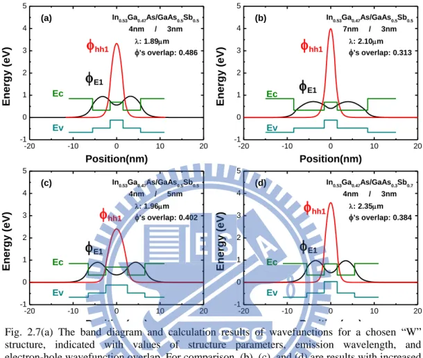
the wave function overlap decreases resulting in a smaller matrix element. A gradual increase in darkness in the plot is clearly seen as the wavelength changed from 2m to 3m in Fig. 2.6(b). This is a trade-off between the long wavelength emission and the optical matrix element and it is an intrinsic feature for the “W” type QW. The electron and hole are confined separately in different layers, the electron in the two coupled InGaAs layers and the hole in the GaAsSb layer, as shown in Fig. 2.4. Since the confinement potentials are large (~0.4eV) for both carriers, the quantization energies are decided by their own layer thickness; a thicker InGaAs or GaAsSb layer leads to a smaller electron or hole quantization energy and hence a longer emission wavelength. Although the increase of the InGaAs or GaAsSb layer thickness extends the emission wavelength, it also makes the electron and hole wave functions more concentrated in individual layers, and causes the reduction of electron-hole wavefunctions overlap. A similar trade-off exists when the Sb content in the GaAsSb layer is varied. The wavelength can be extended longer with a higher Sb content due to the reduced energy separation, Δ indicated in Fig 2.5, between the electron and the hole states. The raised conduction band edge, however, blocks the electron wave function penetration into the GaAsSb layer causing a reduction of the electron-hole wave function overlap. In order to a better elucidation, Fig. 2.7 (a) gives the wavefunctions at a chosen “W” structure indicated with values of ground state wavelength emission and overlap, and for comparisons, Fig. 2.7(b), Fig. 2.7 (c) ,and Fig. 2.7 (d) give the cases with each varying thickness of InGaAs, GaAsSb, and Sb fraction respectively.
As shown in Fig. 2.6(a), there are many possibilities in choosing the layer parameters to achieve the same emission wavelength. However, a different combination of the three parameters has a different strength in the transition matrix element. Looking carefully at Fig. 2.6(b), one can see that a better optical gain is generally obtained with a higher Sb mole fraction and thinner InGaAs/GaAsSb layers even for the same wavelength. Given such design
23
flexibility, one has to be careful, however, when using a high Sb content in the GaAsSb layer because the material quality may degrade.
(a)
Wavelength 3D contour plots(b)
| Wavefucntion overlap |2Fig. 2.6(a) 3D contour plots and (b) corresponding wavefunction overlap square displayed in correlated grayscale at three wavelengths based on calculations using the one-band effective mass approximation.
24 -20 -10 0 10 20 -1 0 1 2 3 4 5 Energy (eV) Position(nm) (b) In0.53Ga0.47As/GaAs0.5Sb0.5 7nm / 3nm : 2.10m 'soverlap: 0.313 Ec Ev
E1
hh1 -20 -10 0 10 20 -1 0 1 2 3 4 5
hh1 Energy (eV) Position(nm)
E1 : 1.89m 'soverlap: 0.486 In0.53Ga0.47As/GaAs0.5Sb0.5 4nm / 3nm (a) Ec Ev -20 -10 0 10 20 -1 0 1 2 3 4 5 Energy (eV) Position(nm) (c) In0.53Ga0.47As/GaAs0.5Sb0.5 4nm / 5nm : 1.96m 'soverlap: 0.402 Ec Ev
E1
hh1 -20 -10 0 10 20 -1 0 1 2 3 4 5 Ev Energy (eV) Position(nm) In0.53Ga0.47As/GaAs0.3Sb0.7 4nm / 3nm : 2.35m 'soverlap: 0.384 (d) Ec
E1
hh1Fig. 2.7(a) The band diagram and calculation results of wavefunctions for a chosen “W” structure, indicated with values of structure parameters, emission wavelength, and electron-hole wavefunction overlap. For comparison, (b), (c), and (d) are results with increased thickness of InGaAs, GaAsSb, and Sb fraction of GaAsSb respectively. By comparing to (a), each shows a trade-off behavior, Extending wavelength accompanying with the reduction of wavefunction overlap.