行政院國家科學委員會專題研究計畫 成果報告
高精度與低製程、電壓、溫度變異敏感度之脈衝擴展式時 間至數位轉換器及其應用(I)
研究成果報告(精簡版)
計 畫 類 別 : 個別型
計 畫 編 號 : NSC 96-2221-E-011-151-
執 行 期 間 : 96 年 08 月 01 日至 97 年 10 月 31 日 執 行 單 位 : 國立臺灣科技大學電子工程系
計 畫 主 持 人 : 陳伯奇
計畫參與人員: 碩士班研究生-兼任助理人員:陳柏宇 碩士班研究生-兼任助理人員:陳怡瑾 碩士班研究生-兼任助理人員:胡孝慈 碩士班研究生-兼任助理人員:彭郁涵 碩士班研究生-兼任助理人員:王堉鋅 碩士班研究生-兼任助理人員:陳首志
報 告 附 件 : 出席國際會議研究心得報告及發表論文
處 理 方 式 : 本計畫涉及專利或其他智慧財產權,2 年後可公開查詢
中 華 民 國 97 年 09 月 29 日
行政院國家科學委員會補助專題研究計畫成果報告
※※※※※※※※※※※※※※※※※※※※※※※※※※
※
高精度與低製程、電壓、溫度變異敏感度之脈衝擴展式※
※
時間至數位轉換器及其應用※
※※※※※※※※※※※※※※※※※※※※※※※※※※
計畫類別:■個別型計畫 □整合型計畫 計畫編號: NSC 96-2221-E-011-151
執行期間: 96 年 8 月 1 日至 97 年 7 月 31 日
計畫主持人:陳 伯 奇 共同主持人:
計畫參與人員:陳柏宇、陳怡瑾、胡孝慈、彭郁涵、王堉鋅、陳首志
執行單位:台灣科技大學電子工程系
中 華 民 國 97 年 7 月 1 日
高精度與低製程、電壓、溫度變異敏感度之脈衝擴展式時間至數位轉換器及其應用
A High Accuracy Low PVT Sencitivity Pulse-Stretching Time-to-digital Converter and Its Applications
計畫編號:NSC 96-2221-E-011-151 執行期間:96 年 8 月 1 日 至 97 年 7 月 31 日 主持人:陳伯奇 台灣科技大學電子工程系 教授
一、 中文摘要
本計劃提出一個無量測範圍限制、具自我校準脈 衝擴展器之高精度時間至數位轉換器(Time-to-digital converter,簡稱 TDC),希望藉由自動校準的方式,來 降低環境溫度變異、製程參數變異以及工作電壓的改變 所造成量測上的誤差,大幅提高時間至數位轉換器之準 確度。
在一般的應用上,高精度、高解析能力、低環境變 異的 TDC 電路,可用來製作一些需低誤差的電路需 求,比如說可攜式的雷射測距儀或溫度量測器等,其解 析度必須不易受外在環境影響;而且有鑒於積體電路迅 速的發展,更加可以彰顯本電路價格便宜、特性好以及 容易使用等諸多優點,使其更具發展價值。
本電路的解析度高達 19.53ps,以 TSMC 0.35um 2P4M 製程實現,晶片面積不含輸入/輸出墊(I/O Pad) 為 0.5mm2。利用單擊觸發方式,範圍在 0.4ns~11ns 且 量 測 間 距 為 400ps 的 情 形 下 , 測 得 的 INL 只 有 +0.5LSB~-0.5LSB。而在量測頻率為 0.2/sec 之情形下,
其消耗功率為 19.8mW。
英文摘要
A highly accurate time-to-digital converter (TDC) based on self-calibrated pulse stretcher has been presented to own a theoretically unlimited input range. Through self calibration, the inaccuracy caused by process, voltage and temperature variations can be eliminated to enhance the performance of the TDC substantially.
The high accuracy, high resolution and low PVT sensitivity of TDC are required by many applications, such
as portable laser range finders and digital thermometers. It will make the proposed circuit more and more popolar in the future.
The test chips have been fabricated in a TSMC 0.35-um 2P4M standard digital CMOS process. The resolution of the proposed TDC is measured to be as fine as 19.53ps with a reference clock of 100MHz and the chip area is merely 0.78mm×0.645mm, excluding the I/O pads.
By true single shot measurements, the INL is within +0.5LSB~-0.5LSB for 0.4ns to 11ns input range from with 400ps steps. The power consumption is 19.8mW at 0.2 samples/s measurement rate.
二、 計畫的緣由與目的
近年來對於交通工具導航與防撞系統的小型雷射 雷達之研究的蓬勃發展。高解析度而快速的時間量測功 能是雷射雷達系統中極為重要的一環。時間至數位轉換 器(TDC)的一個應用範例為全數位相位鎖定迴路或全 數位延遲鎖定迴路[1] (ADPLL, ADDLL),如圖 1.所 示,其中 TDC 取代相位比較器及充放電幫浦(Charge pump),利用 TDC 偵測兩波形(FREF and HCLK)之相位 差異,經低通率波後再控制後續之數位控制震盪器 (digital controlled oscillator)以振出所需要之標的頻率。
藉由高效能及高解析度 TDC 之助,可達到快速鎖定及 低抖動之目的。
一般而言對時間量測電路的要求不外乎下列幾 項:1)高解析度 2)足夠的量測範圍 3)快速的量測時間 4) 不受量測信號的頻率變動影響 5)高準確度 6)低功率、
低成本等等,傳統上時間至數位轉換器必須使用射極耦
合邏輯(ECL)的元件來實行,不但得占用非常大的電路 板,且消耗的功率高達數瓦以上,根本不適合用在可攜 式系統或系統晶片內[2-3]。
本計劃以計數器法之時間至數位轉換器為基礎,搭 配嶄新之自我校準雙斜率脈衝擴展器(Pulse Stretcher) 實現的內插器(interpolator),以達到將 PVT(process, voltage and temperature) 所造成的影響壓抑至最低,以 實現高解析度且又不受 PVT 變異影響之時間至數位轉 換器。
TDC
Loop Filter
DCO Phase
error FREF
N
HCLK
圖 1. 具 TDC 之全數位鎖相迴路
三、 研究方法及成果
3.1 計數器法之時間至數位轉換器
以計數器方法之時間至數位轉換器[4],其運作方 式最為直接,如圖 2.所示,為使用計數器設計方法之 TDC 時序圖,其設計方法與電路動作原理說明如下:
在開始量測時,首先由控制電路發送一個起始脈 衝,讓量測時間遮罩訊號為 ON,此時會迫使計數器進 入計數狀態;同樣地,在量測時間欲停止時,再由控制 電路送一個結束脈衝,使得量測時間遮罩訊號為 OFF,
此時計數器會停止計數。而在量測時間遮罩訊號為 ON 與 OFF 之間,計數器會不斷的計數,假設計數器輸入 的頻率為 F,週期為 Tclk,若最後計數之結果為 n,則 將參考信號週期乘上 n,可得到欲量測的時間結果如下 式(1)所示:
i n C L K
T = n × T ____(1) 此種 TDC 的優點為:
1.待測時間訊號量測範圍可以做的很大,條件為只要 計數器的輸出位元數夠多即可。2.若計數器的輸入參考 時脈訊號夠穩定且不易受干擾,TDC 也可擁有相當優 秀的線性特性。
Tin
TCLK
Start
Stop
Mask
TCLK
圖 2. 計數器設計方式之 TDC 時序圖 3.2 脈衝擴展法之時間至數位轉換器
上述計數器法之時間至數位轉換器是應用最普遍 的一種方法,它的優點是量測範圍大、線性度高,但此 方法在量測上有一個無法避免的問題,即 Start 和 Stop 脈衝信號並無法與輸入參考時脈同步,造成在量測的開 始及結束的地方都有些許的誤差產生,因此在西元 2000 有文獻提出以內插器(Interpolator)實現之脈衝擴展法之 時間至數位轉換器[5];而其架構如圖 3.所示,其主要架 構 包 含 時 間 至 脈 衝 控 制 電 路 (Time to Pulse Control Circuit)、兩組 n 位元內插器(n-bit Interpolator)、與三組 加 載 式 上 數 計 數 器 ; 其中一組為粗測計數器(Coarse Counter),另外兩組為細測計數器(Fine Counter)。
T1
n- bit Interpolator2
Digitized T1
Stop Start
TCLK Time to Pulse Control Circuit
n- bit Interpolator1
Coarse Counter T12
T2 Digitized T2
Digitized T12
Fine Counter 2
Fine Counter 1
圖 3. 脈衝擴展法之時間至數位轉換器方塊圖
TCLK
Start Stop T1
T2
T12
TCLK
Tin
圖 4. 脈衝擴展法之時間至數位轉換器時序圖
圖 4.即為此 TDC 之時序圖,若於外部送入 Start 和 Stop 兩訊信號,透過時間至脈衝控制電路來產生一個遮 罩信號 Tin,其中 Tin的寬度是從 Start 脈衝的正緣到 Stop 脈衝的正緣,其後,時間至脈衝控制電路(Time to Pulse Control Circuit)會將 Tin細分成三部份,分別是 T1、T2 和 T12,其中 T1、T2為兩組細測時間寬度,而 T12 是屬 於粗測時間寬度。粗測時間寬度為參考時脈(TCLK)週期 之整數倍,且交由粗測計數器去計數,而細測時間寬度 則送入兩組 n-bit 內插器,之後所得之兩組數位值再分 別交由細測計數器計數。因此從此時序圖,我們初步可 得 知 其 輸 入 時 間 Tin 可 表 示 為 下 式 (2):
2 1
12 T T
T
Tin = + − ____(2) 此時若假設內插器的內插因子(Stretching Factor)
為 M,而兩組細測時間寬度 T1、T2分別輸入內插器之 後,所得到的數位輸出值為 D1、D2,且粗測時間寬度 經由計數器的計數結果為 D12,此部分將於 3.4 節詳細 探討。因此,我們可得出最後之輸入時間寬度 Tin可表 示如下式(3):
M D T M D T T D
Tin= 12× clk+ 1× clk − 2× clk
M D T D T
D12× clk + ( 1− 2) clk
= ____(3) 倘若只有一組細測時間,意味著整個電路只有一組
內插器,其架構就如我們在先前 2.4.2 章節所談到之雙 斜率法,當單一組內插器如有任何的偏移(offset),將會 直接反應在細測時間的數位輸出值 DL,如下式 (3.3),
其造成量測到的時間寬度包含偏移量。
1 2
c lk
in c lk L
T D T D T
= × + × M ____(4) 此外,採用兩組內插器,還可額外增加一個去除時
間至脈衝控制電路偏移(offset)的好處,由於 T12與 T1、 T2間的分割很難做得完全精準,其間的誤差便會造成 整體測量的輸出偏差,解決之道在於儘量將時間至脈衝 控制電路控制 T1、T2 產出的邏輯閘佈局做到彼此匹 配,如此一來 D1、D2的偏差便可在公式(3)中對消,提 升測量的準確度。
3.3 具高精度自我校準脈衝擴展器之時間至位轉換器 上述脈衝擴展法之時間至數位轉換器原理,在此論
文我們提出了具有自我校準之脈衝擴展器之時間至數 位轉換器,架構圖如下圖 5.所示,其中包含了時間至脈 衝控制電路(Time to Pulse Control Circuit)、兩組具有自 我 校 準 之 n-bit 內 插 器 (n-bit Interpolator with Self-calibration)以及與一般之脈衝擴展法之時間至數位 轉換器相同之三組加載式上數計數器,也分別為兩組細 測計數器和一組粗測計數器。其中,由於每個內插器皆 配備專屬之自我校準電路,因此我們期望於校準循環 (Calibration Cycle)時將擴展因子調整到原始設計值,而 後便可轉入量測循環(Measurement Cycle),進行待測時 間之測量工作。此外,為了加速自我校準電路的運行,
循序逼近式(SAR, Successive Approximation Register)之 校準方式將成為此 TDC 的首選[6-8]。而其整體時序圖 與一般脈衝擴展法之時間至數位轉換器大同小異,就承 如式(2)、(3)之結果,因此以下章節將探討整個 TDC 之 細部電路之動作原理,以及其校準原理。
T1 Digitized T1
Stop Start
TCLK Time to Pulse Control Circuit
Interpolator1 with Self-calibration
Coarse Counter T12
T2 Digitized T2
Digitized T12
Fine Counter 2
Fine Counter 1 n-bit
Interpolator2 with Self-calibration
n-bit
圖 5. 自我校準脈衝擴展法之時間至數位轉換器方塊圖 3.4 模擬及量測結果
本晶片以 TSMC 0.35um CMOS 製程製作,圖 6.為 其 晶 片 之 顯 微 圖 , 不 含 I/O PAD 之 面 積 為 645um×780um。
為方便計算及後續處理,所有長、短區間之差分非 線性誤差及整體非線性誤差皆由 Matlab 處理,並繪製 成圖 7.所示。電壓變異量測在 2.8V~3.6V 的範圍內,解 析度最大為 19.855ps 最小為 19.48ps;溫度變異量測在 -20~100 oC 的範圍內,解析度最大為 19.695ps,最小為 19.428ps,量測結果彙整於圖 8.,電路之規格列於表 1.。
Cap Cap
SAR SAR
Counters
Control Circuit
Control Circuit
Time to Pulse Circuit
780um
645um Cmp
Cmp Load
Load
圖 6. 晶片之顯微圖
2 4 6 8 10
-0.4 -0.2 0 0.2 0.4 0.6
Tin(ns)
INL(LSB)
圖 7. 解析度為 19.53ps 之短區間整體非線性誤差
2.8 2.9 3 3.1 3.2 3.3 3.4 3.5 3.6
0 5 10 15 20
Time Resolution(ps)
Voltage(V)
-20 10 40 70 100
0 5 10 15 20
Time Resolution(ps)
Temperature(℃)
圖 8. 電壓變異與溫度變異之量測結果
表 1. 時間至數位轉換器之設計規格
PARAMETER VALUE
Process 0.35um CMOS
Supply Power 3.3V C1 : C2 1 : 8 Interpolato
r I1 : I2 64 : 1 Stretch Factor 512 Reference Clock 100MHz
Measured Range 11bits(Unlimited) Time Resolution 19.53ps Voltage Variation 3.0V~3.6V Temperature Variation 0~100oC
Power Dissipation 7.635mW
四、結論與討論
由量測結果得知,具自我校準之時間至數位轉換 器確實擁有相當出眾之效能,但在晶片量測的過程中,
發現本電路仍有些可改善的地方,茲彙整如下,做為日 後發展之參考:
1.內插器中之電容漏電現象,須注意比較器差動對 之間的耦合電容 Cgs,它會造成量測時之不準確性;可 利用無差動對之比較器,來改善因耦合電容 Cgs所造成 之電壓互相牽引的情形。
2.此電路校準訊號是由外部之 FPGA 板所產生 的,如此之量測方式實在是非常的耗費量測時間以及人 力;若利用內部電路產生,雖會稍微提高 TDC 之功耗,
但較符合可攜式電子產品上之規格需求。
3.為了有效降低 I/O PAD 的雜散電容效應成份,可 將原本四方形 I/O PAD,改成八角形 I/O PAD,並從原 本的四層金屬改成只用兩層金屬,以降低 I/O PAD 的 雜散電容效應。
五、參考文獻
[1] Staszewski, R.B.; Vemulapalli, S.; Vallur, P.; Wallberg, J.; Balsara, P.T. “1.3 V 20 ps time-to-digital converter for frequency synthesis in 90-nm CMOS,” IEEE CAS-II: EXPRESS BRIEFS, VOL. 53, NO. 3, pp, 220-224, MAR. 2006.
[2] R.W. Necoechea, “High performance monolithic verniers for VLSI automatic test equipment,” Proceedings International Test Conference, pp.422-30, 1992.
[3] T. Otsuji, “A picosecond-accurary,700-Mhz range si-bipolar time interval counter LSI,”IEEE J. Solid-State Circuit, vol.28,pp.941-947,Sept.1993.
[4] R.Nutt, “Digiatl time inervalometer,” Rev. Sci.Instrum, vol.39, no9, pp.1342-1345, 1968
[5] Raisanen-Ruotsalainen, E.; Rahkonen, T.; Kostamovaara, J.; "An integrated time-to-digital converter with 30-ps single-shot precision,” IEEE JSSC, Vol. 35, No. 10, pp. 1507 – 1510, Oct. 2000.
[6] Kihyuk Sung; Lee-Sup Kim, “A high-resolution synchronous mirror delay using successive approximation register, ” Volume 39, no.
11, pp. 1997-2004, Nov. 2004.
[7] Rossi, A.; Fucili, G. “Nonredundant successive approximation register for A/D converters, ” Electronics Letters Volume 32, no. 12, pp.
1055 – 1057 June 1996.
[8] Russell, H., Jr. “An improved successive-approximation register design for use in A/D converters, ” IEEE CAS-I, vol. 25, no. 7, pp.
550-554, Jul. 1978.
表 Y04
行政院國家科學委員會補助國內專家學者出席國際學術會議報告
97 年 9 月 28 日
報告人姓名 陳伯奇 服務機構
及職稱
國立台灣科技大學 電子工程系
副教授 時間
會議 地點
97 年 9 月 15~19 日 Edinburgh, UK
本會核定 補助文號
NSC 96-2221-E-011 -151
會議 名稱
(中文) 2008 年第 34 屆歐洲固態電路會議
(英文) 2008 34th European Solid-State Circuits Conference 發表
論文 題目
(中文) 適用於晶片內檢測、誤差為-0.25~+0.35°C 之時域 SAR 智慧型溫度 感測器
(英文) A Time-Domain SAR Smart Temperature Sensor with -0.25~+0.35°C Inaccuracy for On-Chip Monitoring
表 Y04
報告內容應包括下列各項:
一、參加會議經過
本人於 9/15 至英國愛丁堡參交 2008 年第 34 屆歐洲固態電路會議,並於 9/16 上午 於此次會議中發表名為「A Time-Domain SAR Smart Temperature Sensor with
-0.25~+0.35°C Inaccuracy for On-Chip Monitoring」之論文,所參加的 session 主要涵蓋感 測器之設計,其餘 sessions 則包括 Power Converters、Delay Locked Loops、RF Building Block、Power Converters、RF Building Block、Image Sensors、On-chip digital monitors and regulators、Transceivers and Tuners、High Speed Data Links、Low Power Processors and Memory、Oversampled Data Converters、Memory Design Techniques、60 GHz and Beyond、
Nyquist Rate Data Converters、Low Power SRAM、Circuit Techniques for UWB、
Amplifiers、UWB TX Synthesisers、Regulators and Drivers、Synthesisers and PLLs、Impulse UWB Recievers、Low-Power Analogue、Multi-Standard RF、Sensor Interface Circuits、
High-Speed Digital Circuits and Systems 與 RF Power Amplifiers and Radar...等等內容 相當豐碩,提早獲知許多先進之研發技術與趨勢並和與會者多所討論交流,對日後之研 究之拓展與方向掌握助益良多,可謂成果豐碩。除了於會議期間積極參與討論,本人更 有幸與全世界溫度感測器之翹楚荷蘭 Delft 大學之 Kofi Makinwa 教授切磋溫度感測器之 設計技巧,他們實驗室所發表的論文還曾經榮獲 IEEE JSSC 2005 年度論文獎!Makinwa 教授表明對我們所設計的時域智慧型溫度感測器相當有興趣,雖精度較他們所設計者稍 差,但卻可大幅降低晶片面積與功耗,相當具有研究與市場潛力!Makinwa 教授還當場 提出許多測量方面的建議,對日後撰寫此 IC 之期刊論文幫助頗大。尤有甚者,Makinwa 教授還當面答應我的邀約,願意到台灣來參訪及演講,若可順利申請國科會補助,勢必 可以大幅提升國內產學界在感測器與 ADC 方面的設計能力。
大會會議前後並順道瀏覽倫敦與愛丁堡著名景點,發現英國不但國民所得高,且對 歷史古蹟的維護不遺餘力,實在令人感佩異常,環保與經濟發展並不相違背,值得台灣 借鏡。
二、與會心得
這雖是本人第一次參加此歐洲最大的積體電路設計會議,但印象實在非常良好。不
表 Y04
此次與會者大都來自之名之 IC 設計公司或大學,其平均素質大都屬上上之選,而且提 問時的問題經常是一針見血、切合實際應用考量,故不論對論文發表者與會議參與者都 提供了相當價值的經驗學習,使得歐洲固態電路會議成為國際間相當重要的先進知識發 表與交換平台。
表 Y04
表 Y04
三、考察參觀活動(無是項活動者省略)
四、建議
參與國際會議可以讓國內的研究人員了解目前國際上相關研究的發展現況與未來 趨勢,也可以拓展其國際視野,對於國內的研究人員幫助相當大,因此國內研究人員應 該積極參與大型的國際會議。
建議國內亦可申請舉辦本研討會,以提高國內知名度及國際學術水準,亦可考慮派 人前往知名研討會現場甄選其中較優秀之論文,以邀請相關研究然人員至國內訪問,以 擴大研究與學術交流。
五、攜回資料名稱及內容 1. 本次會議所發表之論文集。
2. 會議議程冊。
3. 相關國際會議的 Call for Paper 傳單。
六、其他
感謝國科會補助本人參加此次研討會,讓本次之論文發無後顧之憂。
A Time-Domain SAR Smart Temperature Sensor with -0.25~+0.35°C Inaccuracy for On-Chip Monitoring
Poki Chen, Kai-Ming Wang, Yu-Han Peng, Yu-Shin Wang Dept. of Elect. Eng. and Grad. Inst. of Electro-Optical Eng.
National Taiwan University of Science and Technology Taipei, Taiwan
Chun-Chi Chen Dept. of Electronic Engineering
National Kaohsiung First University of Science and Tech.
Kaohsiung, Taiwan
Abstract—The first time-domain successive approximation register (SAR) smart temperature sensor is proposed in this paper. Without using any bipolar transistor, a temperature sensor composed of temperature-dependent delay line is utilized to generate a delay time proportional to the measured temperature. A binary-weighted time reference delay line is adopted for set-point programming. The effective delay of the reference delay line is adjusted to approximate that of the temperature-dependent delay line for digital output coding through the help of SAR control logic. With 10 output bits, the proposed smart sensor owns a chip area of 0.6 mm2 in the TSMC 0.35-μm standard digital CMOS process. The consumption current is 11.12μA and an inaccuracy of -0.25~0.35°C over 0~90°C test temperature range is achieved for 23 test chips without any dynamic element matching, curvature correction, dynamic offset cancellation or BJT device.
I. INTRODUCTION
With the tremendous need of thermal sensing, the temperature sensors with digital I/O for easy interfacing gain much interest of many analog or mixed-mode IC designers.
Usually, a temperature sensor with digital output is mounted close to the microprocessor or other significant heat source to continuously convert the operation temperature into digital output for thermal monitoring. The required resolution should be 0.5°C/LSB at least. At any time, the control chip can query the sensor for the current temperature though the digital interface to prevent the overheat disaster. The common problem is that the thermal probe is installed outside of the microprocessor or chipset. If the probe is not firmly attached or out of order, the monitored chip will be burned out easily.
The best solution is to directly integrate the smart sensor into the VLSI chip to reduce the risk caused by device failure.
In the late twentieth century, the analog-to-digital converters (ADCs) were gradually integrated into thermal sensors by IC designers to compose the so-called smart temperature sensors [1]. Conventionally, the test temperature was converted by a temperature sensor into a voltage or current signal first, and then the corresponding ADC was utilized for the subsequent digital output coding. An ADC
with more than 10 output bits was usually required to obtain the necessary resolution at the expense of large chip area and high power consumption. In order to be fully compatible with the standard digital CMOS fabrication processes, the temperature sensor generally adopted the parasitic substrate or lateral bipolar transistor for temperature sensing [2, 3]. As the best choice for the integrated reference, a silicon bandgap circuit was normally utilized in the temperature sensor.
However, it is not possible to keep the temperature of the reference constant in integrated smart sensors to achieve an accuracy comparable with that of the non-integrated version.
In reality, most researches of smart temperature sensors were focused on the accuracy enhancement at the expense of more elaborate calibration technique and larger die size. A micropower CMOS smart temperature sensor was presented to own an error of ±7°C without calibration [4]. The chip area was 1.5mm2 in a 0.7μm CMOS process. By poly fuse trimming, the sensor error could be reduced to ±1°C with an external reference [5]. The die area was 3.3mm2 in a 0.6μm CMOS process. The inaccuracy of the state-of-art smart temperature sensor was merely ±0.1°C (3σ) for –55~+125°C temperature range. However the chip size was as large as 4.5mm2 in a 0.7μm CMOS process [6]. It makes the voltage- domain smart temperature sensors less attractive to VLSI on- chip temperature sensing. Moreover, the effective resolution becomes smaller as the supply voltage scaled down with the fabrication processes. The design of critical analog circuits, such as ADC and op amp, turns out to be even harder than before. Recently, a time-domain smart temperature sensor was invented to address the above issues [7]. The test temperature was converted into a pulse with a width proportional to the test temperature first. Then, the generated pulse was fed into a time-to-digital converter (TDC) rather than an ADC for digital output coding. The chip size was substantially reduced to 0.175mm2 in a 0.35μm CMOS digital process with a measurement error of -0.7~+0.9°C. Later, a time-domain fully digital version was realized with only 140 FPGA logic elements to ease on-chip integration and IP reuse [8]. Neither full-custom design nor handcrafted device was required.
However, the measured error was worsen to -1.5~0.8°C. Since
This research is funded by National Science Council under contract no.
NSC 96-2221-E-011-151..
no error reduction technique similar to the voltage-domain second-order curvature correction [9] could be adopted, the errors of time-domain thermal sensors were usually larger than those of the voltage-domain counterparts.
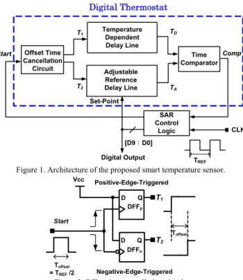
For error reduction, a novel time-domain SAR smart temperature sensor is proposed in this paper with the block diagram shown in Figure 1 which is evolved from the former time-domain digital thermostat [10]. Two delay lines with similar curvatures of the temperature-to-time transfer curves are utilized to lower the nonlinearity impact on the sensor’s accuracy and the SAR control logic is adopted to fasten the digital output coding according to the temperature under test.
The design consideration and detail circuit of the proposed sensor will be described in section II. The experiment results will be illustrated and discussed in section III. Finally, a conclusion will be given in section IV.
II. MAIN BUILDING BLOCKS
The proposed circuit consists of a offset time cancellation circuit to reduce the offset faced at the lower test temperature bound, a temperature-dependent delay line (TDDL) for temperature sensing to generate a delay TD proportional to the measured temperature, a thermally compensated adjustable reference delay line (ARDL) to generate a delay TA according to the programmed set-point, a time comparator for detecting the time difference between TA and TD, and a 10-bit SAR control logic to provide successive digital set-point programming. With a nominal temperature range of 0~90°C to fully support commercial IC on-chip sensing, an effective resolution finer than 0.1°C is promised. All sub-circuits will be illustrated in detail as follows.
A. Offset Time Cancellation Circuit
The output delay TD of the temperature-dependent delay line at the lower temperature operation bound is usually much larger than zero. It is proven to cause large measurement offset, long conversion time and great power consumption [7]. One possible solution is to insert enough number of reference delay cells at the beginning of the reference delay line to compensate for this offset time [10]. As an expense, more chip area and dissipation power must be consumed. In order to solve the above problem, a simple but practical offset time cancellation circuit composed of only two D-type flip-flops (DFFs) is proposed as shown in Figure 2. At the beginning of each comparison, the pulse Start is fed into the clock inputs of both DFFs. The width of the pulse is designed to be equivalent to the offset time Toffset at the lower temperature operation bound. The flip-flop DFFp is triggered by the positive edge of Start, to generate the step signal T1 which is sent to the TDDL input. Similarly, the negative edge of Start triggers the flip- flop DFFn to yield the step signal T2 for ARDL input. The delay difference between T1 and T2 will be identical to Toffset
for offset compensation. The large chip area occupied by the offset-compensation delay cells can be saved, and the ARDL length can be shortened correspondingly.
B. Adjustable Reference Delay Line
As depicted in Figure 3, the ARDL with a binary-weighted structure suitable for SAR operation is adopted [11]. The delay line consists of multiple delay segments whose delays are scaled with binary weights. The temperature compensation circuit adopted in the former time-domain sensor [7] is utilized likewise to reduce the thermal sensitivity of the ARDL delay cell to make its delay act as a unit reference time. However, the conventional thermal compensation circuit consumes continuous power. Some switches are added to shut down its quiescent currents between measurements to reduce self- heating effect. The 2-to-1 multiplexer in each segment is controlled by the corresponding input bit to include or bypass all unit delay cells of the segment in the signal transmission path of TA whose overall delay is proportional to the ARDL input value.
MUX
TA
T2
D0
Segment 0
20X
MUX
D1
Segment 1
21X
MUX
D2
Segment 2
22X
MUX
D9
Segment 9
29X
Figure 3. Adopted 10-bit ARDL with binary-weighted structure.
Dk
In 2kX Out
1X
1X MUX
Slow path Fast path Dummy
Figure 4. Schematic of the ARDL k-th segment.
Temperature Dependent Delay Line
Adjustable Reference Delay Line
Time Comparator TD
TA
Digital Output
Comp
SAR Control
Logic Offset Time
Cancellation Circuit
T1
T2
[D9:D0]
CLK
TREF
Start
Set-Point
Digital Thermostat
Figure 1. Architecture of the proposed smart temperature sensor.
Q D
Q D
Positive-Edge-Triggered
Negative-Edge-Triggered Toffset
Toffset
= TREF /2
T1
T2
Start
DFFn DFFp
Vcc
Figure 2. Offset time cancellation circuit.
Figure 4 shows the entire schematic of the ARDL kth segment. To balance the input loadings of both fast and slow paths in each segment for reducing the error caused by signal distortion at the input, one dummy delay cell is inserted in the beginning of each path at the expense of slightly increased circuit area and conversion time. The overall ARDL propagation delay TA can be lumped as
1
0
2
N k
A offset MUX k X
k
T T N T − d T
=
= + × +∑ , (1) where TMUX is the multiplexer propagation delay taking the dummy delay cell in each path into account and TX is the unit ARDL cell delay respectively. Due to that a multiplexer is placed in each ARDL segment, some extra delay N×TMUX is included in the transmission path. However, the extra delay imposed on TA can be easily compensated for by adding the same number of 2-to-1 multiplexers in the transmission path of TD as illustrated in Figure 5.
To cut the delay line size and the conversion time in half, the delay cell of the ARDL can be theoretically implemented as a temperature-compensated NOT gate instead of a delay buffer [10]. However, the rise time and fall time of the temperature-compensated NOT gate are not equivalent due to the pull up and pull down currents cannot be kept exactly the same after fabrication. This mismatch between even and odd stages will cause additional errors. Therefore, a thermally compensated buffer (or 2 equivalent NOT gates) is used instead as the unit delay cell in ARDL.
C. Temperature-Dependent Delay Line
The TDDL consists of a temperature sensing delay line and N dummy multiplexers to compensate for the delay offset caused by the multiplexers resident in ARDL, as shown in Figure 5. Since there are only N 2-to-1 dummy multiplexers needed to be inserted in TDDL, the chip area consumed by the dummy devices is substantially decreased from that of one 2N- to-1 dummy multiplexer used in the previous thermostat [10].
The temperature sensing delay line is simply composed of even number of NOT gates which are not thermally compensated. The higher the operation temperature is, the longer the propagation delay of NOT gate becomes [7]. Thus, the delay line composed of NOT gates can act as a time- domain PTAT (proportional to absolute temperature) circuit which owns much simpler structure than the conventional voltage-domain ones. The timing relationship between both delay lines is explicitly depicted in the timing diagram of Figure 6. The adjustable range of TA is designed to fully cover the variation of TD for 0~90°C temperature range.
D. Time Comparator and SAR Control Logic
The time comparator only needs to determine whether TA
leads or lags TD. A simple DFF is good enough to be the time comparator by sampling TD with the rise edge of TA. The comparator output Comp is fed into the SAR control logic to determine whether the current SAR bit will be preserved (TA <
TD) or cleared (TA > TD). As an example, the operation of the proposed time-domain sensor with 4 input bits is shown in Figure 7. The thermally sensitive delay TD of the TDDL is fixed for a given temperature. On the contrary, the reference delay TA with much less temperature sensitivity is varied by adjusting the effective length of ARDL according to the set- point value. The SAR algorithm is utilized to speed up the adjustment of TA to approximate TD. For simplicity, the delay faced by TD, TA at the lower temperature bound is denoted as TBASE which equals Toffset+N×TMUX and the maximum adjustable range of TA is represented as TMAX which equals 2N×TX. For a given test temperature, TD is fixed and TA is adjusted successively to approximate TD. The final difference between TA and TD will be less than the unit reference delay TX.
The time comparison error is mainly caused by the dead zone, or sampling window, of DFF. Fortunately, the signals can be easily stretched or amplified along the time axis since there is no hard limit similar to the supply voltage or full-scale voltage of the voltage-domain sensors imposed on the time- domain ones. The unit reference delay TX is designed to be much larger than the DFF dead zone to make the corresponding time error less than 1 LSB. Thus, the impact of dead zone can be reduced straightforwardly by increasing the
MUX
N stages Temperature Sensing
Delay Line Dummy MUXes
MUX
TD
T1
1X 1X
1X 1X
Figure 5. Temperature dependent delay
TD
0° 90°(C)
TBASE
N×TMUX
Toffset
T2
[D9:D0]= 0 1 2 1023
TA
………
…………
Start T1
Figure 6. Timing diagram of the proposed sensor.
TA
TD Delay
TMAX+TBASE
1 2 3 4
Conversion Steps Step 0
(1000) Step 3
(1101) Step 1
(1100) Step 2 (1110) 3/4TMAX+TBASE
1/2TMAX+TBASE
1/4TMAX+TBASE
0 TBASE
Result (1100)
Figure 7 Exemplified operation of the 4-bit time-domain SAR sensor.
number of SAR bits. With 10 SAR bits and a practical temperature range of -2~92°C to cover the possible process variations, the maximum error contributed by the dead zone is less than 0.1°C.
III. EXPERIMENTAL RESULTS
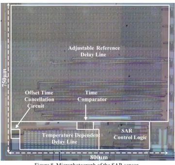
The proposed SAR smart temperature sensor was fabricated in a TSMC standard 0.35-μm 2P4M CMOS digital process. The chip area is 0.75mm×0.8mm as shown in Figure 8. The test input signal was issued by the FPGA control board and the digital output codes were collected by a logic analyzer.
To figure out the performance of the proposed circuit, the measurement of the SAR sensor was done in 5°C steps over 0°C~90°C temperature range in a programmable temperature and humidity chamber MHU-408LRBDA. With the excellent linearity achieved by making TDDL and ARDL have similar temperature-to-time curvatures, the measurement errors are - 0.25~+0.35°C only for total 23 test chips after two point calibration as depicted in Figure 9. Compared with the former time-domain version [8], a four-fold improvement in accuracy is achieved. To reveal the effect of the process variation on the proposed circuit, all the effective resolutions of the test chips are calculated to be within 0.0908~0.0927°C/LSB. The chip- to-chip resolution mismatch is merely ±0.9% which is fairly low for most applications. The power consumption is 36.7µW at 2 samples/s.
IV. CONCULSION
A time-domain SAR smart temperature sensor was proposed in this paper. To reduce the chip size tremendously for portable or low cost applications, a simple offset cancellation circuit was explored to replace a large number of thermal-compensated delay cells for alleviating the large measurement offset faced at the lower temperature bound. The chip area of the 10-bit sensor is 0.6 mm2. The measurement error is within -0.25~+0.35°C over 0°C~90°C which covers
the full temperature operation range of commercial ICs. For total 23 test chips, the chip-to-chip resolution mismatch is merely ±0.9% which demonstrates the good immunity of the proposed sensor to process variations.
ACKNOWLEDGMENT
The authors would like to express their deep appreciation to National Chip Implementation Center (CIC) for the help of chip fabrication.
REFERENCES
[1] P. Krummenacher and H. Oguey, “Smart temperature sensor in CMOS technology”, Sensors and Actuators A: Physical, vol. 22, issue 1-3, pp.636 - 638, June 1990.
[2] R. A. Bianchi, F. Vinci Dos Santos, J. M. Karam, B. Courtois, F.
Pressecq, and S. Sifflet, “CMOS compatible temperature sensor based on the lateral bipolar transistor for very wide temperature range application,” Sensors, Actuators: A. Physical, vol. 71, issue 1-2, pp. 3–
9, Nov. 1998.
[3] G. Wang, and G. C. M. Meijer, “The Temperature Characteristics of Bipolar Transistors Fabricated in CMOS Technology,” Sensors and Actuators A: Physical, vol. 87, issue 1-2, pp. 81-89, Dec. 2000 [4] A. Bakker and J. H. Huijsing, “Micropower CMOS temperature sensor
with digital output,” IEEE J. Solid-State Circuits, vol. 31, pp.933-937, July 1996.
[5] M. Tuthill, “A Switched-Current, Switched- Capacitor Temperature Sensor in 0.6-um CMOS,” IEEE J. Solid-State Circuits, vol. 33, pp.
1117-1122, July 1998.
[6] M. A. P. Pertijs, A. Niederkorn, M. Xu, B. McKillop, A. Bakker, and J.
H. Huijsing, “A CMOS Smart Temperature Sensor with a 3σ Inaccuracy of ±0.1°C from –55°C to 125°C,” IEEE J. Solid-State Circuits, vol. 40, pp. 2805-2815, Dec. 2005.
[7] P. Chen, C.-C. Chen, W.-F. Lu and C.-C. Tsai, “A Time-to-Digital- Converter-Based CMOS Smart Temperature Sensor,” IEEE J. Solid- State Circuits, vol. 40, no. 8, pp. 1642-1648, Aug. 2005.
[8] P. Chen, M.-C. Shie, Z.-Y. Zheng, Z.-F. Zheng and C.-Y. Chu, “A Fully Digital Time Domain Smart Temperature Sensor Realized with 140 FPGA Logic Elements”, IEEE Transactions on Circuits and Systems I, vol. 54, pp. 2661-2668, Dec 2007.
[9] M. A. P. Pertijs, A. Bakker, and J. H. Huijsing, “A high-accuracy temperature sensor with second-order curvature correction and digital bus interface,” in Proc. ISCAS, pp. 368–371, May 2001.
[10] P. Chen, C.-C. Chen, T.-K. Chen, and S.-W. Chen, “A Time-Domain Mixed-Mode Temperature Sensor with Digital Set-Point Programming,” in Proc. IEEE CICC, pp. 821-824, Sept. 2006.
[11] A. Syed, E. Ahmed, D. Maksimovic, and E. Alarcon, “Digital Pulse Width Modulator Architectures,” in Proc. 35th Annual IEEE Power Electronics Specialirls Conference, pp. 4689-4695, June 2004.
[12] T. A. Demassa, and Z. Ciccone, “ Digital Integrated Circuits,” John Wiley & Sons, Inc., 1996.
800µm
750µm
Temperature Dependent Delay Line
Adjustable Reference Delay Line
SAR Control Logic Offset Time
Cancellation Circuit
Time Comparator
Figure 8. Microphotograph of the SAR sensor.
0 10 20 30 40 50 60 70 80 90
-0.2 -0.1 0 0.1 0.2 0.3
Temperature(℃)
Error()℃
Figure 9. Architecture of the proposed smart temperature sensor.