Low Schottky barrier to etched p-GaN using regrown AlInGaN and InGaN contact layer
Kuang-Po Hsueh and Yue-Ming Hsina兲
Department of Electrical Engineering, National Central University, Chung-Li 32054, Taiwan, Republic of China
Jinn-Kong Sheu
Institute of Electro-Optical Science and Engineering, National Cheng Kung University, Tainan 70101, Taiwan, Republic of China
共Received 2 May 2005; accepted 13 December 2005; published online 25 January 2006兲
The p-type AlInGaN and InGaN contact layers were regrown on the etched p-GaN to study the Ni/ Au contact current-voltage共I-V兲 characteristics. The thickness of the contact layer was 100 nm and regrown by metalorganic chemical vapor deposition. By using the regrown contact layer on etched p-GaN, Schottky barrier height共SBH兲 from the I-V characterization was reduced. The SBH of 0.65 eV from the contact to the etched p-GaN was reduced to 0.56 eV and 0.58 eV, respectively, after the AlInGaN and InGaN contact layers were formed. In addition to the I-V characterization of Ni/ Au contacts, surface morphology and x-ray analysis were studied. © 2006 American Institute of Physics.关DOI:10.1063/1.2164527兴
GaN material is important to high-power electronics due to its wide band gap characteristics. Base on the success in the optical devices,1–3 high electron mobility transistors 共HEMTs兲 and heterojunction bipolar transistors 共HBTs兲 for power applications have been under extensive development.4–7 However, it is difficult to obtain good Ohmic contact to p-GaN, especially in the GaN-based HBT process. The major reasons are the low activation rate of acceptors in the base and the damage from dry etching. It has been shown that the roughness and the contamination on the p-GaN surface increased after the dry etching.8–11
Several methods have been utilized to improve the dam- age on etched p-GaN such as replacing the argon by nitrogen in the plasma chemistry,12,13 lowering the plasma power,14 and forming the regrown p-InGaN on the etched p-InGaN.15 In this work we present the effect of Cl2/ Ar dry etching on p-GaN combined with the regrowth of AlInGaN or InGaN as the contact layer. The purpose of the regrown layer was to reduce the dry etching damage and increase the surface dop- ing. Since the electrical property of p-type GaN contact, such as Schottky barrier height共SBH兲, is important for the perfor- mance improvement of devices.16 The Schottky barrier heights共SBHs兲 from I-V characterization for Ni/Au metalli- zation on as-grown, etched, and regrown surfaces were cal- culated to investigate the effect of the regrown contact layer on the etched p-GaN. The surface roughness and x-ray dif- fraction共XRD兲 were also characterized to study the regrown layers.
All p-GaN materials used in this study were grown by metalorganic chemical vapor deposition 共MOCVD兲 on c-face sapphire substrates. Source materials were triethylgal- lium and NH3with H2as a carrier gas for GaN growth. The p-type dopant source was bis-cyclopentadienylmagnesium.
The growth temperature was 1000 ° C. An undoped GaN
buffer layer with a thickness of 2m was grown first, fol- lowed by the growth of 1 m thick p-type GaN doped with Mg. The activation annealing was carried out at 750 ° C for 20 min in the N2 ambient. A sheet resistivity of 3.5
⫻104⍀/䊐 was measured from room temperature Hall mea- surements. The corresponding bulk carrier concentration of
⬃1.9⫻1017cm−3and a mobility of 9.2 cm2V−1s−1were ob- tained. Prior to Cl2/ Ar reactive ions etching 共RIE兲, all samples were ultrasonically degreased with acetone and iso- propyl alcohol for 10 min and then rinsed with de-ionized 共DI兲 water. The dry etching effect of p-GaN using the RIE mode of a high-density plasma system 共Unaxis Nextral 860L兲 was investigated by the Cl2/ Ar mixture gas. The etch- ing conditions were Cl2/ Ar gas flow rates of 150/ 10 sccm, chamber pressure of 20 mTorr, and the rf power of 50 W.
The total etch depth was 200 nm with the etching rate of 13 nm/ min.
After 200 nm GaN etching, Mg-doped AlInGaN or InGaN was regrown by MOCVD on the etched GaN surface as the contact layer. Source materials were triethylgallium, trimethylindium, and NH3 with nitrogen as a carrier gas for InGaN growth. The regrowth temperature was 800 ° C.
Source materials were triethylgallium, trimethylindium, tri- methylaluminum, and NH3 with H2 as a carrier gas for Al- InGaN growth. The regrowth temperature was 900 ° C. The thickness of the regrown contact layer was 100 nm calcu- lated from the in situ reflectance monitoring during growth.
After the regrowth, the magnesium activation annealing was carried out at 750 ° C for 20 min in N2 ambient. The sheet resistivities of 9.0⫻104 and 1.8⫻105 ⍀/square were mea- sured from AlInGaN / GaN and InGaN / GaN materials by room temperature Hall measurements, respectively.
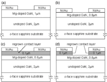
Figure 1 shows the schematic structures with and with- out regrown contact layers for the I-V characterization. All samples with and without regrown contact layers were pat- terned by the standard photolithographic technique. As
a兲Electronic mail: [email protected]
JOURNAL OF APPLIED PHYSICS 99, 026106共2006兲
0021-8979/2006/99共2兲/026106/3/$23.00 99, 026106-1 © 2006 American Institute of Physics
Downloaded 22 Oct 2009 to 140.116.208.44. Redistribution subject to AIP license or copyright; see http://jap.aip.org/jap/copyright.jsp
shown in Fig. 1共d兲, the regrown contact layer between con- tact pads was etched away by dry etching. Prior to metal deposition, hydrofluoric acid was used to remove the native oxide layer on the surface. The Ni共20 nm兲/Au共20 nm兲 con- tact patterns were deposited on all samples by electron beam evaporation and liftoff. The Ni/ Au contact was then an- nealed in an O2-containing ambient at 500 ° C for 5 min. The metal contact size was 100m⫻100m. The spacing be- tween contact pads was 20m. I-V data were measured on those Ni/ Au contact pads using parameter analyzer 共HP4156C兲.
The thickness of the regrown layers was examined by scanning electron microscopy 共SEM兲 and confirmed to be approximately 100 nm. Figure 2 shows the SEM images of the regrown surfaces. The images show the significant differ- ences between the regrown AlInGaN and InGaN surfaces.
Figure 2共a兲 shows the alumina droplet that is due to the Al content in AlInGaN material. The roughness shown in Fig.
2共b兲 is related with the high indium composition. The surface morphologies of all samples were characterized by atomic force microscopy共AFM兲 on a 10⫻10m2surface to obtain the surface root-mean-square 共rms兲 roughness. The average rms roughness of the regrown AlInGaN surface and InGaN surface were 5.01 nm and 6.46 nm, respectively. The surface roughness from AFM confirmed the SEM observation that the AlInGaN contact layer showed less surface roughness than InGaN. Figure 3 shows the x-ray diffraction 共XRD兲 patterns on samples with and without regrown layers by con-
ducting 2-scans around 0002 reflection. All three patterns demonstrate the strong GaN peaks with secondary peaks for regrown layers. The regrown AlInGaN material demonstrates a better lattice match to the bulk p-GaN than the regrown InGaN material. The indium composition of the regrown In- GaN from the XRD calculation is 0.22. A high indium con- tent was intended to obtain high hole concentration.17,18 However, the high indium composition and thus large lattice mismatch causes the high surface roughness, as observed in Fig. 2. Figure 4 shows the measured I-V characteristics from Ni/ Au contact pads for the different material systems, as described in Fig. 1. The metal contact on the as-grown p-GaN surface demonstrates excellent Ohmic contact char- acteristics. The metal contact on the etched p-GaN surface shows the significant Schottky barrier. But a lower Schottky barrier is observed from the contacts to the etched p-GaN using regrown AlInGaN or InGaN contact layers. In order to determine the effective SBH of the Ni/ Au contacts, the I-V method was employed. The I-V relation is given by19
FIG. 1. Ni/ Au contact pads on共a兲 the as-grown p-GaN surface, 共b兲 the etched p-GaN surface,共c兲 the regrown contact layer, and 共d兲 the patterned regrown contact layer.
FIG. 2. The SEM images of共a兲 the regrown AlInGaN surface morphology, and共b兲 the regrown InGaN surface morphology.
FIG. 3. The XRD patterns of three different material systems including bulk p-GaN, regrown AlInGaN on bulk p-GaN and regrown InGaN on bulk p-GaN.
FIG. 4. Measured I-V characteristics for Au/ Ni contacts to different materials.
026106-2 Hsueh, Hsin, and Sheu J. Appl. Phys. 99, 026106共2006兲
Downloaded 22 Oct 2009 to 140.116.208.44. Redistribution subject to AIP license or copyright; see http://jap.aip.org/jap/copyright.jsp
J = A**T2exp冉−⌽bkT冊冋exp冉nkTqV冊− 1册, 共1兲
where A**, the effective Richardson constant, is 96.1 A cm−2K−2for p-GaN; J is the current density; T is the measurement temperature in Kelvin;⌽b is the SBH; n is the ideality factor; and k is Boltzmann’s constant. From Eq.共1兲, the extracted SBH was 0.40 eV and 0.65 eV for the contacts to the as-grown and the etched p-GaN, respectively. The cal- culated 0.40 eV from the as-grown p-GaN is similar to the published value of 0.47 eV.19The increased 0.25 eV showed the significant effect after dry etching. The extracted SBH from Ni/ Au contact pads on the bulk contact layers was 0.45 eV for AlInGaN and 0.44 V for InGaN materials, re- spectively. The SBH of 0.65 eV from the contact to the etched p-GaN was reduced to 0.56 eV and 0.58 eV, respec- tively, after the AlInGaN and InGaN contact layers were formed.
Two p-type materials 共AlInGaN and InGaN兲 were re- grown on etched p-GaN to study the characteristics of the contact layers. In addition to the effects of the I-V character- istics of Ni/ Au contacts, surface morphology and x-ray analysis were studied. By using the regrown contact layers on etched p-GaN, reduced SBHs contacts were obtained.
The SBHs of the samples with the AlInGaN and InGaN con- tact layer were reduced to 0.56 eV and 0.58 eV, respectively.
ACKNOWLEDGMENT
The authors would like to thank the National Science Council of the Republic of China, Taiwan for financially sup- porting this research under Contract No. NSC 93-2215-E- 008-019.
1S. Nakamura, M. Senoh, N. Iwasa, and S. Nagahama, Jpn. J. Appl. Phys., Part 2 34, L797共1995兲.
2S. Nakamura, M. Senoh, N. Iwasa, T. Yamada, T. Matsushita, H. Kiyoku, and Y. Sugimoto, Jpn. J. Appl. Phys., Part 2 35, L217共1996兲.
3M. Asif Khan, J. N. Kuznia, D. T. Olson, J. M. Van Hove, M. Blasingame, and L. F. Reitz, Appl. Phys. Lett. 60, 2917共1992兲.
4M. Asif Khan, A. R. Bhattarai, J. N. Kuznia, and D. T. Olson, Appl. Phys.
Lett. 63, 1214共1993兲.
5T. Makimoto, Y. Yamauchi, and K. Kumakura, Appl. Phys. Lett. 84, 1964 共2004兲.
6F. Ren, J. Han, R. Hickman, J. M. Van Hove, P. P. Chow, J. J. Klaassen, J.
R. LaRoche, K. B. Jung, H. Cho, X. A. Cao, S. M. Donovan, R. F. Kopf, R. G. Wilson, A. G. Baca, R. J. Shul, L. Zhang, C. G. Willison, C. R.
Abernathy, and S. J. Pearton, Solid-State Electron. 44, 239共2000兲.
7L. S. McCarthy, I. P. Smorchkova, H. Xing, P. Kozodoy, P. Fini, J. Limb, D. L. Pulfrey, J. S. Speck, M. J. W. Rodwell, S. P. DenBaars, and U. K.
Mishra, IEEE Trans. Electron Devices 48, 543共2001兲.
8H. Ishikawa, S. Kobayashi, Y. Koide, S. Yamasaki, S. Nagai, J. Umezaki, M. Koike, and M. Murakami, J. Appl. Phys. 81, 1315共1997兲.
9J.-L. Lee, M. Weber, J. K. Kim, J. W. Lee, Y. J. Park, T. Kim, and K.
Lynn, Appl. Phys. Lett. 74, 2289共1999兲.
10C. B. Vartuli, S. J. Pearton, J. W. Lee, J. Hong, J. D. MacKenzie, C. R.
Abernathy, and R. J. Shul, Appl. Phys. Lett. 69, 1426共1996兲.
11C.-C. Kao, H. W. Huang, J. Y. Tsai, C. C. Yu, C. F. Lin, H. C. Kuo, and S.
C. Wang, Mater. Sci. Eng., B B107, 283共2004兲.
12J. M. Lee, K. M. Chang, S. W. Kim, C. Huh, I. H. Lee, and S. J. Park, J.
Appl. Phys. 87, 7667共2000兲.
13Z. Mouffak, A. Bensaoula, and L. Trombetta, J. Appl. Phys. 95, 727 共2004兲.
14J. K. Sheu, Y. K. Su, G. C. Chi, M. J. Jou, C. C. Liu, C. M. Chang, and W.
C. Hung, J. Appl. Phys. 85, 1970共1999兲.
15T. Makimoto, K. Kumakura, and N. Kobayashi, Jpn. J. Appl. Phys., Part 1 43, 1922共2004兲.
16T. Mori, T. Kozawa, T. Ohwaki, Y. Taga, S. Nagai, S. Yamasaki, S. Asami, N. Shibata, and M. Koike, Appl. Phys. Lett. 69, 3537共1996兲.
17K. Kumakura, T. Makimoto, and N. Kobayashi, J. Cryst. Growth 221, 267 共2000兲.
18T. Gessmann, Y. L. Li, E. L. Waldron, J. W. Graff, E. F. Schubert, and J.
K. Sheu, Appl. Phys. Lett. 80, 986共2002兲.
19S. J. Pearton, F. Ren, A. P. Zhang, and K. P. Lee, Mater. Sci. Eng., R. R30, 55共2000兲.
026106-3 Hsueh, Hsin, and Sheu J. Appl. Phys. 99, 026106共2006兲
Downloaded 22 Oct 2009 to 140.116.208.44. Redistribution subject to AIP license or copyright; see http://jap.aip.org/jap/copyright.jsp