Novel Hybrid Control Technique with Constant On/Off Time Control for DC/DC Converter to Reduce
the Switching Losses
Chia-An Yeh and Yen-Shin Lai, Senior Member, IEEE,
Center for Power Electronics Technology, National Taipei University of Technology 1, Sec. 3, Chung-Hsiao E. Rd., Taipei, Taiwan
Abstract-- It has been shown that the resolution of DPWM can be dramatically increased by either constant on-time modulation or constant off-time modulation as compared to that for constant frequency modulation. However, the switching frequency increases dramatically for constant on/off-time modulation method under heavy/light load conditions. The objective of this paper is to propose a hybrid control technique with constant on/off-time control for DC/DC converter in order to reduce the switching frequency and switching losses. It will be shown that the proposed technique can significantly reduce the switching frequency of converter and thereby improving the efficiency up to 2%.
Keywords-hybrid control; constant on-time control; constant off time control
I. INTRODUCTION
It is well known that digital power control provides less component aging, programmable platform, and robustness to noise. Furthermore, it is also with the advantages of short time-to-market and easy implementation of multi-loop control.
Therefore, digital power control has been widely investigated recently [1-6]. However, the limit cycle issue caused by the resolution of Digital Pulse-Width Modulator (DPWM) and quantization error of A/D converter in digital control application [7] results in the oscillation of output voltage of converter even under steady state condition. Several techniques have been proposed to increase the effective modulation resolution [7-11]. It has been shown in [11] that the resolution of DPWM can be dramatically increased by either constant on-time modulation or constant off-time modulation as compared to that for constant frequency modulation.
Constant on/off-time control has been discussed in several applications [12]-[15]. However, as shown in Fig. 1, under constant on-time operation, the switching frequency and the accompanied switching losses significantly increase as the load increases. The increase of switching frequency is contributed by both load and the non-ideal characteristics of components, including turn-on resistor of power devices and resistor of passive components. This paper proposes a novel digital pulse-width modulation technique in order to reduce switching frequency and switching losses for constant on-time
and off-time modulation. The basic idea of the proposed technique is to control the converter using constant on-time modulation under light load condition in order to reduce the switching frequency. In contrast, under heavy load condition, the converter is operated in constant off-time to reduce the switching frequency as shown in Fig.1.
This paper is organized as follows. The proposed hybrid modulation and switching control method is revealed in section II. Modeling and controller design of converter using the proposed hybrid modulation technique will be discussed in section III. Experimental results are presented in section IV.
Fig.1 Switching frequency vs. output load II. NOVEL HYBRID CONTROL TECHNIQUE A. Proposed hybrid control technique
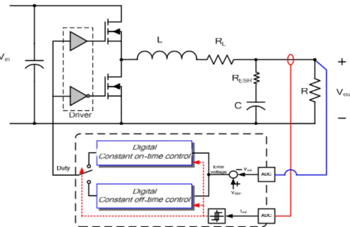
Fig.2 shows the block diagram of buck converter with proposed modulation method. In this block diagram, constant on-time control and constant off-time control are included in digital control unit as shown in Fig.3. When the switch is connected to ”0”, converter will be operated by constant on-time controller. When the switch is connected to ”1”, converter will be operated by constant off-time controller. The status of switch, “1” or “0”, is determined by output current such that the switching frequency keeps in a lower manner under any load condition. The threshold value of load current for the change of switching status will be determined by the upper bound of switching frequency. The relationship between switching frequency and load current will be discussed in Sub-section C.
Fig.2 Buck converter with proposed modulation method
As shown in Fig. 3, when error between reference and the output voltage is positive (output is smaller than its reference), increase of duty is required. For constant on-time control, off-time should be reduced to reflect this request of duty increase. However, for constant off-time control, on-time should be increased in order to increase the duty under this circumstance.
In contrast, when error between reference and the output voltage is negative (output is greater than its reference), off-time for constant on-time control should be increased while on-time for constant off-time control should be decreased. Therefore, as shown in Fig. 3, an 180-degree phase shifter of error voltage (error voltage is multiplied by -1) is required between constant on-time and constant off-time control in order to reflect these facts.
Moreover, in order to give a smooth transition, in the vicinity of transition point, two controllers are in operation simultaneously while one of the outputs is used for control.
Fig.3 Block diagram of proposed control method B. Modulation method for the proposed control method
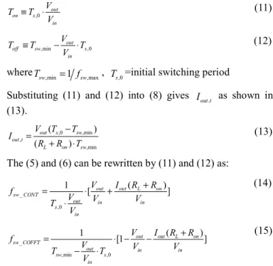
It is well known that the carrier is with fixed peak while the modulating signal is determined by the controller. For constant on-time and constant off-time control, the peak value is not fixed in order to retain constant on-time or constant off-time. Fig. 4 shows modulation process for constant on-time and constant off-time modulation control. As shown in Fig. 4 (A) for constant on-time modulation control, on-time
is constant and off-time is variable and determined by the peak value of carrier. The duty ratio of constant on-time modulation is derived as:
on on off
d T
T t
= + (1)
According to Fig. 4(B) for constant off-time modulation control, the duty ratio of constant off-time modulation is determined by:
on
on off
d t
t T
= + (2)
Vcmp
toff
Ton Toff
(A) Constant on-time modulation, d T= on (Ton+toff)
Vcmp
Ton
Toff ton
(B) Constant off-time modulation, d t= on (ton+Toff) Fig. 4 Modulation process
C. Analysis of switching frequency
In this section, switching frequency for constant on-time modulation and constant off-time modulation are analyzed.
Fig. 2 illustrates the system configuration of the proposed technique using a buck converter as an example. Considering the non-ideal characteristics of power devices and passive component, the duty of converter varies with load [16]. The non-ideal characteristics of power devices and passive component inductor include turn-on resistor of MOSFET, Ron, and DC resistor of inductor, RL. As shown in Fig.2, the duty ratio of buck converter can be derived and shown as:
( )
out L L on
in in
V I R R
D V V
= + + (3)
Under steady state, the average inductor current is equal to output current. Then (3) can be rewritten as:
( )
out out L on
in in
V I R R
D V V
= + + (4)
When converter is operated in constant on-time control, T on is constant andt is variable. The switching frequency of off constant on-time control can be shown by:
_
( )
1 1 [ out out L on ]
sw CONT
on off on in in
V I R R
f T t T V V
= = ⋅ + +
+ (5)
As converter is operated in constant off-time modulation, t is variable andon T is constant. The switching frequency off of constant off-time modulation can be determined by:
_
( )
1 [1 out out L on ]
sw COFFT
off in in
V I R R
f T V V
= ⋅ − − + (6)
By (5) and (6), it is obviously that the switching frequency variation is contributed by the non-ideal characteristics of power devices and passive component inductor which include turn-on resistor of MOSFET, Ron, and DC resistor of inductor, RL. As the load increases, the switching frequency increases for constant on-time modulation. In contrast, the switching frequency decreases for constant off-time modulation.
For the converter with a given maximum switching frequency the transition point indicated by the related load current, Iout t, , can be derived by (5) and (6). When fsw off_ equals to fsw on_ , the output current is defined asIout t, . And by (5) and (6), the following equation can be derived:
,( ) ,( )
1 [ out out t L on ] 1 [1 out out t L on ]
on in in off in in
I R R I R R
V V
T V V T V V
+ +
⋅ + = ⋅ − − (7)
The (7) can be rewritten as:
, [ (1 )]
( ) (1 )
on out on in
out t
off in off on
L on
off
T V T V
I T V T R R T
T
= − ⋅ + ⋅
+ ⋅ +
(8)
For constant on-time modulation control, the maximum switching frequency, fsw,max, can be derived by substituting (8) into (5) to give:
,max
( )
1 [ ]
out
on off on
out in
sw
on in off on
T V T T
V V
f T V T T
− ⋅ +
= ⋅ +
+ (9)
For constant off-time modulation control, the maximum switching frequency, fsw,max, can be derived by substituting (8) into (6) to give:
,max
( )
1 [1 ]
out
on off on
out in
sw
off in off on
T V T T
V V
f T V T T
− ⋅ +
= ⋅ − −
+ (10)
Moreover, T and on T are defined as follows: off
,0 out
on s
in
T T V
≡ ⋅V (11)
,min out ,0
off sw s
in
T T V T
≡ −V ⋅ (12)
whereTsw,min=1 fsw,max, T =initial switching periods,0
Substituting (11) and (12) into (8) gives Iout t. as shown in (13).
,0 ,min
,
,min
( )
( )
out s sw
out t
L on sw
V T T
I R R T
= −
+ ⋅ (13)
The (5) and (6) can be rewritten by (11) and (12) as:
_
,0
( )
1 [ out out L on ]
sw CONT
out in in
s in
V I R R
f T V V V
V
= ⋅ + +
⋅
(14)
_
,min ,0
( )
1 [1 out out L on ]
sw COFFT
out in in
sw s
in
V I R R
f T V T V V
V
= ⋅ − − +
− ⋅
(15)
According to (13)-(15), the switching frequency of the proposed modulation method can be obtained as:
,0 ,min
,0 ,min
_
,0 ,min
,min ,0 ,min
( )
( )
1 [ ] 0
( )
( )
( )
1 [1 ]
( )
out s sw out out L on
out
out in in L on sw
s in sw proposed
out s sw out out L on
out in in L on sw
sw s
in
V T T V I R R
V V V I R R T
T V
f V I R R V T T
V V V R R T
T T
V
+ −
⋅ + ≤ <
⋅ + ⋅
= ⋅ − − + − ≤
− ⋅ + ⋅ out out,max
I I
⎧⎪
⎪⎪
⎨⎪ <
⎪⎪
⎩
(16)
As shown in (13), the variation of Iout t. is contributed by turn-on resistor of MOSFET, Ron, and DC resistor of inductor, RL. Fig. 5 illustrates the relationship between load current and frequency in two kinds of RL for proposed control method.
Some of the remarks can be derived from Fig. 5.
For the same maximum converter switching frequency limitation, as RL decreases, the transition point will move toward greater current.
The constant on-time modulation control range is extended, while decreasing the constant off-time modulation control range as RL deceases.
Fig. 5 The relationship between load current and frequency in three kinds of RL
III. CONTROLLER DESIGN A. Converter Modeling
In order to design the controller, the converter model is derived first. Both DC resistor of inductor and ESR of capacitor are taken into account for more accurate modeling results. The transfer function between output voltage current and duty in s-domain, G svd( ), can be obtained by average state space method [16] as:
2
ˆ ( ) ( 1)
( ) ˆ( ) [ ( ) ]
out in ESR
vd
L on ESR L on
v s V R sCR
G s d s RLCs CR R R L CR R s R R R
= ≅ +
+ + + + + + + (17)
The related equation of (17) in z-domain can be derived by Tustin approximation [17] as:
2
2 2 2
2
[(2 ) 2 2 ]
ˆ ( )
( ) ˆ( ) [4 2( ) ] (2 8) (4 2( ) )
in s
ESR s s s ESR
out vd
L on s s s L on s s
V T CR T z Tz T CR
v z LC
G z d z R R T T z T z R R T T
L LC LC L LC
+ + + −
= ≅
+ +
+ + + − + − +
(18)
where
vd( )
G z : Transfer function between output voltage and duty in z-domain
B. Modeling of modulator
Fig. 6 shows modulation process and perturbation for constant on-time and constant off-time modulation control. As shown in Fig. 6 (A) for constant on-time modulation control, the perturbation indicates by the variable components of carrier which marked by dashed line. The response to the perturbation is indicated by (19).
ˆ
off off ˆoff
d D d
t T t
= +
= + (19)
Substituting (19) into (1) gives the DC and AC terms as shown in (20) and (21), respectively. Note that the non-linear terms are neglected.
(Ton+toff)⋅ =D Ton (20)
_
ˆ -
ˆoff on off m COFFT
d D
t T T F
⎛ ⎞
≅ ⎜⎜⎝ + ⎟⎟⎠=
(21)
According to Fig. 6(B) for constant off-time modulation control, DC and AC terms in response to the perturbation can be derived as shown in (22) and (23), respectively.
(ton+Toff) (1⋅ −D)=Toff (22)
_
ˆ 1
ˆon on off m CONT
d D
t T T F
≅ − =
+ (23)
Vcmp
toff
Ton Toff
ˆoff
t
(A) Constant on-time modulation,D T= on (Ton+Toff)
,
ˆ on ( on off ˆoff) D d T+ = T +T +t
Vcmp
Ton
Toff ton ˆon t
(B) Constant off-time modulation, ( )
on on off
D T= T +T
,
ˆ (ˆon on) (ˆon on off) D d+ =t +T t + +T T
Fig. 6 Modulation process and perturbation C. Controller design
The plant diagram can be further simplified as shown in Fig.7.
The loop-gain transfer function of constant on-time modulation excluding voltage controller can be derived as:
_
2
2 2 2
2
T(z)=H ( )
- [(2 ) 2 2 ]
2( ) 2 2( )
[4 ] ( 8) (4 )
vd m off
in s
ESR s s s ESR
on off
L on s s s L on s s
G z F
V T
D H CR T z T z T CR
T T LC
R R T T T R R T T
z z
L LC LC L LC
⋅ ⋅
⋅ ⋅ + + + −
= +
+ +
+ + + − + − +
(24)
Substituting the designed circuit parameters shown in Section IV into (24), the loop gain of buck converter under constant on-time modulation is obtained as:
2 2
0.003277 0.001693 0.001583
( ) 1.851 0.8614
z z
T z z z
− − +
= − + (25)
The compensator is designed based upon the well known proportional-integral controller. The related z-domain model of a PI-compensator is:
( ) ( )
2 2
( ) 1
I s I s
p p
CV
K T K T
K z K
C z
z
+ − −
= − (26)
The zero of PI-compensator is placed near the dominant pole of T(z) and the system bandwidth can therefore be determined
by the DC gain of PI-compensator. For the specifications of bandwidth (BW) = 10 kHz (FSW 10) and phase margin (PM)
> 45 degrees, the digital compensator can be derived by this method to give:
,
30.297 30
( ) 1
CV CONT
C z z
z
= − −
− (27)
According to (24)-(27), the designed controller for constant off-time modulation can be obtained as:
,
30.297 30
( ) 1
CV COFFT
C z z
z
= −
− (28)
ˆ ( )o ref v z
v
d zˆ( )ˆon off/ ( )
t z
Fig. 7 z-domain model of constant on/off-time modulation buck converter Table I design specification
constant on-time modulation
constant off-time modulation Controller KP 30.16 KP 30.16
KITs 0.2744 KITs 0.2744
Command, Vcmp 135 270
Bandwidth 11.2 kHz 11.9 kHz
Phase Margin 51.7 deg 51.7 deg
IV. EXPERIMENTAL RESULTS
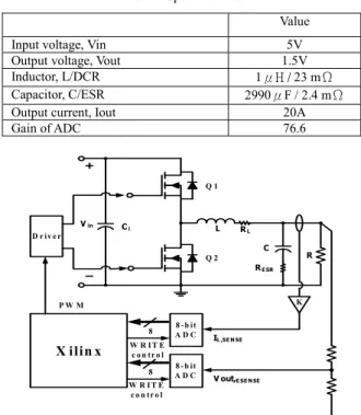
Fig. 8 shows the experimental system which consists of a buck converter with synchronous rectification and an FPGA-based digital controller for proposed hybrid control technique. And the details of converter specifications and components are shown in Table II.
Fig. 9 shows the switching frequency of conventional constant on-time, constant off-time and proposed techniques.
As shown in Fig. 9 (A), the switching frequency for constant on-time control goes up under heavy load condition. The simulation results derived from (14) is confirmed by the experimental results and both agree wit each other. Similar results can be derived for constant off-time control. The exception is the switching frequency becomes lower under light load condition. In contrast, as shown in Fig. 9 (B) for the proposed technique, the switching frequency is within a limited range despite of load changes and the proposed hybrid control technique can significantly reduce the switching frequency and switching losses. Fig. 10 shows the experimental results around the transition point. As shown in Fig. 10, the voltage ripple is less than 38 mV, 2.5% of output voltage under both conditions. Fig. 11 shows the dynamic response to load impact. As shown in Fig. 11, the voltage ripple is less than 106 mV, ±3.53% of output voltage. Fig. 12 shows the measured results of efficiency. As shown in Fig. 12, the efficiency improvement by the proposed technique is up to 2%.
Table II Specifications
Value
Input voltage, Vin 5V
Output voltage, Vout 1.5V
Inductor, L/DCR 1μH / 23 mΩ
Capacitor, C/ESR 2990μF / 2.4 mΩ
Output current, Iout 20A
Gain of ADC 76.6
RL
L C RE SR
R Q 1
Q 2 Ci
Vin
K
X ilin x
8
8 W R I T E c o n tr o l
W R I T E c o n tr o l
V out,E SE N SE
IL ,SE N SE
P W M D r iv e r
8 -b it A D C 8 -b it A D C
Fig. 8 System of the experimental setup
180 190 200 210 220 230 240 250 260 270 280 290 300
0 2 4 6 8 10 12 14 16 18 20
Iout (A)
Fsw (kHz)
Constant on-time (experimental) Constant off-time (experimental) Constant on-time (simulation) Constant off-time(simulation)
(A) constant on/off time, experimental and simulation
Proposed
190 200 210 220 230
0 2 4 6 8 10 12 14 16 18 20
Iout (A)
Fsw (kHz)
Proposed
(B) proposed, experimental Fig. 9 Switching frequency vs. output load
(A) Constant on-time transfer to constant off-time modulation
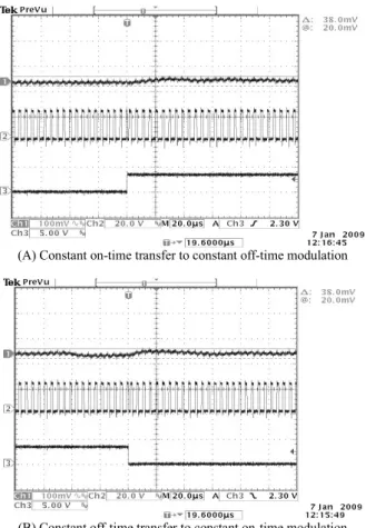
(B) Constant off-time transfer to constant on-time modulation Fig. 10 Experimental results, transition point, Ch 1 = Output voltage, Ch 2 =
High-side modulation signal, Ch 3 = Signal for transition (High = Constant off-time, Low = Constant on-time)
Fig. 11 Experimental results, transient response (5A-15A)
70 72 74 76 78 80 82 84 86 88
2 4 6 8 10 12 14 16 18 20 22
Output current (A)
Efficiency (%)
Constant off-time Constant on-time Proposd
Fig. 12 Experimental results, efficiency
V. CONCLUSION
This paper proposes a new hybrid control technique which provides constant on-time and off-time control. The effective of DPWM resolution is increased as compared to that for conventional constant frequency PWM method. Moreover, the switching frequency is significantly reduced comparing to either constant on-time or constant off-time control.
Experimental results demonstrate the effectiveness of the proposed hybrid control technique and the efficiency improvement is up to 2%.
REFERENCE
[1]. D. Maksimovic,. R. Zane, and R. Erickson, “Impact of digital control in power electronics,” IEEE ISPSD, pp.13 – 22, May, 2004.
[2]. A. V. Peterchev, J. Xiao,and S. R. Sanders ,” Architecture and IC Implementation of a Digital VRM Controller,” IEEE Trans. on Power Electronics, Vol. 18, No. 1, pp.356-364, Jan., 2003.
[3]. Y. S. Lai, C. A. Yeh, Y. T. Chang and K. Y. Lee, ”New self-commissioning digital power converter with peak current mode control and leading edge modulation using low sampling frequency A/D converter,” IEEE IAS, pp.2351-2356, 2007.
[4]. A. G. Perry, G. Feng, ,Y. F. Liu and P. C. Sen, “A design method for PI-like fuzzy logic controllers for dc–dc converter,” IEEE Trans. on Industrial Electronics, Vol. 54, No. 5, pp.2688-2696, Oct., 2007.
[5]. L. Corradini, E. Orietti, P. Mattavelli and S. Saggini, “Digital hysteretic voltage-mode control for dc–dc converters based on asynchronous sampling,” IEEE Trans. on Power Electronics, Vol. 24, Issue 1, pp.201 – 211, Jan., 2009.
[6]. J. Morroni, R. Zane and D. Maksimovic, “Design and implementation of an adaptive tuning system based on desired phase margin for digitally controlled dc–dc converters,” IEEE Trans. on Power Electronics, Vol.
24, Issue 2, pp.559 – 564, Feb., 2009.
[7]. A. V. Peterchev and S. R. Sanders, “Quantization resolution and limit cycling in digitally controlled PWM converters,” IEEE Trans. on Power Electronics, Vol. 18, No. 1, pp.301-308, Jan., 2003.
[8]. Z. Lukic, N. Rahman, and A. Prodic, “Multibit Σ---Δ PWM digital controller IC for dc---dc converters operating at switching frequencies beyond 10 MHz,” IEEE Trans. on Power Electronics, Vol.22, No.5, pp.
35-40, Sep., 2007.
[9]. S. Yi, L. Jian, X. Ming and F.C. Lee, “Novel digital multi-phase duty cycle modulation methods for voltage regulators,” IEEE APEC, pp.1099 – 1105, Feb., 2008.
[10]. L. Peng, Y. Kang, X. Pei and J. Chen, “A novel PWM technique in digital control,” IEEE Trans. on Industrial Electronics, Vol. 54, Issue 1, pp.338 – 346, Feb., 2007.
[11]. J. Li, Y. Qiu, Y. Sun, B. Huang, M. Xu, D. S. Ha, and F. C. Lee, “High resolution digital duty cycle modulation schemes for voltage regulators,” IEEE APEC, pp.871 – 876, Mar. 2007.
[12]. X. Xu and X. Wu, “High dimming ratio LED driver with fast transient boost converter,” IEEE PESC, pp.4192 – 4195, June, 2008.
[13]. T.Y. Yang and J. Y. Lin, “PWM controller having adaptive off-time modulation for power saving,” US patent 66661679, Oct., 2002. System General Inc.
[14]. W. H. Chang, H. S. Nien and C. H. Chen, “A digital boost converter to drive white LEDs,” IEEE APEC, pp.558 – 564, Feb., 2008.
[15]. N. Kong, D. S. Ha, J. Li and F. C. Lee, ”Off-time prediction in digital constant on-time modulation for dc-dc converters,” IEEE ISCAS, pp.3270 – 3273, May, 2008.
[16]. R. W. Erickson, and D. Maksimovic, “Fundamental of Power Electronics, ” 2nd edition, Kluwer Academic Publishers, 2001.
[17]. G. F. Franklin, J. D. Powell, and M. L. Workman, Digital Control of Dynamic Systems, 3rd ed. Reading, MA: Addison Wesley, 1998.