doi:10.6342/NTU201600721
國立臺灣大學電機資訊學院電子工程學研究所 碩士論文
Graduate Institute of Electronics Engineering College of Electrical Engineering and Computer Science
National Taiwan University Master Thesis
利用原子層沉積技術成長氧化層並 製作免轉印上閘極石墨烯及二硫化鉬電晶體 Graphene and MoS2 Transferring-Free Top-Gated Transistors with Dielectric Layers Fabricated by Using the
Atomic Layer Deposition
懷碩 Shuo Hwai
指導教授:吳肇欣 博士 林時彥 博士 Advisor: Chao-Hsin Wu, Ph.D.
Shih-Yen Lin, Ph.D.
中華民國 105 年 6 月 June 2016
doi:10.6342/NTU201600721
I
口試委員審定書
doi:10.6342/NTU201600721
II
Verification letter from the Oral Examination
Committee
doi:10.6342/NTU201600721
III
致謝
碩士兩年生涯在轉瞬間就來到尾聲,本論文得以順利如期完成,全歸功於太 多人的提攜與扶持。感謝我的兩位指導教授:吳肇欣博士及林時彥博士,感謝他 們無時無刻都為我的生涯規劃著想,提供我難能可貴的機會與研究上重要的指導,
在兩年的學習中,能夠一步一步讓自己邁向專業。感謝兩個實驗室所有現役成員 及畢業學長對我的包容與鼓勵,有你們的幫忙,才有辦法關關難過關關過。感謝
IOED 的立成、承翰、Lucas 學長,儘管我後來較少出現在實驗室也沒有幫你們什 麼忙,你們仍然對我有求必應,也感謝俊諺、雲聲學長,雖然相處不多但你們也 給我有用的建言與鼓勵。感謝我的 IOED 同梯:家銘、棋翔、勇霖、尚封、宗翰、
楊旻、貿鍾及開能,真的很慶幸能在 IOED 與你們相遇。感謝 Lin Group 的崇榮、
冠超及璿安學長,包容我的堅持並持續給我最大的幫助。感謝同梯:崑成、宣佑 及翔睿,讓感受第二個家的溫暖。感謝 IOED 所有可愛的學弟學妹,原諒我因為篇 幅無法一一點名,但看到你們讓我更知道要無時無刻得鞭策自己往前進。感謝 Lin
Group 的統威及偉展,無條件支援我。感謝中研院應科中心的謝書宜博士,在實驗 設備上給我最大的照應與協助。感謝我的家人,對我所有的任性要求,給予義無 反顧的支持與鼓勵。感謝我的女朋友,願意陪同我一起成長茁壯。
這些恩情懷碩將永遠銘記在心,沒齒難忘,也必定努力表現不讓大家失望。
懷碩亦會秉持著飲水思源的心,給予所有人最多的幫助,期盼功成名就時,能有 能力回饋國家社會。
doi:10.6342/NTU201600721
IV
摘要
本篇論文著重在於二維材料中石墨烯及二硫化鉬免除轉印製程的上閘極電晶 體的製作,由於氧化層的成長對於上閘極電晶體的特性極為重要,所以我們先最 佳化了以原子層沉積技術成長高介電係數三氧化二鋁於石墨烯的成長參數,接著 將其應用至二硫化鉬上閘極電晶體。此外,本論文也藉由下閘極電晶體開始,最 終製成雙閘極結構的電晶體來探討氧化層對於下閘極電晶體的影響以及比較上閘 極及下閘極電晶體之元件特性差別。
本論文可分為兩大部份,第一部分為免轉印石墨烯上閘極電晶體的製作,首 先藉由不同成長參數的探討找出最佳原子層沉積條件,其中使用最佳條件製得的 上閘極石墨烯電晶體具有 15.4 cm2V-1s-1之電洞遷移率以及 13.6 cm2V-1s-1之電子遷 移率,此外其電流滯後現象少於 2 V 以及擁有在 0 V 之狄拉克點。雙閘極電晶體亦 製作用來比較上閘極與下閘極電晶體的差異,其中我們發現下閘極電晶體在原子
層沉積氧化層後,元件特性大幅提升,電洞遷移率由 660 cm2V-1s-1 提升至 993
cm2V-1s-1而電子遷移率也由 469 cm2V-1s-1 提升至 911 cm2V-1s-1,推測應是肇因於此 氧化層有保護石墨烯免於環境污染的功效,而當雙閘極電晶體的上閘極電極製作 上去後,上及下閘極之元件特性皆變差,推測氧化層因為電子束蒸鍍之熱能而損 壞,以及氧化層中的氧原子藉由熱能與石墨烯形成氧化石墨烯而造成載子遷移率 下降。
第二部分中我們將原子層沉積氧化層於石墨烯上的技術應用至二硫化鉬並且
doi:10.6342/NTU201600721
V
成功製造出上閘極二硫化鉬電晶體,其電子遷移率為 0.13 cm2V-1s-1。在二硫化鉬
薄膜轉印至二氧化矽/矽基板後,二硫化鉬雙閘極電晶體亦被製作用來比較上下閘 極的差異。下閘極電晶體在原子層沉積氧化層後,元件特性大幅提升的現象亦被 觀察到,電子遷移率由 0.0097 cm2V-1s-1提升至 0.045 cm2V-1s-1,接著進行上閘極金 屬蒸鍍製程做成雙閘極電晶體,發現下閘極電晶體的電子遷移率顯著上升,我們 推測乃因鍍金屬時的熱能使得氧化層中的氧原子與二硫化鉬形成導電度較佳的氧 化鉬,因而提升載子遷移律。由載子遷移率可觀察需轉印之上閘極二硫化鉬電晶 體的部分較免轉印的二硫化鉬電晶體低,由此可知免轉印電晶體可免於轉印時造 成的污染而有著更加的電晶體表現。
關鍵字:二維材料、石墨烯、二硫化鉬、場效電晶體、原子層沉積、免轉印
doi:10.6342/NTU201600721
VI
Abstract
In this thesis, we focus on the fabrication of transferring-free top-gated transistors using two-dimensional material: graphene and MoS2 as the channel. The growth of top-gate dielectric is critical in the fabrication process. Therefore, we have optimized the growth conditions of high-k Al2O3 on graphene by the atomic layer deposition technique (ALD). Then, this technique is also applied to top-gated MoS2 transistors.
Additionally, a sequential investigation of dual-gated transistor is carried out to investigate the influence of the top dielectric layer to bottom-gated transistors and the difference between top- and bottom-gated transistors.
This thesis is divided into two parts. The first part is the fabrication of transferring-free graphene transistors. The ALD growth recipe is first investigated. The best recipe is applied to fabricate the transferring-free graphene transistor. The device shows an hole mobility of 15.4 cm2V-1s-1 and electron mobility of 13.6 cm2V-1s-1 with a hysteresis less than 2 V and a Dirac point at 0 V. Then, the dual-gated graphene transistor is made to investigate the difference between top- and bottom-gated transistors. The performance enhancement is found right after the oxide deposition on bottom-gated transistor, showing the increment of hole mobility 660 cm2V-1s-1to 993 cm2V-1s-1from and electron mobility from 469 cm2V-1s-1 to 911 cm2V-1s-1. We believe that the oxide layer acts as a passivation layer to prevent contaminations from the
doi:10.6342/NTU201600721
VII
environment to the graphene channel. However, after the top-gate metal is deposited, the performance of both top- and bottom- gated transistors are degraded. We believe that the heat introduced during e-beam evaporation is responsible for the degradation, which enables graphene to interact with the oxygen atom of the Al2O3 layer and form graphene oxide. In this case, lower conductivity than graphene and thus decreased mobility are observed for the device.
In the second part, the oxide growth technique using ALD is applied to the fabrication of transferring-free top-gated MoS2 transistor. The electron mobility is 0.13 cm2V-1s-1. Dual-gated MoS2 structure is also made to compare top-gated transistor with bottom-gated transistor after the MoS2 film transferred to a SiO2/Si substrate. The performance enhancement of bottom-gated transistor is also observed after the oxide is grown on bottom-gated transistor, the mobility values increase from 0.0097 to 0.045 cm2V-1s-1. However, after the top-gate metal is deposited, the performance of bottom-gated transistors is even further improved. We believe that the heat introduced during the metal deposition is responsible for the improved performance, which would enable MoS2 to interact with the oxygen atom of the Al2O3 layer and form Mo oxides.
The higher conductivity of the material will induce the mobility value enhancement. On the other hand, the top-gated transistor has worse performance comparing with transferring-free top-gated transistor. This difference further proves the advantage of
doi:10.6342/NTU201600721
VIII
transferring-free process that avoids the contamination during transfer process.
Key words – Two-dimensional (2D) material, Graphene, MoS2, Metal-oxide-semiconductor field-effect transistor (MOSFET), transferring-free
doi:10.6342/NTU201600721
IX
Table of Contents
口試委員審定書 ... I Verification letter from the Oral Examination Committee ... II 致謝 ... III 摘要 ... IV Abstract ... VI Table of Contents ... IX List of Figures ... XII List of Tables ... XVII
Chaper 1. Introduction ... 1
1.1. The Upcoming End of Scaling of Silicon MOSFETs ... 1
1.2. Development and Rationale of Two-dimensional Materials ... 3
1.3. Fundamentals of Two-dimensional Materials ... 5
1.3.1. Basics of Graphene ... 5
1.3.2. Basics of MoS2 ... 12
1.4. The Organization of the Thesis ... 15
Chaper 2. Introduction of Experimental Instruments ... 18
2.1. Material Growth and Device Fabrication Instruments ... 18
2.1.1. Low Pressure Chemical Vapor Deposition System (LPCVD) ... 18
doi:10.6342/NTU201600721
X
2.1.2. Transition Metal Deposition System: Radio-frequency (RF) Sputtering
Deposition System ... 22
2.1.3. Transition Metal Sulfurization System: ... 24
2.1.4. Electron beam Evaporation Physical Vapor Deposition System (EBPVD) ... 26
2.1.5. Reactive-Ion Etching (RIE) System ... 28
2.1.6. Atomic Layer Deposition (ALD) System ... 28
2.2. Characterization Instruments ... 32
2.2.1. High Resolution Confocal Raman Spectroscopy ... 32
2.2.2. Transmission Electron Microscope (TEM) ... 34
2.2.3. Atomic Force Microscope (AFM) ... 34
Chaper 3. Top-gated Graphene Transistors Fabricated on Graphene Grown Directly on Sapphire Substrates ... 38
3.1. The Fabrication Procedure of Top-gated Graphene Transistors ... 38
3.1.1. The Growth of Graphene Films Directly on Sapphire Substrates ... 39
3.1.2. The Device Fabrication Procedure of the Graphene Transistors ... 41
3.2. Growth Optimization of Al2O3 Dielectric Layers on Graphene and Device Performances of Top-gated Graphene Transistors ... 41
3.2.1. Device Performances of Top-gated Graphene Transistors ... 55
doi:10.6342/NTU201600721
XI
3.3. Comparison of Graphene Transistors between Top- and Bottom- gated
Structure ... 55
3.4. Conclusions ... 67
Chaper 4. Top-gated MoS2 Transistors Fabricated by Sulfurization of Pre-deposited Mo Films ... 68
4.1. The Fabrication Procedure of Top-gated MoS2 Transistors... 68
4.1.1. The Growth of MoS2 Film by Using Sulfurization of Pre-deposited Mo Films ... 68
4.1.2. The Device Fabrication Procedure of Top-gated MoS2 Transistors ... 71
4.2. The Device Performances of Top-gated MoS2 Transistors ... 71
4.3. Comparison of Top- and Bottom- gated MoS2 Transistors ... 75
4.4. Conclusions ... 82
Chaper 5. Conclusion and Future Work ... 86
5.1. Conclusion ... 86
5.2. Future Work ... 87
References ... 89
doi:10.6342/NTU201600721
XII
List of Figures
Fig. 1-1. The first successfully fabricated monolayer graphene and experimental devices.
(Fig. taken from K. S. Novoselev [2]) ... 4
Fig. 1-2. (a) Hexagonal structure of graphene. The unit cell is shaded with standard unit
cell vectors aG and bG. (b) Carbon-carbon bonding in graphene with the in-plane σ bonds and the π orbitals. (Fig. taken from J. Hass [3]) ... 6
Fig. 1-3. The band structure of graphene shows six Dirac cones. (Fig. taken from J.
Hass [3]) ... 8
Fig. 1-4. The optical microscope image of different layers of graphene on SiO2 (300nm).
(Fig. taken from Z. H. Ni [5]) ... 8
Fig. 1-5. The STM image of graphene grown by epitaxial growth method. (Fig. taken
from W. A. de Heer [6]) ... 10 Fig. 1-6. (a) Graphene fabricated by oxidizing bulk HOPG (b) Graphene fabricated by
reduction using high temperature annealing. (Fig. taken from X. Li [7]) ... 10 Fig. 1-7. Growth mechanism of graphene directly grown on sapphire. (Fig. taken from
M. Y. Lin [17]) ... 13 Fig. 1-8. MoS2 grown on graphene/sapphire substrate. (Fig. taken from M. Y. Lin [18]) ... 13 Fig. 1-9. Structure of TMDs. (a) Top view (b) Front view. (Fig. taken from H. Zeng [19])
doi:10.6342/NTU201600721
XIII
... 14
Fig. 1-10. Band gap modulation of MoS2 under different thickness. (Fig. taken from K. P. Dhakal [20]) ... 14
Fig. 1-11. Atomic force microscope image of MoS2 fabricated by mechanical exfoliation. (Fig. taken from H. Li [22]) ... 16
Fig. 1-12. (a) Common chemical vapor deposition system for MoS2 growth (b) Single crystal MoS2 grown by chemical vapor deposition. (Fig. taken from B. Liu [23]) ... 16
Fig. 2-1. LPCVD system for graphene growth. ... 19
Fig. 2-2. Temperature-Time curve of LPCVD graphene. ... 19
Fig. 2-3. Growth mechanism of graphene. (Fig. taken from M. Y. Lin [24]) ... 21
Fig. 2-4. Radio-frequency (RF) Sputter Deposition System. ... 23
Fig. 2-5. The transition metal sulfurization system ... 25
Fig. 2-6. The process flow of MoS2 growth: (a) Mo deposited on sapphire by the RF sputtering system, (b) Mo/sapphire undergoes sulfurization and (c) MoS2 is grown on sapphire substrates. ... 27
Fig. 2-7. The EBPVD system. ... 27
Fig. 2-8. The RIE system. ... 29
Fig. 2-9. The illustration of ALD process (Fig. taken from H. K. [25])... 31
Fig. 2-10. The ALD system. ... 31
doi:10.6342/NTU201600721
XIV
Fig. 2-11. The high Resolution Confocal Raman Spectroscopy (HORIBA JobinYvon
HR800UV). ... 33
Fig. 2-12. The FEI Tecnai™ G2 F-20 system (Fig. taken from MA-tek). ... 35
Fig. 2-13. The AFM system (BRUKER Dimension ICON). ... 37
Fig. 3-1. The graphene film directly grown on sapphire. (Left: sapphire before graphene growth; Right: graphene grown on sapphire). ... 40
Fig. 3-2. The Raman spectrum of graphene film directly grown on sapphire. ... 40
Fig. 3-3. The high-resolution transition electron microscope image of graphene film directly grown on sapphire. ... 42
Fig. 3-4. The process flow chart of graphene top-gated transistor. ... 42
Fig. 3-5. Optical microscope image of graphene top-gated transistor... 43
Fig. 3-6. Device structure of graphene top-gated transistor. ... 43
Fig. 3-7. Process illustration of atomic layer deposition. ... 46
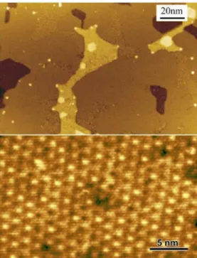
Fig. 3-8. Atomic force microscope image of atomic layer deposition on graphene. ... 50
Fig. 3-9. Cross-sectional high resolution transmission electron microscope image of the Al2O3 oxide grown on graphene film by using ALD... 50
Fig. 3-10. EDX analysis of Al2O3 grown by ALD (From the cross-section of blue line in Fig 3-9). ... 51
Fig. 3-11. IDS-VGS curve of sample 01 (Recipe I). ... 51
doi:10.6342/NTU201600721
XV
Fig. 3-12. IDS-VGS curve of sample 02 (Recipe II). ... 53
Fig. 3-13. IDS-VGS curve of sample 03 (Recipe III). ... 53
Fig. 3-14. IDS-VGS curve of sample 04 (Recipe IV). ... 54
Fig. 3-15. IDS-VGS curve of sample 05 (recipe V). ... 56
Fig. 3-16. IDS-VGS curve of sample 06 (recipe VI). ... 56
Fig. 3-17. The process flow chart graphene transfer process. ... 59
Fig. 3-18. Optical image of dual-gated graphene transistor. ... 62
Fig. 3-19. Device structure of dual-gated graphene transistor. ... 62
Fig. 3-20. IDS-VGS curve of sample 07 (bottom-gated transistor). ... 63
Fig. 3-21. IDS-VGS curve of sample 08 (ALD Al2O3 on bottom-gated transistor) ... 63
Fig. 3-22. IDS-VGS curve of sample 09 (bottom-gated transistor of dual-gated structure). ... 65
Fig. 4-1. Atomic force microscope image of sapphire (a) without annealing (b) annealed. ... 70
Fig. 4-2. The location of sample and sulfur powder. ... 70
Fig. 4-3. The growth mechanism of MoS2. ... 72
Fig. 4-4. The process flow chart of MoS2 top-gated transistor. ... 72
Fig. 4-5. Optical microscope image of MoS2 top-gated transistor. ... 73
Fig. 4-6. Device structure of MoS2 top-gated transistor. ... 73
doi:10.6342/NTU201600721
XVI
Fig. 4-7. IDS-VGS curve of sample 11. ... 74
Fig. 4-8. The process flow chart MoS2 transfer process. ... 78
Fig. 4-8. The process flow chart MoS2 transfer process. (Continued) ... 79
Fig. 4-9. Optical image of dual-gated MoS2 transistor. ... 79
Fig. 4-10. Device structure of dual-gated MoS2 transistor. ... 80
Fig. 4-11. IDS-VGS curve of sample 12 (bottom-gated transistor). ... 80
Fig. 4-12. IDS-VGS curve of sample 13 (ALD Al2O3 on bottom-gated transistor) ... 81
Fig. 4-13. IDS-VGS curve of sample 14 (bottom-gated transistor of dual-gated structure). ... 83
Fig. 4-14. IDS-VGS curve of sample 15 (top-gated transistor of dual-gated structure).... 83
doi:10.6342/NTU201600721
XVII
List of Tables
Table 1-1. Summary Table of ITRS Technology Trend Targets (Table taken from
International Technology Roadmap for Semiconductors [1]) ... 2
Table 1-2. Mobility and band gap comparison between Si and possible candidates. ... 4
Table 3-1. Experiment recipes for oxide optimization. ... 47
Table 3-2. Purpose of experiment between recipe 01 and recipe 02... 47
Table 3-3. Purpose of experiment between recipe 02 and recipe 03... 48
Table 3-4. Purpose of experiment between recipe 03 and recipe 04... 48
Table 3-5. Purposes and parameters of recipe 05 and recipe 06. ... 57
Table 3-6. Comparison and summary of top-gated graphene transistors. (Forward Swing). ... 57
Table 3-7. Device structure parameters of sequential dual-gated graphene transistor. .. 60
Table 3-8. Comparison and summary of graphene transistors. (Forward Swing). ... 66
Table 4-1. Device structure parameters of sequential dual-gated MoS2 transistor. ... 76
Table 4-2. Comparison and summary of MoS2 transistors. ... 84
doi:10.6342/NTU201600721
1
Chaper 1. Introduction
1.1. The Upcoming End of Scaling of Silicon MOSFETs
For decades, Moore’s law has driven the semiconductor industry, a reduction of the cost per transistor by 25 % every year. Successfully scaling of Silicon-based metal oxide field effect transistor (MOSFET) is the main driven force. For now, 16-nm gates Silicon-based MOSFET is in mass production. In the expectation of International Technology Roadmap for Semiconductors (ITRS), 7-nm MOSFET is needed in 2017 (Table 1-1) [1]. However, the scaling of Si MOSFET becomes more difficult while device performance needs to be satisfied at the same time. Issues such as short channel effects, parasitic capacitance and gate leakage current have arose to slow down Moore’s Law. To overcome these problems, new MOSFET structure has been developed such as tri-gate MOSFETs. While new structure of MOSFET has alleviated the problem of
facing the physical limitation in a short time, further scaling of MOSFET is still critical for extension of the lifetime of Moore’s law and the future of semiconductor electronics
industry. Therefore, chipmakers and researchers have dedicated to finding new materials for even smaller transistors.
doi:10.6342/NTU201600721
2
Table 1-1. Summary Table of ITRS Technology Trend Targets (Table taken from International Technology Roadmap for Semiconductors [1])
doi:10.6342/NTU201600721
3
1.2. Development and Rationale of Two-dimensional Materials
There are several candidates (Table 1-2) for the post-Si era of semiconductor industry such as Ge, III-V and two-dimensional materials including graphene and transition metal dichalcogenides (TMDs). Two-dimensional materials have drawn great attention for researchers and engineers in the last decade because of their amazing characteristics exhibited in several atomic layers. Two-dimensional materials emerge from the successful fabrication of monolayer graphene by mechanical exfoliation done by the research group of A. K. Geim and K. S. Novoselov from the University of Manchester (Fig. 1-1). Since then, not only graphene but also brand new two-dimensional materials such as MoS2 are explosively investigated.
Two-dimensional materials have layered structure. One single layer of two-dimensional material has the thickness below nanometer scale, for example, graphene is ~0.4 nm and MoS2 is ~0.7 nm per monolayer. Two-dimensional materials also have high thermal stability comparing with Si, providing a good compatibility for nowadays semiconductor fabrication process. Two-dimensional materials are also possible for the flexible device fabrication, where other competing materials such as Ge and III-V materials cannot, giving a very good characteristic for bendable applications.
doi:10.6342/NTU201600721
4
Fig. 1-1. The first successfully fabricated monolayer graphene and experimental devices.
(Fig. taken from K. S. Novoselev [2])
Material Si Ge GaAs Graphene MoS2
Electron
cm2/Vs 1600 3900 9200 15000 470
Hole
cm2/Vs 430 1900 400 15000 480
Band gap (eV)
1.12
(indirect) 0.66 1.42 0 1.9
(monolayer)
Table 1-2. Mobility and band gap comparison between Si and possible candidates.
doi:10.6342/NTU201600721
5
1.3. Fundamentals of Two-dimensional Materials
1.3.1. Basics of Graphene
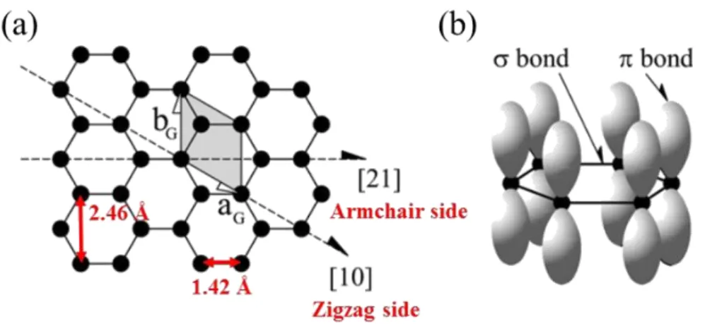
The graphene structure, single layer of carbon atoms arranged in a hexagonal 2-D lattice, is actually predicted as early as 1947 by Wallace at the time the word “graphene”
was not even existed. However, the existence is questioned by scientists because they believe that the atoms cannot form thermodynamically stable two-dimensional structure in ambient. At 2004, the group led by A. K. Geim and K. S. Novoselov has finally fabricate monolayer graphene using mechanical exfoliation method form highly oriented pyrolytic graphite (HOPG) [2], proving that monolayer graphene does exist in nature. The pioneering result has let Geim and Novoselov to win the Nobel Prize in
2010.
The word “graphene” is a combination of “graphite” and the suffix “–ene.”
Two-dimensional honeycomb crystal lattice in which one carbon atom forms each vertex composes graphene. In this hexagonal two-dimensional structure, each carbon
atom consists of three sp2 orbital hybridization. The carbon atom bonds with each other
-bond with the angle of 120o (Fig. 1-2) [3]. The lattice constant is 2.46 Å and the
carbon-carbon bond length is 1.42 Å .
Graphene has a unique band structure. As we can see in Fig. 1-2 (b) [3], 2s, 2px and
doi:10.6342/NTU201600721
6
Fig. 1-2. (a) Hexagonal structure of graphene. The unit cell is shaded with standard unit cell vectors aG and bG. (b) Carbon-carbon bonding in graphene with the in-plane σ
bonds and the π orbitals. (Fig. taken from J. Hass [3])
doi:10.6342/NTU201600721
7
2py constitutes sp2 orbital hybridization among four valence electrons of carbon (2s1p3)
forming a covalent bond (-bond) with an angle of 120oC while 2pz makes up the π-bond with adjacent carbon atom, enabling the electrons to hop and become
moving-free. The adjacent π-bonds hybridize together to form the π-band (valence band) and π∗-bands (conduction band) according to the calculation using tight bonding
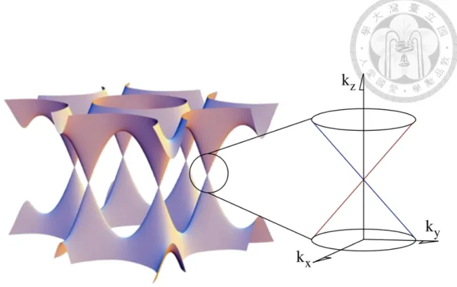
approximation model for monolayer graphene [4]. The conduction band and valence band meets at the edge of first Brillouin zone. At this point the density of state (DOS) is zero and is named charge neutrality point (CNP) or Dirac point (Fig. 1-3). Thus, graphene is a zero band gap semiconductor material in its nature.
There are several fabrication methods of graphene such as the mechanical exfoliation, epitaxial growth, the reduction from graphene oxides and the chemical vapor deposition (CVD). Mechanical exfoliation is the first approach to successfully fabricate monolayer graphene by A. K. Geim and K. S. Novoselov form The University of Manchester in 2004. Scotch tapes are used to peel off thin flake of graphite from HOPG. The thin flake is repeatedly peeled off further layers until there is only a few layer left. At last the thin layer of graphite is transferred to SiO2/Si substrate. The thickness can be determined using reflection and contrast spectroscopy as shown in Fig.
1-4 [5]. The graphene fabricated by mechanical exfoliation has high quality but with
poor film completeness and difficulties of precise control over the exact layer number.
doi:10.6342/NTU201600721
8
Fig. 1-3. The band structure of graphene shows six Dirac cones. (Fig. taken from J.
Hass [3])
Fig. 1-4. The optical microscope image of different layers of graphene on SiO2 (300nm).
(Fig. taken from Z. H. Ni [5])
doi:10.6342/NTU201600721
9
Mechanical exfoliation method is also disadvantageous for mass production. Therefore, the practical application of this approach is quite limited.
Graphene multi-layers can also be grown by epitaxial growth method on single crystal silicon carbide (SiC) by W. A. de Heer from Georgia Institute of Technology in 2007 [6]. The carbon-silicon covalent bond is broken by the energy provided when the substrate is heated up to 1600oC under ultra-high vacuum environment. Then, the dangling carbon atoms on the surface constitute carbon-carbon covalent bond and form graphene thin film, as shown in Fig. 1-5. The epitaxially grown graphene is of high quality and larger area compared with the mechanical exfoliation method. However, the uniformity and layer numbers are again difficult to control. The other issue is that SiC substrates are very expensive, which makes this method a rare chosen approach for graphene growth nowadays.
Reduction form graphene oxide is another way to fabricate graphene. Concentrated sulfuric acid is used as an oxidizing agent to oxidize HOPG bulk, forming abundant functional groups: phenyl, epoxy, carbonyl, etc. The HOPG bulk can be broken into graphene oxide flakes because the van der Waals force between layer and layer is reduced. Then strong reductant such as hydrazine and NaBH4 is used to remove functional groups and restore the structure or high temperature annealing is applied to obtain monolayer of multilayer graphene, as shown is Fig. 1-6 [7]. The graphene
doi:10.6342/NTU201600721
10
Fig. 1-5. The STM image of graphene grown by epitaxial growth method. (Fig. taken from W. A. de Heer [6])
Fig. 1-6. (a) Graphene fabricated by oxidizing bulk HOPG (b) Graphene fabricated by reduction using high temperature annealing. (Fig. taken from X. Li [7])
doi:10.6342/NTU201600721
11
fabricated by the reduction of graphene oxide has relatively lower quality because the lattice is damaged during oxidization and the incompleteness of reduction. Although this method is more suitable for mass production, the graphene film quality is not good enough for electronic and optoelectronic applications.
The last method to fabricate graphene is chemical vapor deposition (CVD). CVD is a common technique to fabricate high-purity and high-quality solid thin films. Injected gas undergoes chemical reaction or decomposition and then deposit on substrate.
Because of the low pressure environment, unnecessary reaction can be eliminated. Thus the film uniformity and quality can be greatly enhanced. The film can be grown in single crystalline, polycrystalline or amorphous form by the control of growth parameters. Graphene grown using CVD mainly uses carbon source (methane (CH4), acetylene (C2H2), etc.) and the source undergoes decomposition under high temperature with the help of metal catalyst. Eventually, the graphene can be deposited onto various substrates. Graphene can be grown on several different metals with high quality with precise thickness control. For example, Platinum (Pt) [8], Iridium (Ir) [9], Cobalt (Co) [10], Gallium (Ga) [11], Nickel (Ni) [12], and Copper (Cu) [13], [14]. Metalloid can be used to grow graphene, such as Germanium [15], [16]. Using metalloid as the substrate can avoid the transfer process needed when growing on metal substrate. Furthermore, the growth of graphene can be integrated into commercial semiconductor process.
doi:10.6342/NTU201600721
12
Nonmetal substrates can also be used to grow graphene. Our group has successfully fabricated graphene grown directly on sapphire substrate, as shown in Fig. 1-7 [17].
Also, our group can further grow other two-dimensional materials such as molybdenum disulfide (MoS2) on graphene/sapphire substrate, as shown in Fig. 1-8 [18].
1.3.2. Basics of MoS
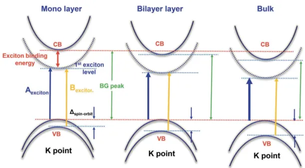
2In addition to graphene, TMDs are a best-known member in the family of two-dimensional materials. TMDs are with the common chemical formula MX2 where M stands for a transition metal (M = Mo, W, etc.) and X for group VI atoms (X = S, Se or Te). The lattice is formed as a sandwich structure that the transition metal atoms are surrounded beneath and on the group VI atoms. Hexagonal honeycomb structure constitutes the two-dimensional structure (Fig. 1-9) [19]. Unlike the zero-bandgap graphene, MoS2 has layer-dependent band gap values. Bulk MoS2 has the indirect band gap of 1.2 eV while monolayer MoS2 has the direct band gap of 1.8 eV. Not only the number of layer but also the applied stress and electric field will affect the band gap values (Fig. 1-10) [20].
Conventional methods of fabricating MoS2 are through mechanical exfoliation and CVD. The mechanical exfoliation method is the following work with what A. K. Geim and K. S. Novoselov have done on graphene. Again, Scotch tapes are used to peel off
doi:10.6342/NTU201600721
13
Fig. 1-7. Growth mechanism of graphene directly grown on sapphire. (Fig. taken from M. Y. Lin [17])
Fig. 1-8. MoS2 grown on graphene/sapphire substrate. (Fig. taken from M. Y. Lin [18])
doi:10.6342/NTU201600721
14
Fig. 1-9. Structure of TMDs. (a) Top view (b) Front view. (Fig. taken from H. Zeng [19])
Fig. 1-10. Band gap modulation of MoS2 under different thickness. (Fig. taken from K.
P. Dhakal [20])
doi:10.6342/NTU201600721
15
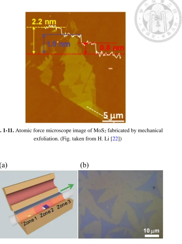
MoS2 flakes from bulk MoS2 repeatedly and, eventually, this makes MoS2 reach desired thickness. The MoS2 obtained by mechanical exfoliation has high quality and fine optoelectronics characteristic. The highest mobility can be as high as 200 cm2V-1s-1 [21].
However, problems such as incompleteness of thin film, uncontrollable thickness and difficulty for mass production still remained. An example of MoS2 fabricated by mechanical exfoliation transferred to SiO2 substrate is shown in Fig. 1-11 [22]. Lack of uniformity of thickness can be observed from the atomic force microscope image.
Another common way to fabricate MoS2 is through CVD. The CVD system is illustrated as Fig. 1-12 (a) [23]. Sulfur powder is placed at the entrance of the furnace while precursor, molybdenum oxide powder or MoCl5,and the substrate are placed in the middle of the furnace. The growth temperature is about 700 ~ 800 oC and with carrier gas like N2 or Ar to provide continuous gas flow. When the temperature is heated up to the growth temperature, the sulfur powder will evaporate and react with the precursor to form MoS2 on the substrate. High-quality MoS2 films can be grown by using CVD.
However, incomplete coverage and the non-uniform thickness are disadvantages of this approach (Fig. 1-12 (b)).
1.4. The Organization of the Thesis
This thesis focuses on the fabrication of top-gated transistors for both graphene and
doi:10.6342/NTU201600721
16
Fig. 1-11. Atomic force microscope image of MoS2 fabricated by mechanical exfoliation. (Fig. taken from H. Li [22])
Fig. 1-12. (a) Common chemical vapor deposition system for MoS2 growth (b) Single crystal MoS2 grown by chemical vapor deposition. (Fig. taken from B. Liu [23])
doi:10.6342/NTU201600721
17
MoS2. Top-gated transistors can avoid the transferring process, which leads to contamination and inconvenience for device fabrications. Also, the comparison of top-, bottom- and dual- gated transistor structure are also investigated in this thesis.
The organization of the thesis is briefed as follows. The introduction and motivation for this thesis is stated in the first chapter. In chapter two, the various equipment used in this thesis is introduced, including material growth systems, device process systems, material analysis systems and electrical characteristic measurement systems. In chapter 3, top-gated graphene transistor is first fabricated and investigated.
Atomic layer deposition technique is adopted for top dielectric layer growth. Then, the comparisons of top-, bottom- and dual-gated transistor structures are investigated. In chapter four, the developed top-gated transistor fabrication process is applied to MoS2. Then, the comparisons of top-, bottom- and dual-gated transistor structures are investigated.Finally, a conclusion and future work plan is given in chapter five.
doi:10.6342/NTU201600721
18
Chaper 2. Introduction of Experimental Instruments
2.1. Material Growth and Device Fabrication Instruments
2.1.1. Low Pressure Chemical Vapor Deposition System (LPCVD)
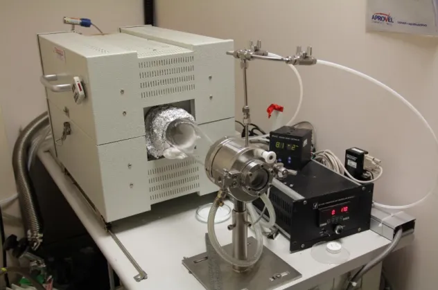
The LPCVD system provides a way to deposit high-purity and high-quality solid thin films. The injected gas undergoes chemical reaction or chemical decomposition on substrates and then deposit onto them in hot furnace under low pressure. With the control of parameters such as temperatures and the chamber pressure, single crystal, polycrystalline or amorphous solid films can be deposited. In this thesis, the LPCVD system is used to grow graphene films directly on sapphire substrates. The LPCVD
system in our laboratory is further introduced as follows (Fig. 2-1).
High temperature furnace
The high temperature furnace undergo a heating process from room temperature to 1100 oC in 2 h (heating rate: 9.17 oC/min) and then stay for 1 h annealing and graphene growth for 3 h. Then the heater is turned off and cool down to room temperature (Fig. 2-2).
A 2 inch quartz tube is chosen as the chamber for its thermal stability under 1100
doi:10.6342/NTU201600721
19
Fig. 2-1. LPCVD system for graphene growth.
Fig. 2-2. Temperature-Time curve of LPCVD graphene.
doi:10.6342/NTU201600721
20 oC. The sample holder is also made of quartz.
Mass flow controller (MFC)
The MFC controls the mass flow of gas precisely. The unit of mass flow is standard cubic meter per minute (sccm) which is defined as the number of moles of
gas passing through one mL under 1 atm at 273 K per minute.
LPCVD chamber
The LPCVD chamber is composed of a quartz tube, a mechanical pump, a capacitance manometer and gate valve. The mechanical pump can pump down the chamber to a pressure lower than 5 × 10⁻³ torr. The manometer can sense the pressure of the system from 10-3 ~ 760 torr.
The reaction equation of chemical vaper deposition is as follows.
CH4 → C + 2H2 (1100 oC) (2-1) The mechanism is illustrated in Fig 2-3 [24]. Methane is first decomposed at 1100
°C in the hot furnace. The decomposed carbon atoms are then colliding with each other and undergo homogeneous nucleation, forming graphene flakes in gaseous environment.
With continuous growth, the flakes are growing bigger and bigger before they finally fall down onto the substrate. In addition, the reason why graphene film is grown layer by layer is that the graphene/graphene adhesion is weaker than that between graphene and the substrate, so most of the graphene flakes are blown away by the carrier gas (Ar)
doi:10.6342/NTU201600721
21
Fig. 2-3. Growth mechanism of graphene. (Fig. taken from M. Y. Lin [24])
doi:10.6342/NTU201600721
22
before the substrate is fully covered by the first few layers of graphene.
2.1.2. Transition Metal Deposition System: Radio-frequency (RF) Sputtering Deposition System
The MoS2 film is synthesized by a two-step process. The transition metal, Molybdenum (Mo), is deposited by a radio-frequency sputtering deposition system first.
The sputtering system enables high energy particle to bombard the surface of target and force the particle to deposit onto the substrate. The system used for this thesis is introduced as follows (Fig. 2-4).
The sputtering system consists of three main parts: the vacuum chamber, rough pump and high vacuum pump. The sputtering deposition process needs to be done under high-vacuum condition. Therefore, a mechanical pump as a rough pump to pump down the chamber to 3 × 10⁻² torr. Then, a diffusion pump as a high vacuum pump continuously pump down the chamber to the working pressure ~ 3 × 10⁻⁶ torr.
The selection of manometer is important in the sputtering system. The pressure changes from atmosphere to high vacuum within the whole sputtering deposition process. Two stage manometers are chosen to fit different pressure ranges. When the chamber is undergoing rough pump down, Pirani Gauge is used to measure the pressure.
A Pirani Gauge can detect the pressure range from 760 torr to 10-3 torr. After the system
doi:10.6342/NTU201600721
23
Fig. 2-4. Radio-frequency (RF) Sputter Deposition System.
doi:10.6342/NTU201600721
24
is switched to high vacuum pump down process, a Hot Cathode Ionization Gauge is used to measure the pressure. A Hot Cathode Ionization Gauge has a measurement range from 10-3 torr to 10-10 torr.
The sputtering gun of the system provides a maximum output power up to 300 W.
When the pressure is pumped down to 3 × 10⁻⁶ torr, the sputtering process can start.
Argon (Ar) gas is injected to the chamber and the RF power is gradually increased. The Ar gas will be ionized and start bombarding the surface of the target. Once the power is large enough, the particle of the target can be ejected from the surface and deposit onto the substrate.
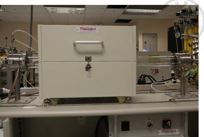
2.1.3. Transition Metal Sulfurization System:
After the Mo film is deposited by the sputtering system, sulfurization is needed to synthesize MoS2 films. The sulfurization system in our laboratory is shown in Fig. 2-5.
A 2-inch quartz tube is covered by a high temperature furnace with a door at the front side and connected with mechanical pump on the back side.
The chamber is pumped down by the mechanical pump first and then injected with Ar gas, creating a gas flow from front side toward back side. Then, the sample is placed at the location of 800 oC of the heater and the sulfur powder is placed at the location at the entrance of heater, where the temperature reading is 160 oC. The sulfur powder is
doi:10.6342/NTU201600721
25
Fig. 2-5. The transition metal sulfurization system
doi:10.6342/NTU201600721
26
vaporized after heating up and then carried by gas flow through the surface of the sample. Sulfur reacts with the pre-deposited the Mo metal and form MoS2 thin film. The mechanism of MoS2 growth is illustrated in Fig. 2-6.
The equation is shown as follows.
S2(s) → S2(g) (160oC)
Mo(s) + S2(g) → MoS2(s) (800oC) (2-2)
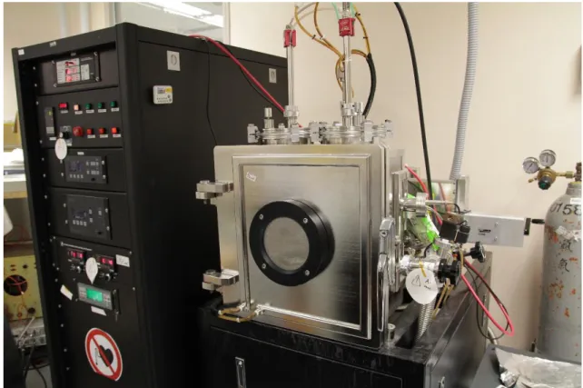
2.1.4. Electron beam Evaporation Physical Vapor Deposition System (EBPVD)
The metal contacts of all the devices in this thesis are deposited by an EBPVD system. The target metal placed at anode in a crucible in an EBPVD system is bombarded by an electron beam forming by a charged tungsten filament under high vacuum. The EBPVD system is a semi-automatic system (Fig.2-7). The system will automatically pump down after the sample and target are loaded. The system is equipped with a mechanical pump for rough pump and a cryopump for high vacuum pump with a automatic switch system. After the pressure reaches 3 × 10⁻⁶ torr, the filament is applied with increasing voltage until the target metal is transformed into gaseous phase and deposited onto the substrate.
doi:10.6342/NTU201600721
27
Fig. 2-6. The process flow of MoS2 growth: (a) Mo deposited on sapphire by the RF sputtering system, (b) Mo/sapphire undergoes sulfurization and (c) MoS2 is grown on
sapphire substrates.
Fig. 2-7. The EBPVD system.
doi:10.6342/NTU201600721
28
2.1.5. Reactive-Ion Etching (RIE) System
RIE is a common dry etching technique used in microfabrication. The material on surface is reacted and etched away by high-energy ions from plasma which is generated by electromagnetic field under vacuum. Specific gas is chosen for etching of specific material. The etching rate can be controlled by parameters such as the gas flow, the working pressure and the output power.
The system used in this thesis is a semi-automatic system (Fig. 2-8). It is equipped with a mechanical pump for rough pump and a turbo molecular pump for high vacuum pump. After the chamber is pumped down to 4.5 × 10⁻⁵ torr, the reacting gas will then injected to the chamber and controlled at a set working pressure. Gas flow being stable, the set power output will generate electromagnetic field and forming plasma. A cleaning recipe is done first to make sure the chamber is cleaned.
2.1.6. Atomic Layer Deposition (ALD) System
ALD has emerged as a promising technique for high quality thin film deposition.
ALD can provide ultrathin film growth with high quality, precise thickness control in the monolayer level and good uniformity over large area. ALD reaction needs two precursor reacting with each other to form the desired film but only one precursor is exposed to the surface. The reaction takes places on the surface sequentially and in a
doi:10.6342/NTU201600721
29
Fig. 2-8. The RIE system.
doi:10.6342/NTU201600721
30
self-limiting manner. Trimethylaluminum (TMA) and H2O are chosen as the precursor for Al2O3 growth by using ALD. The basic mechanism of ALD follows the four sequential steps to form an ALD cycle. (1) Precursor A (TMA) is injected into the chamber and coating to the surface of the substrate. (2) After the adsorption of precursor on the surface, excess precursor is removed by purging the chamber. (3) Precursor B (H2O) is injected into the chamber and reacts with precursor A to form the desired layer (Al2O3). (4) Excess precursor B is cleaned by purging the chamber. After the above 4-step cycle is done, a new cycle begins until the desired thickness is reached (Fig. 2-9) [25]. The overall reaction equation is as follows.
2Al(CH3)3 + 3H2O → Al2O3 + 3CH4 (2-3) The ALD system used in this thesis is a customized thermal ALD system manufactured by SYSKEY technology (Fig. 2-10). The system is composed of a chamber, vacuum pump system and a precursor module. The chamber substrate is a heater that can heat up to 300 oC. A mechanical pump pumps down the chamber to 5 × 10⁻³ torr. The precursor module consists of two precursor tanks and two high-speed pulse valves controlling the injection of precursors. The temperature of the precursor tank for TMA is controlled by a circulation refrigerator system. N2 is the carrier gas used during the ALD process.
doi:10.6342/NTU201600721
31
Fig. 2-9. The illustration of ALD process (Fig. taken from H. K. [25])
Fig. 2-10. The ALD system.
doi:10.6342/NTU201600721
32
2.2. Characterization Instruments
2.2.1. High Resolution Confocal Raman Spectroscopy
The Raman spectroscopy is a technique to investigate vibrational and rotational modes of lattice and molecules. Raman scattering is usually triggered by laser ranging from near infrared to near ultraviolet. This Raman spectroscopy is commonly used in chemistry now to identify chemical bonds, symmetry of molecules and quality of the sample in an efficient and non-destructive manner. The sample needs no special preparation and can be either in solid phase, liquid phase or gaseous phase.
The Raman effect which is the wavelength between incident and reflected light has slightly different when light passes through a transparent material is observed by Indian scientist Sir C. V. Raman in 1928. The observed different wavelengths are the Raman Shift.
The system used in this thesis is the HORIBA JobinYvon HR800UV, as shown in Fig. 2-11, in Nano Facility Center, National Chiao Tung University. Three different
wavelengths of triggering lasers, 488 nm, 532 nm and 632.8 nm, are equipped in this system. The 488 nm laser is used as the incident laser. The focused laser spot is about 6~7 m. So very fine information of material can be observed.
doi:10.6342/NTU201600721
33
Fig. 2-11. The high Resolution Confocal Raman Spectroscopy (HORIBA JobinYvon HR800UV).
doi:10.6342/NTU201600721
34
2.2.2. Transmission Electron Microscope (TEM)
Transmission Electron Microscope (TEM) is a technique that uses a beam of electron to transmit through an ultra-thin specimen and interact with the specimen when passing through. The transmitted electron is collected and magnified to form an image.
The specimen must be thinner than 2 Å to allow the electrons to transmit. Both elastic scattered electrons and inelastic scattered electrons can be collected. The former are electrons without energy lost so the information of internal structure can be obtained while the latter are the electrons with energy lost which corresponds to different lattice constant and can be further used for elemental analysis and lattice structure. Also, the electron diffraction pattern can be obtained by Fourier transform to analyze the lattice structure of the sample. With the help of energy dispersive spectrometer (EDS), the elemental analysis or chemical characterization of a specimen can be analyzed.
The cross-sectional high-resolution TEM with specimen preparation and
measurements are done by Material Analysis Technology, Inc. The photo of FEI Tecnai™ G2 F-20 is shown in Fig. 2-12.
2.2.3. Atomic Force Microscope (AFM)
Atomic Force Microscope (AFM) is a powerful and useful tool to examine the surface and roughness of the specimen. Unlike optical microscope or SEM, AFM
doi:10.6342/NTU201600721
35
Fig. 2-12. The FEI Tecnai™ G2 F-20 system (Fig. taken from MA-tek).
doi:10.6342/NTU201600721
36
gathers information by “touching” the sample through a probe. The accurate
piezoelectric element will detect the displacement and movement and form an image of the topography of the specimen surface at a high resolution. To investigate the surface of our sample, “tapping mode” is used in this thesis. The resonant frequency of the probe is set first. When the probe is move close to our surface of the sample, the probe will be affected by different Van der Waals force because of the topology of the surface.
Then the laser beam will detect the movement of the probe and provide the information of the surface. The surface roughness can also be obtained by AFM software. The AFM used in the thesis is BRUKER Dimension ICON (Fig. 2-13).
doi:10.6342/NTU201600721
37
Fig. 2-13. The AFM system (BRUKER Dimension ICON).
doi:10.6342/NTU201600721
38
Chaper 3. Top-gated Graphene Transistors Fabricated on Graphene Grown Directly on
Sapphire Substrates
Top-gated transistor structure can avoid the common film transferring procedure usually required for two-dimensional material device fabrication process. So film damages and contamination can be greatly reduced. Top-gated structure also provide a possibility of CMOS-compatible fabrication process which is very important for massive production. Graphene film is first grown directly on sapphire substrates and then fabricated into transistors. After fabrication, the devices performance is investigated in detail. Oxide deposition is especially a critical step in top-gated transistor. Therefore, growth optimization for the oxide layer is investigated. Also, the comparison between top- and bottom-gated transistors is investigated in this chapter.
3.1. The Fabrication Procedure of Top-gated Graphene Transistors
The fabrication procedure of top-gated graphene transistors can be divided into two parts: the growth of the graphene film and the device fabrication procedure. These two steps are further described in the following sub-sections.
doi:10.6342/NTU201600721
39
3.1.1. The Growth of Graphene Films Directly on Sapphire Substrates
The substrate chosen for graphene growth is (001) single crystal sapphire substrate, which has a melting point of 2072 oC under ambient environment. The graphene film directly grown on sapphire substrates is prepared by low pressure chemical vapor deposition system by the following steps. First, the sapphire substrates are cleaned by acetone and isopropanol using ultrasonic cleaning system. Then the sapphire substrates are loaded into a quartz tube of a low pressure chemical vapor deposition system and then pump down to 5 × 10⁻³ torr. After the pressure is reached, 500 sccm Ar gas is injected into the tube and is heated to 1100 oC. After the temperature is reached, the sample is stayed and undergo annealing for 1 h. The LPCVD system was then applied to grow graphene directly on the substrate for 3h Ar, H2 and CH4 mixture gas and the flow are 175, 225, and 30 sccm at the chamber pressure 2.9 torr. The graphene film grown directly on sapphire is shown in Fig. 3-1, the left sample is before graphene growth; the right sample is after graphene grown on the sapphire substrate. The Raman spectrum of the graphene film is shown in Fig. 3-2. Although exact layer number cannot be verified through the Raman spectrum, the more intense 2D peak intensity compared with G peak suggests that the film is of few-layer graphene. On the other hand, the weak D peak in the Raman spectrum suggests that a graphene film with high quality is obtained by using this growth technique [26][27][28]. To further investigate the layer number of the sample, the
doi:10.6342/NTU201600721
40
Fig. 3-1. The graphene film directly grown on sapphire.
(Left: sapphire before graphene growth; Right: graphene grown on sapphire).
Fig. 3-2. The Raman spectrum of graphene film directly grown on sapphire.
doi:10.6342/NTU201600721
41
cross-sectional HRTEM image of the sample is shown in Fig. 3-3. As shown in the figure, bi-layer graphene film is obtained for the sample.
3.1.2. The Device Fabrication Procedure of the Graphene Transistors
The source and drain pattern is defined by photolithography. Ti 5 nm and Au 50 nm are deposited sequentially as the source and drain contacts by the E-beam evaporator
system. The size of source and drain metal pad is 80 × 80 m2. The channel (width: 40
m; length: 50 m) is then defined by photolithography and etched away by reactive ion
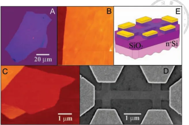
etching system. (Oxygen: 30 sccm; power: 50 W; time: 30 s; pressure: 1 × 10⁻² torr) The desired thickness of gate dielectric oxide (Al2O3, 30 nm) is deposited by the atomic layer deposition system. Finally, 5 nm Ti and 50 nm Au are deposited as the gate metal (length:
30 m) by the E-beam evaporation. The process flow chart, optical microscope image and the structure of the fabricated device is shown in Fig. 3-4, Fig. 3-5 and Fig. 3-6, respectively.
3.2. Growth Optimization of Al
2O
3Dielectric Layers on Graphene and Device Performances of Top-gated Graphene Transistors
There are several ways of oxide deposition nowadays, such as chemical vapor
doi:10.6342/NTU201600721
42
Fig. 3-3. The high-resolution transition electron microscope image of graphene film directly grown on sapphire.
Fig. 3-4. The process flow chart of graphene top-gated transistor.
(a) S/D metal deposition (b) channel definition (c) Oxide deposition (d) Gate metal deposition.
1000 1500 2000 2500 3000
Raman shift (cm
-1)
Intensity (a .u.)
D
G
2D
2 nm
Glue
Sapphire
0.3 nm 0.3 nm
(b)
(a)
doi:10.6342/NTU201600721
43
Fig. 3-5. Optical microscope image of graphene top-gated transistor.
(Top view. LG = 30 m; W= 10 m)
Fig. 3-6. Device structure of graphene top-gated transistor.
10 m
30 m
doi:10.6342/NTU201600721
44
deposition (CVD), plasma-enhanced chemical vapor deposition (PECVD), E-beam evaporation, sputtering deposition and atomic layer deposition (ALD). Among them, ALD is the state-of-art technique which can grow thin and high-quality oxide without introducing damages to substrates with its low growth temperature. Additionally, ALD can provide a precise control of oxide thickness to the atomic layer scale.
To grow a desired oxide as a gate dielectric layer of transistors, the oxide layer needs to be thin, providing good electrical field control and strong barrier of gate leakage currents. The material chosen in this thesis is Al2O3, grown by using the ALD technique
using Trimethylaluminum (TMA) as precursor and H2O as reactant.
Growth recipe optimization
Atomic layer deposited Al2O3 is a well-developed process for substrates like Si.
However, atomic layer deposited Al2O3 on two-dimensional material such as graphene is still under development. We have designed a series of experiments to optimize the oxide growth conditions on graphene.
The precursor tank and substrate heater is set to the desired temperature and wait until stable. Afterward the sample is loaded, then the chamber is first pump down to 5 × 10⁻³ and stay for 5 min before growth. When the countdown is over, cycles of Al2O3
growth started. One cycle consists of the following four steps: (1) precusrsor TMA is first pulsed into the chamber for the duration we set, (2) the chamber undergoes a purge
doi:10.6342/NTU201600721
45
process of N2 for 10 s, (3) reactant H2O is pulsed into the chamber for the duration we set and (4) the chamber undergoes the other purge process of N2 for 10 s (Fig. 3-7).
The recipes are listed in Table 3-1. All four recipes are designed at a growth temperature of 180 oC. Precursor temperature is set at 10 oC with 20 ms TMA + 20 ms H2O per cycle and a 250 sccm carrier gas (N2) flow in recipe I. Precursor temperature is set at 20 oC with 20 ms TMA + 20 ms H2O per cycle and a 250 sccm carrier gas (N2) flow in recipe II. Precursor temperature is set at 20 oC with 60 ms TMA + 60 ms H2O per cycle and a 250 sccm carrier gas (N2) flow in recipe III. Precursor temperature is set at 20 oC with 60 ms TMA + 60 ms H2O per cycle and a 20 sccm carrier gas (N2) flow in recipe IV. Comparison between recipe I and II is designed for different precursor temperature (Table 3-2). The precursor temperature will affect the vapor pressure of the TMA precursor, affecting the amount of precursor entering the chamber in the same pulse duration. Sufficient amount of precursor is required to cover the whole surface of the substrate at the TMA exposure step. Comparison between recipe II and III is designed to investigate whether the dosage is sufficient in different pulse duration (Table 3-3). Insufficient precursor will leads to poor coverage. Comparison between recipe III and IV is designed to investigate the influence of carrier gas flow (Table 3-4).
If the gas flow is not sufficient, precursor and reactant is not evacuated completely, thus, affecting the quality of grown oxide.
doi:10.6342/NTU201600721
46
Fig. 3-7. Process illustration of atomic layer deposition.
doi:10.6342/NTU201600721
47
Sample No.
Recipe No.
Substrate Temperature
(oC)
Precursor (TMA) Temperature
(oC)
Precursor Recipe
N2 Carrier Gas Flow (sccm)
01 I 180 10
20 ms TMA + 20 ms H2O
250
02 II 180 20
20 ms TMA + 20 ms H2O
250
03 III 180 20
60 ms TMA + 60 ms H2O
250
04 IV 180 20
60 ms TMA + 60 ms H2O
20
Table 3-1. Experiment recipes for oxide optimization.
Sample No.
Recipe No.
Substrate Temperature
(oC)
Precursor (TMA) Temperature
(oC)
Precursor Recipe
N2 Carrier Gas Flow (sccm)
01 I 180 10
20 ms TMA + 20 ms H2O
250
02 II 180 20
20 ms TMA + 20 ms H2O
250 Purpose: Investigate the vapor pressure of the TMA precursor, which affects the amount of
precursor entering the chamber in the same pulse duration.
Table 3-2. Purpose of experiment between recipe 01 and recipe 02.
doi:10.6342/NTU201600721
48
Sample No.
Recipe No.
Substrate Temperature
(oC)
Precursor (TMA) Temperature
(oC)
Precursor Recipe
N2 Carrier Gas Flow (sccm)
02 II 180 20
20 ms TMA + 20 ms H2O
250
03 III 180 20
60 ms TMA + 60 ms H2O
250 Purpose: Investigate whether the dosage is sufficient in different pulse duration.
Table 3-3. Purpose of experiment between recipe 02 and recipe 03.
Sample No.
Recipe No.
Substrate Temperature
(oC)
Precursor (TMA) Temperature
(oC)
Precursor Recipe
N2 Carrier Gas Flow (sccm)
03 III 180 20
60 ms TMA + 60 ms H2O
250
04 IV 180 20
60 ms TMA + 60 ms H2O
20
Purpose: Investigate the influence of carrier gas flow.
Table 3-4. Purpose of experiment between recipe 03 and recipe 04.
![Fig. 1-8. MoS 2 grown on graphene/sapphire substrate. (Fig. taken from M. Y. Lin [18])](https://thumb-ap.123doks.com/thumbv2/9libinfo/9605455.631516/31.892.138.760.392.908/fig-mos-grown-graphene-sapphire-substrate-fig-taken.webp)