1
vc vc3 vc5
2
vc vc4 vc6
D1 D2 D3 D4 D5 D6
vs
RL vo
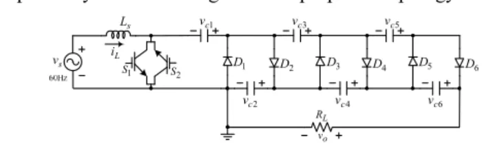
Fig. 1: The traditional three-stage Cockcroft-Walton rectifier
1
vc
2
vc 3
vc
4
vc 5
vc
6
vc
D1 D2 D3 D4 D5 D6
S2
Ls
iL
vs
S1
RL vo
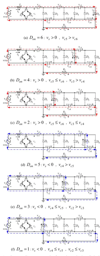
Fig. 2: The proposed converter with three-stage Cockcroft-Walton rectifier
A novel single-phase ac to high voltage dc converter bas ed on Cockcroft-Walton cascade rectifier
Chung-ming Young and Ming-hui Chen
Department of Electrical EngineeringNational Taiwan University of Science and Technology Taipei, Taiwan, R. O. C. 106
Email: [email protected]
Abstract—This paper proposes a novel single-phase ac to high voltage dc converter based on Cockcroft-Walton cascade rectifier with only adding one bi-directional switch and one boost inductor.
This paper also derives a new method of circuit representation for Cockcroft-Walton cascade rectifier, which simplifies the equivalent circuit and is convenient for simulation. Compared with conventional Cockcroft-Walton rectifier, the proposed converter provides half- wave symmetric and low-distorted line current, adjustable power factor at the ac source, and regulated dc output voltage. Unit power factor is achieved by the average-current method and the dc output voltage is regulated by a PI compensator. Moreover, this paper employs a digital signal processor to implement a digital controller for operating the proposed converter and a prototype with 500w rating is implemented for test. Both simulation and experimental results demonstrate the validity of the proposed converter.
Keywords-Cockcroft-Walton rectifier; high voltage dc converter;
bi-directional switch; power factor correction
I. INTRODUCTION
High voltage dc power supplies have widely applied in industries, science, medicine, military, and especially in test equipments, such as X-ray systems, dust-filtering, insulating test, and electrostatic coating [1]. Providing the advantages of compactness and cost efficiency, Cockcroft-Walton rectifier, which is constructed by a cascade of capacitors and diodes, is very popular among high voltage dc applications [2]. However, traditional Cockcroft-Walton rectifier has some shortcomings, such as high-distorted and half-wave-asymmetric line current, unregulated output voltage, and a large amount of ripples [3].
Recently, a number of high-frequency switching techniques for the Cockcroft-Walton rectifier have been introduced to reduce the amount of ripples of output voltage for single-phase system, but still have not improved the line current distortion problems [4]. Some power factor correction techniques for Cockcroft-Walton rectifier are developed by the two-stage circuit to improve the line current distortion problems.
Nevertheless, two-stage topologies incur higher cost and loss [5].
A three-stage conventional Cockcroft-Walton rectifier and the proposed converter are shown in Fig.1 and Fig.2,
respectively. The advantages of the proposed topology are as
follows:
1) The line current waveform has half-wave symmetry and low distortion which conventional Cockcroft-Walton rectifier can’t achieve.
2) At any given instant, there is only one conducting semiconductor device in the power flow paths.
3) Providing high step up rate without using a boost transformer.
4) The control method of conventional boost converter can be adapted for use by the proposed converter easily [6].
This paper also derives a new method of circuit representation, which will be detailed in section II, for Cockcroft-Walton cascade rectifier. This new circuit representation simplifies the equivalent circuit and is convenient for digital simulation. The control of power factor correction and dc output voltage regulation are presented in section III. For verification, this paper employs a digital signal processor (TMS320LF2407) to implement a digital controller for the proposed converter and a prototype with 500w rating is implemented as well. Both simulation and experimental results
2 vc
3 vc 4
vc 5 vc 6 vc 1 vc
2
iD 4
iD 6
iD
(a)
2 vc 3 vc
4 vc 5 vc
6 vc 1 vc
5
iD iD3 iD1
1
vc
2
vc 3
vc
4
vc 5
vc
6
vc
D1 D2 D3 D4 D5 D6
S2
Ls
iL
vs
S1
RL vo vd
D6 i
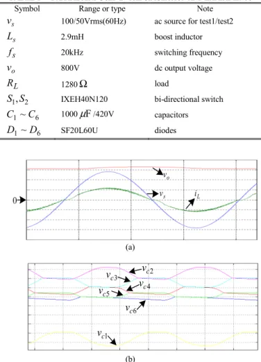
(a) Don=6: vs>0,vc5>vc6
1
vc
2
vc 3
vc
4
vc 5
vc
6
vc
D1 D2 D3 D4 D5 D6
S2
Ls
iL
vs
S1
RL vo vd
D4
i
(b) Don =4: vs>0,vc5≤vc6,vc3>vc4
1
vc
2
vc 3
vc
4
vc 5
vc
6
vc
D1 D2 D3 D4 D5 D6
S2
Ls
iL
vs
S1
RL vo vd
D2
i
(c) Don =2: vs>0,vc5≤vc6,vc3≤vc4
vd
D5
i 1
vc
2
vc 3
vc
4
vc 5
vc
6
vc
D1 D2 D3 D4 D5 D6
S2
Ls
iL
vs
S1
RL vo
(d) Don =5:vs<0,vc4>vc5
vd
D3
i 1
vc
2
vc 3
vc
4
vc 5
vc
6
vc
D1 D2 D3 D4 D5 D6
S2
Ls
iL
vs
S1
RL vo
(e) Don =3:vs<0,vc4≤vc5,vc2>vc3
1
vc
2
vc 3
vc
4
vc 5
vc
6
vc
D1 D2 D3 D4 D5 D6
S2
Ls
iL
vs
S1
RL vo vd
D1
i
(f) Don =1:vs<0,vc4≤vc5,vc2≤vc3
Fig. 4: Corresponding current paths for each conducting diode in sequence. (a) Current path ofiD6. (b) Current path ofiD4. (c) Current path ofiD2. (d) Current path ofiD5. (e) Current path ofiD3. (f) Current path ofiD1.
are shown In section IV. Finally, in section V conclusion is presented.
II. ANALYSIS OF OPERATION
Fig.2 shows the proposed converter, which is supplied by a utility ac source. The proposed converter consists of a boost inductorL , a bi-directional switch(s S ,1 S ) with 2 S operating 1 in positive-half cycle of the source and S operating in the 2 negative-half cycle of the source, and a three-stage Cockcroft- Walton rectifier in this case. The well-known rectifier is constructed by a cascade of stages with each stage containing two capacitors and two diodes. For an N/2-stage (N is an even number) Cockcroft-Walton rectifier, there are N capacitors and N diodes. For convenience, both capacitors and diodes are divided into odd group and even group, as denoted in Fig. 2.
In order to study the steady-state behavior for the proposed converter, the diode conducting condition of the traditional Cockcroft-Walton rectifier is described first. Through simulation, the capacitor voltages and diode currents are shown in Fig. 3(a) for positive-half cycle and Fig. 3(b) for negative- half cycle respectively. It can be seen that even capacitors are charged and odd capacitors are discharged through even diodes in sequence during the positive-half cycle, and vice versa during the negative-half cycle. The conducting sequences are
D ,6 D and4 D in the positive-half cycle and 2 D ,5 D and3 D 1 in the negative-half cycle respectively. Fig. 4 shows the corresponding current paths for each conducting diode with Fig.
4(a)-(c) for positive-half cycle and Fig. 4(d)-(f) for negative- half cycle. Two diode conducting phenomena are found: 1) there is at most one conducting at any instant, 2) the sequence of conducting diode is from right side to left side with even diodes conducting in positive-half cycle and odd diodes conducting in negative-half cycle.
According to above description, this paper derives a new mathematic method to analyze the operating of Cockcroft- Walton rectifier more generally and systematically. First, we introduce the diode-conducting indexDon to determine which diode is conducting and which current path should be taken.
Donis given by
vcel
RL
vo
Ls
iL
vs
d 1 0
0 1(1−d) vd
vcer
vcol vcor
Fig. 5: The general equivalent circuit of the proposed converter
{ }
⎩⎨⎧−
=
=
<
= >
1 , , ...
...
, , 3 4 , , 1 2 , , 0 for 0
max N
N k
k v x v D
s s k
on (1)
where
{ }
xk is a set of possible conducting indexes and it elements are given by) ( ) 1 (
) ( ) 1 (
, 2
, 2
2
for for for
, 0
, ,
k c k c
k c k c k
v v
v v
k k k k k x
≤
>
>
>
≤
⎪⎩
⎪⎨
⎧
=
−
− (2)
where vc(k) is the voltage of the k-th capacitor and will be given later.
Although there are discontinuous-conduction and continuous-conduction modes that can be operated in this converter, only the latter is conducted in this paper. Let d be the conducting state of the bi-directional switch and is given by
( o and 0)
) 0 and on ( or or ) 0 and o (
) 0 and on ( , , 0 1
2 2 1
1
<
=
<
=
>
=
>
=
⎩⎨
=⎧
s s s
s
v ff S
v S
v ff S
v d S
(3) Consequently, Fig. 5 sketches the general equivalent circuit of the proposed converter and the differential equation of line current is given by
[
(1 )( )]
1
col cel s
s
L v d v v
L dt
di = − − − (4)
where
i
Lis the line current and vcel(vcol) represents the series voltage of even(odd) capacitors that are on the left side of the conducting diode. Both vcel andvcol are dependent on Don and are given by (5) and (6) respectively, where⎣ ⎦
y (⎡ ⎤
y ) is the largest (smallest) integer not larger (less) than y.⎣ ⎦
⎪⎩
⎪⎨
⎧
=
≠
= ∑=
1 for 0
1 for
2 / 1 (2)
on on D
i c i
cel
D D v v
on
(5)
⎡ ⎤
= ∑
= −
2 / 1 (2 1) Don
i c i
col v
v (6)
Moreover,
v
ce2andv
co2 represent the series voltages of even and odd capacitors respectively, that are on the right side of the conducting diode, and are given by (7) and (8).⎣ ⎦
⎣ ⎦
⎪⎩
⎪⎨
⎧
=
≠
= = ∑ +
N D
N D v v
on on N
D
i c i
cer on
for 0
for
2
/ 1 2
/ (2) (7)
⎡ ⎤
⎡ ⎤
⎡ ⎤ ⎡ ⎤
⎡ ⎤ ⎡ ⎤
⎪⎩
⎪⎨
⎧
=
≠
= = ∑ + −
2 / 2 / for 0
2 / 2 / for
2
/ 1 2
/ (2 1)
N D
N D
v v
on on N
D
i c i
cor on (8)
Summing (5) and (7), we can obtain the output voltagev , o the total voltages of all even capacitors,
cer cel
o v v
v = + (9) The current equations of each even and each odd capacitors are given by (10) and (11)
⎥⎦
⎢ ⎤
⎣
⎡ − ⋅ ⋅ −
=
L L o i i
ci
R i v d C d
dt
dv 1 (1 ) (10)
[
j L]
j
cj d d i
C dt
dv = −1(1− )⋅ ⋅ (11)
where Ci is the capacitance of the i-th even capacitor and C is the capacitance of the j-th odd capacitors, and j
d andi d are given by (12) and (13) j
i D
i d D
on on
i ≥
<
⎩⎨
=⎧ , , 1
0 for i=2,4,...,N (12)
j D
j d D
on on
j ≥
<
⎩⎨
=⎧ , , 1
0 for j=1,3,...,N−1 (13)
Whendi=0, C is on the right side of the conducting i diode and is discharging through the load. When di=1, C is i on the left side of the conducting diode and is discharging for
0 ) 1
( −d ⋅iL< or is charging for (1−d)⋅iL>0. Whendj=0, C is on the right side of the conducting diode and is floating. j
Whendj=1, C is on the left side of the conducting diode j and is charging for (1−d)⋅iL<0 or is discharging for(1−d)⋅iL>0.
From above derivation of the operation of the proposed converter, there are four operation modes of the proposed converter despite the number of the stages of the Cockcroft- Walton rectifier. Fig. 6 shows the equivalent circuits of the four operation modes with Fig. 6(a) and (b) corresponding to positive-half cycle and Fig. 6(c) and (d) corresponding to negative-half cycle. For Fig. 6(a) and (c), which are mode 1 and mode 3 withd=1, the boost inductor is charged by the ac source and the even-group capacitors supply the load. For Fig.
6(b), which is mode 2 withd =0, the boost inductor and the ac source transfer energy to the rectifier, and part of odd- capacitors are discharged while part of even-capacitors are charged. The charged and discharged capacitors are determined by Don. With the same energy transferring, the charging and discharging conditions of mode 4 are opposite to
vref
vo
us iL L*
* i iavg
vtri verr
vo
vs Ks
iL
2 1, S S
Fig. 7: The control scheme of the proposed converter with DPS-based digital controller.
vcel
RL
Ls
iL
vs
d 1 0
0 1(1−d) vd
vcer
vcol vcor
(a)
vcel
RL
Ls
iL
vs
d 1 0
0 1(1−d) vd
vcer
vcol vcor
(b)
vcel
RL
Ls
iL
vs
d 1 0
0 1(1−d) vd
vcer
vcol vcor
(c)
vcel
RL
vo
Ls
iL
vs
d 1 0
0 1(1−d) vd
vcer
vcol vcor
(d)
Fig. 6: Four operation modes of the proposed converter
vs iL vo
(a)
2
vc 3
vc
4
vc 5
vc 6
vc 1
vc
(b)
Fig. 8: Simulation results of the proposed system. (a) vs(25V/div), iL(12.5A/div), and vo(250V/div) waveforms. (b) voltage waveforms of each capacitor.
mode 2. It has to note that S is turned on in mode 1 and 1 S is 2
turned on in mode 3. Some switching strategies can be taken for improving line current condition and regulating the dc output voltage.
III. DIGITAL CONTROL STRATEGY
The control scheme of the proposed converter with digital controller is shown in Fig. 7, and there are two control loops, the voltage loop and current loop. The feedback signal of the output DC voltage, filtered through a low-pass filter for eliminating the line frequency ripple, is compared with set reference
v
ref . Then,v
err is fed to a proportional-integral controller to regulate the required reference currenti
avg*. Theunit line voltage signal
u
s is multiplied byi
avg* to obtain the reference signali
L* for the current loop. The output of currentTABLE1 PARAMETERS USED IN THE SIMULATION AND EXPERIMENTS
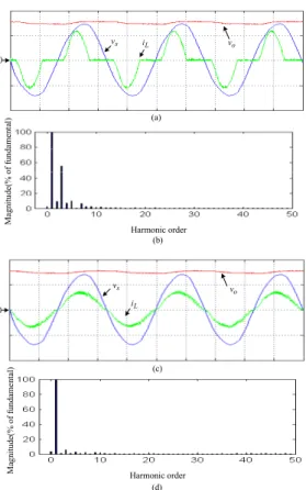
Symbol Range or type Note
vs 100/50Vrms(60Hz) ac source for test1/test2
Ls 2.9mH boost inductor
fs 20kHz switching frequency
vo 800V dc output voltage
RL 1280Ω load
2 1,S
S IXEH40N120 bi-directional switch
6 1~ C
C 1000μF/420V capacitors
6 1~ D
D SF20L60U diodes
compensator modulates with the triangular wave to generate PWM signals for the bi-directional switch. High-power-factor and low-distorted line current, and regulated dc voltage can be achieved consequently.
(a) 0
iL
vs vo
Harmonic order (b)
Magnitude(% of fundamental)
Harmonic order (d) vs
iL
vo
(c)
Magnitude(% of fundamental)
0
Fig. 9: Experimental results. (a) vs(100V/div), iL(10A/div), and vo(500V/div) waveforms for test1 andt: 5ms/div. (b) Spectrum of iL for test1. (c) vs(50V/div), iL(25A/div), and vo(500V/div) waveforms for test2. (d) Spectrum of iL for test2.
IV. Simulation and Experimental Results
Based on the mathematical model and control strategy described in section II and III respectively, a simulation program is conducted with the parameters shown in Table 1.
Fig. 8(a) shows the simulation results of v , s i , and L v , and o
Fig. 8(b) shows the voltages of each capacitor. The simulation results prove that the mathematical model can represent the proposed converter including the famous Cockcroft-Walton rectifier correctly. A 500w prototype is also built to verify the validity of the proposed converter. The system parameters used in the experiment are summarized in Table 1. For comparison, two tests with same output dc voltage and power are conducted. Test 1 is for the operation of conventional Cockcroft-Walton rectifier with 100Vrms/60Hz line voltage while test2 is for the operation of the proposed converter with 50Vrms/60Hz line voltage. Fig. 9(a) and (c) show the experimental results of v , s i , and L vo for test1 and test2 respectively, and the spectrums of i are shown in the Fig.9(b) L and (d) as well. From Fig. 9(b), it can be seen that the line current of conventional Cockcroft-Walton rectifier contains not only 58% 3rd harmonic but also about 10% and 7% of 2nd and 4th harmonic components, therefore the line current is
highly distorted and is not half-wave symmetric. The latter phenomenon, which rarely occurs in traditional diode-bridge rectifiers, is mainly caused by asymmetric load connection --- the load is connected to the even-group capacitors. According to the waveform of i and its spectrum in Fig. 9(c) and (d), the L line current is nearly sinusoidal and in phase with v ; s moreover, the even harmonics are almost eliminated. The power factors/total harmonic distortions of test1 and test2 are 0.85/0.59 and 0.99/0.08 respectively. Thus the experimental results show the validity of the proposed converter.
V. CONCLUSION
A novel single-phase ac to high voltage dc converter based on Cockcroft-Walton cascade rectifier that can achieve the line current half-wave symmetry and low distortion has been introduced. By using a diode-conducting index, this paper derives a new circuit representation that gives a general form to analyze the Cockcroft-Walton rectifier and simplifies the simulation process. Results of simulated and experimental works confirm the validity of the proposed converter. The proposed converter not only mitigates the drawback of traditional Cockcroft-Walton rectifier but also achieves high boost rate and high quality line current with only one- switching stage. Although only the continuous conduction mode is conducted in this paper, the discontinuous conduction mode will study further to add the variety of control strategy for the proposed converter in the near feature.
REFERENCES
[1] M. D. Bellar, E. H. Watanabe, and A. C. Mesquita, “Analysis of the dynamic and steady-state performance of Cockcroft-Walton cascade rectifiers,” IEEE Trans. Power Electronics, vol. 7, pp. 526–534, July 1992.
[2] J. Tanaka and I. Yuzurihara, “The high frequency drive of a new multi- stage rectifier circuit,” in Proc. Power Electronics Specialist Conf., 1988, vol. 2, pp. 1031–1037.
[3] L. Malesani and R. Piovan, “Theoretical performance of the capacitor- diode voltage multiplier fed by a current source,” IEEE Trans. Power Electronics, vol. 8, pp. 147–155, April 1993.
[4] S. M. Sbenaty and C. A. Ventrice, “High voltage DC shifted RF switch- mode power supply system design for gas lasers excitation,” in Proc.
Applied Power Electronics Conference and Exposition, 1991, pp. 173–
177.
[5] J. Sun, X. Ding, M. Nakaoka and H. Takano, “Series resonant ZCS-PFM DC-DC converter with multistage rectified voltage multiplier and dual- mode PFM control scheme for medical-use high-voltage X-ray power generator,” in IEE Proc. Electric Power Applications, vol. 147, pp.
527–534, Nov. 2000.
[6] S. Buso, P. Mattavelli, L. Rossetto, and G. Spiazzi, “Simple digital control improving dynamic performance of power factor preregulators,”
IEEE Trans. Power Electronics, vol. 13, pp. 814–823, Sept. 1992.