Chuan-Pu Liu, Weng-Sing Hwang, and Wei-Tsu Tseng
b)Department of Materials Science and Engineering, National Cheng Kung University, Tainan, Taiwan Chi-Wen Liu
Taiwan Semiconductor Manufacturing Company, Science-Based Industrial Park, Tainan, Taiwan 共Received 18 November 2002; accepted 9 April 2003兲
In situ fluorine-modified organosilicate glass 共FOSG兲 thin films and OSG thin films were deposited at various temperatures 共250–400 °C兲 by the plasma enhanced chemical vapor deposition method.
The fluorine content in the FOSG films was adjusted by varying the SiF
4/trimethylsilane gas flow ratio from 0.5 to 2. Film characteristics were investigated by examining the bonding configuration, index of refraction, surface composition, hardness, leakage current density, and breakdown field strength. The absorbance spectrum of Fourier transform infrared spectroscopy shows that the frequency of the Si–O stretching vibration mode in the FOSG films is shifted to a higher wave number 共blueshift兲 with the increase of fluorine incorporation, while that at higher temperatures is shifted to a lower wave number 共redshift兲. Meanwhile, the refractive index increases and decreases slightly with increasing fluorine content and deposition temperature, respectively. The dielectric constant of the FOSG is slightly lower than that of the OSG films. The FOSG films with higher fluorine content also exhibit higher mechanical hardness and higher dielectric breakdown voltage.
The higher mechanical strength of the FOSG films relative to that of the OSG films is achieved as a consequence of the structural change accompanied by the incorporation of fluorine. © 2003 American Institute of Physics. 关DOI: 10.1063/1.1578171兴
I. INTRODUCTION
To mitigate the signal propagation delay, cross talk, and dynamic power consumption due to resistance and parasitic capacitance 共RC兲, copper and low dielectric constant 共low-k兲 materials as interconnect and inter-metal-dielectric 共IMD兲 layers have replaced aluminum and SiO
2, respectively, to improve the performance of decreasing device sizes. Never- theless, despite the prevalence of copper interconnects in to- day’s advanced semiconductor devices, the implementation of lower-k materials has been much less successful and the SIA roadmap for the use of low-k IMD has been revised continuously since 1997.
1Therefore ongoing effort has been invested to develop reliable lower-k materials. One of the major candidates among many is the material comprised mainly of Si, C, O, H, and/or F prepared by the plasma enhanced chemical vapor deposition 共PECVD兲 method, in- cluding F-doped oxide, or fluorinated silicate glass 共FSG, Si
xOF
y); and C-doped oxides, or organosilicate glass 共OSG, SiCO:H 兲.2 The former, FSG (k ⫽3.4– 3.7), with a slightly lower dielectric constant than conventional undoped silicate glass 共USG, k⫽3.9– 4.1),3–5has demonstrated its benefits as
has demonstrated its benefits as
a feasible low-k material
6 –10into IMD applications with suit- able fluorine concentration 共⬍5%兲.11,12The latter, OSG film, has become one of major candidates for potential applica- tions in a 130 nm device node because of its even lower dielectric constant 共3.0 even down to 2.1兲.13,14 However, from a process integration point of view, this new group of low-k material, which usually has low density and high po- rosity, has yet to demonstrate improved mechanical proper- ties, such as higher hardness and higher elastic modulus in the presence of the mechanical stress imposed by the chemical-mechanical polishing 共CMP兲 process. In addition, it needs to have high resistance to stress migration and dry etching, without raising the dielectric constant.
However, from a process integration point of view, this new group of low-k material, which usually has low density and high po- rosity, has yet to demonstrate improved mechanical proper- ties, such as higher hardness and higher elastic modulus in the presence of the mechanical stress imposed by the chemical-mechanical polishing 共CMP兲 process. In addition, it needs to have high resistance to stress migration and dry etching, without raising the dielectric constant.
In this article, we proposed an in situ fluorine-modified OSG 共FOSG兲 thin film process to achieve superior mechani- cal properties while maintaining its low dielectric constant.
Trimethylsilane 共3MS兲, H–Si– (CH3)
3, and/or tetrafluorosi- lane (SiF
4) are used as precursors for these plasma-enhanced chemical vapor deposited 共PECVD兲 thin films. The thin films were deposited at various temperatures and fluorine content, and the optical refractive index, bonding configuration, me- chanical properties, and electrical strength of these films were investigated in this study. The structural alteration mechanism that leads to improved mechanical properties and low dielectric constant are proposed and discussed.
a兲Electronic mail: ylwang@tsmc.com.tw
b兲Now with IBM Semiconductor R&D Center, Hopewell Junction, NY 12533.
732
0021-8979/2003/94(1)/732/6/$20.00 © 2003 American Institute of Physics
II. EXPERIMENT
All thin film deposition was performed with an Applied Materials CETURA system in a 200 mm DxZ chamber.
Fluorine-modified organic-silicon-glass 共FOSG兲 composite films were prepared on p-type 共100兲 silicon substrates by radio frequency 共13.56 MHz兲 PECVD with trimethylsilane 共3MS, Dow Corning® Z3MS™ CVD precursor兲 carried in vapor phase by inert helium gas to the reaction chamber. The 3MS precursor gas is mixed with oxygen (O
2) in the first deposition process step and tetrafluorosilane (SiF
4) is then introduced in situ into the reaction chamber and reacts with the 3MS–O
2gas mixtures for the remainder of the deposi- tion process. As a comparison, OSG films were deposited by removing SiF
4from the reagent gas mixtures. The chamber pressure and rf power were maintained at 4 Torr and 600 W, respectively, throughout the deposition process. The deposi- tion temperature and SiF
4/3MS flow ratio 共referred to as F ratio hereafter 兲 were varied between 250 and 400 °C, and 0–2, respectively. 共Herein FSO: F ratio⫽0; FSO-1: F ratio
⫽0.5; FSO-2: F ratio⫽1; FSO-3: F ratio⫽1.5; and FSO-4:
F ratio ⫽2.)
The as-deposited films were analyzed for thickness and refractive index 共RI, at 633 nm兲 by a reflectometer and/or
ellipsometer using a Nano-Spec® 9100. Fourier transform infrared spectroscopy 共FTIR兲, where the spectrum were taken with the background subtracted by a standard bare sili- con wafer, was operated in the absorbance mode with a Bio- Rad Win-IR PRO, in order to examine Si–F, Si–CH
3, and Si–O bonding configurations in the FOSG and OSG films.
Film composition was determined by x-ray photoelectron spectroscopy 共XPS兲 and Rutherford backscattering spectros- copy 共RBS兲. A MTS Nano Indentor XP system was used to measure nano-hardness and modulus of these films. The sample thickness for the nano-hardness measurement was approximately 1 m and the depth penetration was about 100 nm at ⬃0.3 mN down force. Each hardness entry is the average over five measurements. For electrical characteriza- tion, a mercury probe was employed to measure the dielec- tric constant, leakage current density, and breakdown field strength of the FOSG films at 1 MHz.
III. RESULTS AND DISCUSSION
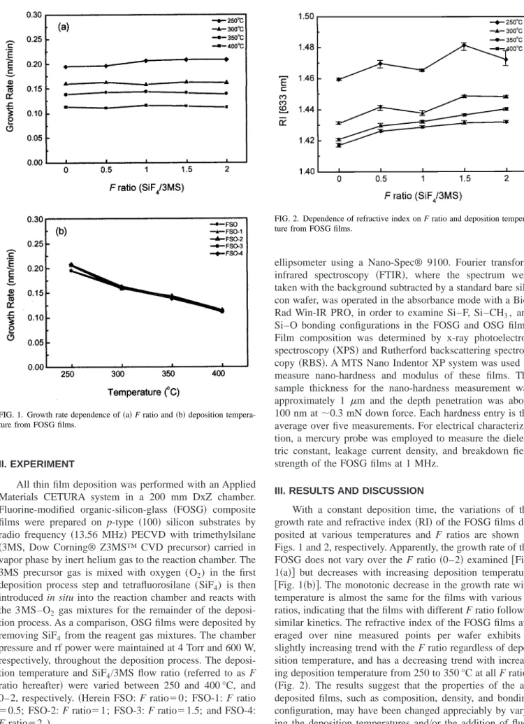
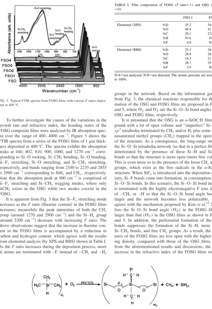
With a constant deposition time, the variations of the growth rate and refractive index 共RI兲 of the FOSG films de- posited at various temperatures and F ratios are shown in Figs. 1 and 2, respectively. Apparently, the growth rate of the FOSG does not vary over the F ratio 共0–2兲 examined 关Fig.
1 共a兲兴 but decreases with increasing deposition temperature 关Fig. 1共b兲兴. The monotonic decrease in the growth rate with temperature is almost the same for the films with various F ratios, indicating that the films with different F ratio follow a similar kinetics. The refractive index of the FOSG films av- eraged over nine measured points per wafer exhibits a slightly increasing trend with the F ratio regardless of depo- sition temperature, and has a decreasing trend with increas- ing deposition temperature from 250 to 350 °C at all F ratios 共Fig. 2兲. The results suggest that the properties of the as- deposited films, such as composition, density, and bonding configuration, may have been changed appreciably by vary- ing the deposition temperatures and/or the addition of fluo- rine. Also, the deposition temperature seems to dominate over the F ratio in affecting film properties.
FIG. 1. Growth rate dependence of
共a兲 F ratio and 共b兲 deposition tempera-
ture from FOSG films.FIG. 2. Dependence of refractive index on F ratio and deposition tempera- ture from FOSG films.
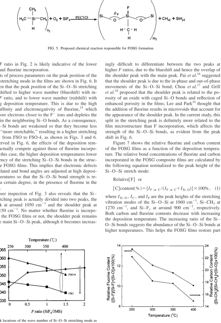
To further investigate the causes of the variations in the growth rate and refractive index, the bonding states of the FOSG composite films were analyzed by IR absorption spec- tra over the range of 400– 4000 cm
⫺1. Figure 3 shows the FTIR spectra from a series of the FOSG films of 1 m thick- ness deposited at 400 °C. The spectra exhibit the absorption peaks at 440, 802, 810, 900, 1060, and 1270 cm
⫺1corre- sponding to Si–O rocking, Si–CH
3bending, Si–O bending, Si–F
xstretching, Si–O stretching, and Si–CH
3stretching, respectively, and bands ranging from 2100 to 2235 and 2855 to 2960 cm
⫺1corresponding to SiH
xand CH
x, respectively.
Note that the absorption peak at 900 cm
⫺1is comprised of Si–F
xstretching and Si–CH
3wagging modes, where only SiCH
3exists in the OSG while two modes coexist in the FOSG.
It is apparent from Fig. 3 that the Si–F
xstretching mode increases as the F ratio 共fluorine content兲 in the FOSG films increases; meanwhile the peak intensities of both the CH
xgroup 共around 1270 and 2900 cm⫺1兲 and the Si–H
x group 共around 2200 cm⫺1兲 decrease with increasing F ratio. The above observations suggest that the increase in fluorine con- tent in the FOSG films is accompanied by a reduction in carbon and hydrogen content, which agrees with the results from elemental analysis 共by XPS and RBS兲 shown in Table I.
兲 decrease with increasing F ratio. The above observations suggest that the increase in fluorine con- tent in the FOSG films is accompanied by a reduction in carbon and hydrogen content, which agrees with the results from elemental analysis 共by XPS and RBS兲 shown in Table I.
As the F ratio increases during the deposition process, more Si atoms are terminated with –F, instead of – CH
xand – H
xgroups in the network. Based on the information gathered from Fig. 3, the chemical reactions responsible for the for- mation of the OSG and FOSG films are proposed in Figs. 4 and 5, where ⍜Cand ⍜Fare the Si–O–Si bond angles in the OSG and FOSG films, respectively.
are the Si–O–Si bond angles in the OSG and FOSG films, respectively.
It is presumed that the OSG is an a-SiOC:H film com- pound with a lot of open volume and ‘‘imperfect’’ Si–O–Si s p
3tetrahedra terminated by CH
3and/or H, plus some loose, unsaturated methyl groups (CH
x) trapped in the open cores of the structure. As a consequence, the long-range order of the Si–O–Si tetradedra network 共as that in a perfect SiO2) is deteriorated by the presence of these Si–H and Si–CH
3
bonds so that the structure is more open 共more free volume兲.
This is even more so in the presence of the loose CH
xmethyl groups, which exist as the free radicals in the a-SiOC:H structure. When SiF
4is introduced into the deposition chem- istry, Si–F bonds come into formation, in consumption of the Si–O–Si bonds. In this scenario, the Si–O–Si bond network is terminated with the highly electronegative F ions instead of – CH
3or –H so that the Si–O–Si bond angle becomes larger and the network becomes less polarizable, which agrees with the mechanism proposed by Kim et al.
15There- fore the Si–O–Si bond angle ( ⍜F) in the FOSG films is larger than that ( ⍜C) in the OSG films as shown in Figs. 4 and 5. In addition, the preferential formation of the Si–F bonds suppresses the formation of the Si–H, more bulky Si–CH
3 bonds, and free CH
x groups. As a result, the struc- tures of the FOSG films are less open with the higher pack- ing density, compared with those of the OSG films. Also, from the aforementioned results and discussions, the slight increase in the refractive index of the FOSG films with in-
) in the OSG films as shown in Figs. 4 and 5. In addition, the preferential formation of the Si–F bonds suppresses the formation of the Si–H, more bulky Si–CH
3bonds, and free CH
xgroups. As a result, the struc- tures of the FOSG films are less open with the higher pack- ing density, compared with those of the OSG films. Also, from the aforementioned results and discussions, the slight increase in the refractive index of the FOSG films with in-
FIG. 3. Typical FTIR spectra from FOSG films with various F ratios depos- ited at 400 °C.
FIG. 4. Proposed chemical reaction responsible for OSG formation.
Elemental
共RBS兲
%Si 25.3 18⫾3
%O 28.8 26
⫾3
%C 14.3 21
⫾3
%H 28.7 35
⫾3
%F 2.9 N/D
N/A
⫽not analyzed, N/D⫽not detected. The atomic percents are normalized
to 100%.creasing F ratio in Fig. 2 is likely indicative of the lower porosity and fluorine incorporation.
Effects of process parameters on the peak position of the Si–O–Si stretching mode in the films are shown in Fig. 6. It can be seen that the peak position of the Si–O–Si stretching mode is shifted to higher wave number 共blueshift兲 with in- creasing F ratio, and to lower wave number 共redshift兲 with decreasing deposition temperature. This is due to the high electron affinity and electronegativity of fluorine,
15which attracts more electrons closer to the F
⫺ions and depletes the electrons in the neighboring Si–O bonds. As a consequence, the Si–O–Si bonds are weakened so that they become less rigid and ‘‘more stretchable,’’ resulting in a higher stretching frequency from FSO to FSO-4, as shown in Figs. 3 and 6.
Also observed in Fig. 6, the effects of the deposition tem- perature actually compete against those of fluorine incorpo- ration. In this case, the higher deposition temperatures lower the frequency of the stretching Si–O–Si bonds in the struc- ture of the FOSG films. This implies that electronic defects are annihilated and bond angles are adjusted at high deposi- tion temperatures so that the Si–O–Si bond strength is re- stored to a certain degree, in the presence of fluorine in the structures.
A closer inspection of Fig. 3 also reveals that the Si–
O–Si stretching peak is actually divided into two peaks, the main peak at around 1050 cm
⫺1and the shoulder peak at around 1150 cm
⫺1. No matter whether fluorine is incorpo- rated into the FOSG films or not, the shoulder peak remains behind the main Si–O–Si peak, although it becomes increas-
ingly difficult to differentiate between the two peaks at higher F ratios, due to the blueshift and hence the overlap of the shoulder peak with the main peak. Pai et al.
16suggested that the shoulder peak is due to the in-phase and out-of-phase movements of the Si–O–Si bond; Chou et al.
17and Grill et al.
18proposed that the shoulder peak is related to the po- rosity of an oxide with caged Si–O bonds and reflection of enhanced porosity in the films; Lee and Park
19thought that the addition of fluorine results in microvoids that account for the appearance of the shoulder peak. In the current study, this split in the stretching peak is definitely more related to the film microstructure than F incorporation, which affects the strength of the Si–O–Si bonds, as evident from the peak shift in Fig. 6.
Figure 7 shows the relative fluorine and carbon content of the FOSG films as a function of the deposition tempera- ture. The relative bond concentrations of fluorine and carbon incorporated in the FOSG composite films are calculated by the following equation normalized to the peak height of the Si–O–Si stretch mode:
Relative 关F兴 or
关C兴content共%兲⫽ 兵 IF or C/ 共I
F or C⫹I
Si–O兲 其 ⫻100%, 共1兲 where ISi–O, I
C, and I
Fare the peak heights of the stretching vibration modes of the Si–O–Si at 1060 cm
⫺1, Si–CH
3 at 1270 cm
⫺1, and Si–F
x at around 900 cm
⫺1, respectively.
Both carbon and fluorine contents decrease with increasing the deposition temperature. The increasing ratio of the Si–
O–Si bonds suggests the abundance of the Si–O–Si bonds at higher temperatures. This helps the FOSG films restore part
FIG. 5. Proposed chemical reaction responsible for FOSG formation.
FIG. 6. Peak locations of the wave number of Si–O–Si stretching mode as a function of F ratio
共deposited at 350 °C typically兲 and deposition tempera-
ture.FIG. 7. Relative fluorine and carbon content incorporated in FSO-4 films as a function of deposition temperature.
of the bond integrity and tetrahedral structure of a perfect SiO
2, leading to the improved mechanical properties as shown below.
Mechanical hardness and modulus of elasticity of the resulting OSG and FOSG films are plotted as a function of F ratio in Fig. 8. The figure clearly exhibits a trend of improve- ment in hardness and modulus as the F ratio increases, which can be attributed to the higher packing density of the films due to the less loose CH
xmethyl groups by fluorine incor- poration, as discussed previously. Meanwhile, it is noted that the hardness 共2 to 3 GPa兲 of the FOSG films at 400 °C is higher than that of the OSG 共⬃1.5 GPa兲 films with more free volume. That makes the FOSG a potential 共and better兲 sub- stitute for the OSG to be implemented as an IMD film in the integration scheme.
Figure 9 shows the permittivity 共dielectric constant兲 of the thin films measured at 1 MHz. Apparently, the dielectric constant decreases slightly as the F ratio increases in general, and the films deposited at the lower temperatures exhibit the lower values. Lim et al.
20proposed that fluorine attracts and replaces relatively more polarizable constituents, which leads subsequently to the lower dielectric constant. Shapiro et al.
21suggest that replacing the Si–O in the SiO
2matrix with the
Si–F reduces the electronic polarizability of the matrix and thus the electronic contribution to the dielectric constant.
From Fig. 9, the lowering of the dielectric constant in the FOSG films with increasing F ratio is due to the polarizabil- ity of the (SiO
3F) tetrahedral structure, which has been de- scribed in Fig. 5, despite the higher packing density in these films. In this case, ionization polarization, instead of elec- tronic polarization, seems to play a dominant role in the re- duction of permittivity in the FOSG, since the refractive in- dex actually increases with F ratio as shown in Fig. 2.
Figure 10 shows the dependence of the leakage current on the electric field from the FOSG 共J-E plot兲 films of vari- ous F ratios and deposition temperatures, relative to that from a typical OSG film. The leakage current increases with the electric field, and two plateaus can be clearly identified in the fluorine-incorporated films. On the other hand, the J-E plot of the FSO 共OSG兲 film does not exhibit a plateau in its:
J-E plot, opposed to all the others in Fig. 10. Supposedly, this is the result of two forms of the bonding configuration existing in the FOSG films. The higher plateau is associated with the fluorine-incorporated structure while the lower one related to the relatively fluorine-free structure. In addition, there is a strong temperature effect on the breakdown field of the FSO-4. This can also be attributed to the changes in the bonding configuration at various temperatures. As shown in Figs. 6 and 7, the lower temperature results in the more stretchable Si–O–Si bonds, more CH
xgroups, and more free volume present in the films. Therefore the breakdown field strength decreases at the lower temperatures. The breakdown field of the investigated FOSG films deposited at high tem- peratures is in the range of 6.5– 8.5 MV/cm, which is higher than that of the fluorine-free OSG film. This result suggests that the modified FOSG films are excellent candidates for the IMD layers in the ultralarge scale integration circuit applica- tions.
IV. CONCLUSION
The composition, bonding configuration, optical, me- chanical, and electrical properties of in situ fluorine-modified OSG 共FOSG兲 films using trimethelysilane 共3MS兲, tetrafluo-
FIG. 8. Mechanical hardness and modulus plotted as a function of F ratio from FOSG films deposited at 400 °C.
FIG. 9. Dielectric constant of FOSG films as a function of F ratio for various deposition temperatures.
FIG. 10. Typical leakage current density and breakdown field strength from FOSG films deposited at various temperatures and F ratios.
rosilane (SiF
4), and oxygen (O
2) as precursors by the PECVD method have been investigated. The refractive index of the FOSG decreases with increasing deposition tempera- ture yet increases with increasing fluorine content in the films. Higher fluorine content in the FOSG films also ac- counted for the improved mechanical hardness and modulus, and the lower dielectric constant. Compared with the OSG films, the FOSG films exhibit a bimodal behavior in the di- electric breakdown and the higher deposition temperatures improve their breakdown field strength. These results can be accounted for by the changes in composition and bonding configuration, as determined from FTIR and elemental analyses. Relatively speaking, the modified FOSG appears to be a more promising low dielectric constant material for IMD application than the OSG.
ACKNOWLEDGMENTS
The authors gratefully acknowledge technical and finan- cial support from Air Products and Chemicals, Inc., and Tai- wan Semiconductor Manufacturing Company Ltd.
1L. Peters, Semicond. Int. 23, 108
共2000兲.
2Z.-C. Wu et al., J. Electrochem. Soc. 148, F115
共2002兲.
3W. Chang, S. M. Jang, C. H. Yu, S. C. Sun, and M. S. Liang, in Proceed- ings of 1999 IEEE IITC
共IEEE, New York, 1999兲, p. 131.
4J. Ida, M. Yoshimaru, T. Usami, A. Ohtomo, K. Shimokawa, A. Kita, and
M. Ino, in Proceedings of 1994 IEEE VLSI
共IEEE, New York, 1994兲, p.
59.
5T. Fukuda, T. Hosokawa, Y. Nakamura, K. Katoh, and N. Kobayashi, in Proceedings of 1996 IEEE VLSI
共IEEE, New York, 1996兲, p. 114.
6S. W. Lim, Y. Shimogaki, Y. Nakano, and K. Tada, Appl. Phys. Lett. 68, 832
共1996兲.
7S. M. Han and E. Aydil, J. Vac. Sci. Technol. A 15, 2893
共1997兲.
8M. J. Shapiro, S. V. Nguyen, T. Matsuda, and D. Dobuzinsky, Thin Solid Films 270, 503
共1995兲.
9W. S. Yoo, R. Swope, B. Sparks, and D. Mordo, J. Mater. Res. 12, 70
共1997兲.
10S. M. Han and E. S. Aydil, J. Appl. Phys. 83, 2172
共1998兲.
11C. Kittel, Introduction to Solid State Physics, 7th ed.
共Wiley, New York,
1996兲, Chap. 13.
12H. Miyajima, R. Katsumata, Y. Nakasaki, and N. Hayasaka, Jpn. J. Appl.
Phys., Part 1 35, 6217
共1996兲.
13G. Y. Lee, D. C. Edelstein, R. Conti, W. Cote, K.-S. Low, D. Dobuzinsky, G. Feng, K. Dev, P. Wrschka, P. Shafer, R. Ramachandran, A. Simpson, E.
Liniger, E. Simonyi, T. Dalton, T. Spooner, C. Jahnes, E. Kaltalioglu, and A. Grill, Advanced Metallization Conference, San Diego, CA, 2000.
14A. Grill and V. Patel, Mater. Res. Soc. Symp. Proc. 612, D2.9.1
共2000兲.
15Y.-H. Kim, M. S. Hwang, and H. J. Kim, J. Appl. Phys. 90, 3367
共2001兲.
16P. G. Pai, S. S. Chao, Y. Takagi, and G. Lucovsky, J. Vac. Sci. Technol. A 4, 689
共1986兲.
17J.-S. Chou and S.-C. Lee, J. Appl. Phys. 77, 1805
共1995兲.
18A. Grill and V. Patel, Appl. Phys. Lett. 79, 803
共2001兲.
19S. Lee and J.-W. Park, J. Appl. Phys. 80, 5260
共1996兲.
20S. W. Lim, Y. Shimogaki, Y. Nakano, and K. Tada, J. Electrochem. Soc.
144, 2531
共1997兲.
21M. J. Shapiro, S. V. Nguyen, T. Matsuda, and D. Dobuzinsky, Thin Solid Films 270, 503